 | –≠–ª–µ–∫—Ç—Ä–æ–Ω–Ω—ã–π –∫–æ–º–ø–æ–Ω–µ–Ω—Ç: LTC1967 | –°–∫–∞—á–∞—Ç—å:  PDF PDF  ZIP ZIP |
1
LTC1967
1967f
Precision Extended
Bandwidth, RMS-to-DC Converter
s
High Linearity:
0.02% Linearity Allows Simple System Calibration
s
Wide Input Bandwidth:
Bandwidth to 0.1% Additional Gain Error: 40kHz
Bandwidth Independent of Input Voltage Amplitude
s
No-Hassle Simplicity:
True RMS-DC Conversion with Only One External
Capacitor
Delta Sigma Conversion Technology
s
Low Supply Current:
330
µ
A Typ
s
Ultralow Shutdown Current:
0.1
µ
A
s
Flexible Inputs:
Differential or Single Ended
Rail-to-Rail Common Mode Voltage Range
Up to 1V
PEAK
Differential Voltage
s
Flexible Output:
Rail-to-Rail Output
Separate Output Reference Pin Allows Level Shifting
s
Small Size:
Space Saving 8-Pin MSOP Package
s
True RMS Digital Multimeters and Panel Meters
s
True RMS AC + DC Measurements
DESCRIPTIO
U
FEATURES
APPLICATIO S
U
The LTC
Æ
1967 is a true RMS-to-DC converter that uses an
innovative delta-sigma computational technique. The ben-
efits of the LTC1967 proprietary architecture when com-
pared to conventional log-antilog RMS-to-DC converters
are higher linearity and accuracy, bandwidth independent
of amplitude and improved temperature behavior.
The LTC1967 operates with single-ended or differential in-
put signals (for EMI/RFI rejection) and supports crest fac-
tors up to 4. Common mode input range is rail-to-rail. Dif-
ferential input range is 1V
PEAK
, and offers unprecedented
linearity. The LTC1967 allows hassle-free system calibra-
tion at any input voltage.
The LTC1967 has a rail-to-rail output with a separate out-
put reference pin providing flexible level shifting; it oper-
ates on a single power supply from 4.5V to 5.5V. A low power
shutdown mode reduces supply current to 0.1
µ
A.
The LTC1967 is packaged in the space-saving MSOP pack-
age, which is ideal for portable applications.
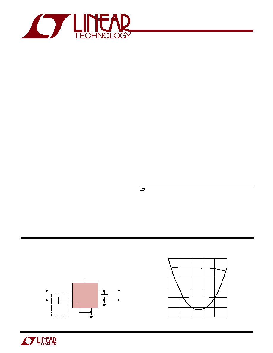
Single Supply RMS-to-DC Converter
C
AVE
1
µ
F
V
OUT
+
≠
1967 TA01
4.5V TO 5.5V
OUTPUT
DIFFERENTIAL
INPUT
LTC1967
V
+
0.1
µ
F
OPT. AC
COUPLING
EN
GND
OUT RTN
IN1
IN2
TYPICAL APPLICATIO
U
V
IN
(mV AC
RMS
)
0
≠1.0
LINEARITY ERROR (V
OUT
mV DC ≠ V
IN
mV AC
RMS
)
≠0.8
≠0.6
≠0.4
≠0.2
0
0.2
100
200
300
400
1967 TA01b
500
LTC1967,
60Hz SINEWAVE
CONVENTIONAL
LOG/ANTILOG
Linearity Performance
, LTC and LT are registered trademarks of Linear Technology Corporation.
Protected under U.S. Patent Numbers 6,359,576, 6,362,677 and 6,516,291

2
LTC1967
1967f
Supply Voltage
V
+
to GND ............................................................. 6V
Input Currents (Note 2) .....................................
±
10mA
Output Current (Note 3) .....................................
±
10mA
ENABLE Voltage ......................................... ≠0.3V to 6V
OUT RTN Voltage ........................................ ≠0.3V to V
+
Operating Temperature Range (Note 4)
LTC1967C/LTC1967I ......................... ≠ 40
∞
C to 85
∞
C
Specified Temperature Range (Note 5)
LTC1967C/LTC1967I ......................... ≠ 40
∞
C to 85
∞
C
Maximum Junction Temperature ......................... 150
∞
C
Storage Temperature Range ................ ≠ 65
∞
C to 150
∞
C
Lead Temperature (Soldering, 10 sec)................. 300
∞
C
ORDER PART
NUMBER
LTC1967CMS8
LTC1967IMS8
T
JMAX
= 150
∞
C,
JA
= 220
∞
C/ W
ABSOLUTE AXI U RATI GS
W
W
W
U
PACKAGE/ORDER I FOR ATIO
U
U
W
(Note 1)
MS8 PART MARKING
LTTJ
The
q
denotes specifications which apply over the full operating
temperature range, otherwise specifications are T
A
= 25
∞
C. V
+
= 5V, V
OUTRTN
= 2.5V, C
AVE
= 10
µ
F, V
IN
= 200mV
RMS
, V
ENABLE
= 0.5V
unless otherwise noted.
ELECTRICAL CHARACTERISTICS
Consult LTC Marketing for parts specified with wider operating temperature ranges.
1
2
3
4
GND
IN1
IN2
NC
8
7
6
5
ENABLE
V
+
OUT RTN
V
OUT
TOP VIEW
MS8 PACKAGE
8-LEAD PLASTIC MSOP
SYMBOL
PARAMETER
CONDITIONS
MIN
TYP
MAX
UNITS
Conversion Accuracy
G
ERR
Low Frequency Gain Error
50Hz to 5kHz Input (Notes 6, 7)
±
0.1
±
0.3
%
q
±
0.4
%
V
OOS
Output Offset Voltage
(Notes 6, 7)
0.1
0.55
mV
V
OOS
/
T
Output Offset Drift
(Note 11)
q
2
10
µ
V/
∞
C
LIN
ERR
Linearity Error
50mV to 350mV (Notes 7, 8)
q
0.02
0.15
%
PSRRG
Power Supply Rejection
(Note 9)
0.02
0.15
%/V
q
0.20
%/V
V
IOS
Input Offset Voltage
(Notes 6, 7, 10)
0.2
1.5
mV
V
IOS
/
T
Input Offset Drift
(Note 11)
q
1
10
µ
V/
∞
C
Additional Error vs Crest Factor (CF)
CF = 3
60Hz Fundamental, 200mV
RMS
q
0.2
mV
CF = 5
60Hz Fundamental, 200mV
RMS
q
5
mV
Input Characteristics
V
IMAX
Maximum Peak Input Swing
Accuracy = 1% (Note 14)
q
1
1.05
V
I
VR
Input Voltage Range
q
0
V
+
V
Z
IN
Input Impedance
Average, Differential (Note 12)
5
M
Average, Common Mode (Note 12)
100
M
CMRRI
Input Common Mode Rejection
(Note 13)
q
50
400
µ
V/V
V
IMIN
Minimum RMS Input
q
5
mV
PSRRI
Power Supply Rejection
(Note 9)
q
250
600
µ
V/V
3
LTC1967
1967f
The
q
denotes specifications which apply over the full operating
temperature range, otherwise specifications are T
A
= 25
∞
C. V
+
= 5V, V
OUTRTN
= 2.5V, C
AVE
= 10
µ
F, V
IN
= 200mV
RMS
, V
ENABLE
= 0.5V
unless otherwise noted.
ELECTRICAL CHARACTERISTICS
Note 1: Absolute Maximum Ratings are those values beyond which the life
of a device may be impaired.
Note 2: The inputs (IN1, IN2) are protected by shunt diodes to GND and
V
+
. If the inputs are driven beyond the rails, the current should be limited
to less than 10mA.
Note 3: The LTC1967 output (V
OUT
) is high impedance and can be
overdriven, either sinking or sourcing current, to the limits stated.
Note 4: The LTC1967C/LTC1967I are guaranteed functional over the
operating temperature range of ≠ 40
∞
C to 85
∞
C.
Note 5: The LTC1967C is guaranteed to meet specified performance from
0
∞
C to 70
∞
C. The LTC1967C is designed, characterized and expected to
meet specified performance from ≠ 40
∞
C to 85
∞
C but is not tested nor QA
sampled at these temperatures. The LTC1967I is guaranteed to meet
specified performance from ≠ 40
∞
C to 85
∞
C.
Note 6: High speed automatic testing cannot be performed with
C
AVE
= 10
µ
F. The LTC1967 is 100% tested with C
AVE
= 47nF. Correlation
tests have shown that the performance limits can be guaranteed with the
additional testing being performed to guarantee proper operation of all the
internal circuitry.
Note 7: High speed automatic testing cannot be performed with 60Hz
inputs. The LTC1967 is 100% tested with DC and 10kHz input signals.
Measurements with DC inputs from 50mV to 350mV are used to calculate
the four parameters: G
ERR
, V
OOS
, V
IOS
and linearity error. Correlation tests
have shown that the performance limits can be guaranteed with the
additional testing being performed to guarantee proper operation of all
internal circuitry.
Note 8: The LTC1967 is inherently very linear. Unlike older log/antilog
circuits, its behavior is the same with DC and AC inputs, and DC inputs are
used for high speed testing.
Note 9: The power supply rejections of the LTC1967 are measured with
DC inputs from 50mV to 350mV. The change in accuracy from V
+
= 4.5V
to V
+
= 5.5V is divided by 1V.
Note 10: Previous generation RMS-to-DC converters required nonlinear
input stages as well as a nonlinear core. Some parts specify a "DC reversal
error," combining the effects of input nonlinearity and input offset voltage.
The LTC1967 behavior is simpler to characterize and the input offset
voltage is the only significant source of "DC reversal error."
Note 11: Guaranteed by design.
Note 12: The LTC1967 is a switched capacitor device and the input/output
impedance is an average impedance over many clock cycles. The input
impedance will not necessarily lead to an attenuation of the input signal
measured. Refer to the Applications Information section titled "Input
Impedance" for more information.
SYMBOL
PARAMETER
CONDITIONS
MIN
TYP
MAX
UNITS
Output Characteristics
OVR
Output Voltage Range
q
0
V
+
V
Z
OUT
Output Impedance
(Note 12)
q
40
50
65
k
CMRRO
Output Common Mode Rejection
(Note 13)
q
50
250
µ
V/V
V
OMAX
Maximum Differential Output Swing
Accuracy = 1%, DC Input (Note 14)
1.0
1.05
V
q
0.9
V
PSRRO
Power Supply Rejection
(Note 9)
q
250
1000
µ
V/V
Frequency Response
f
1P
0.1% Additional Gain Error (Note 15)
40
kHz
f
≠ 3dB
±
3dB Frequency (Note 15)
4
MHz
Power Supplies
V
+
Supply Voltage
q
4.5
5.5
V
I
S
Supply Current
IN1 = 20mV, IN2 = 0V
q
320
390
µ
A
IN1 = 200mV, IN2 = 0V
340
µ
A
Shutdown Characteristics
I
SS
Supply Current
V
ENABLE
= 4.5V
q
0.1
10
µ
A
I
IH
ENABLE Pin Current High
V
ENABLE
= 4.5V
q
≠ 1
≠ 0.1
µ
A
I
IL
ENABLE Pin Current Low
V
ENABLE
= 0.5V
q
≠3
≠0.5
≠ 0.1
µ
A
V
TH
ENABLE Threshold Voltage
2.1
V
V
HYS
ENABLE Threshold Hysteresis
0.1
V

4
LTC1967
1967f
ELECTRICAL CHARACTERISTICS
Note 13: The common mode rejection ratios of the LTC1967 are measured
with DC inputs from 50mV to 350mV. The input CMRR is defined as the
change in V
IOS
measured between input levels of 0V to 350mV and input
levels of V
+
≠ 350mV to V
+
divided by V
+
≠ 350mV. The output CMRR is
defined as the change in V
OOS
measured with OUT RTN = 0V and OUT RTN
= V
+
≠ 350mV divided by V
+
≠ 350mV.
Note 14: The LTC1967 input and output voltage swings are limited by
internal clipping. However, its
topology is relatively tolerant of
momentary internal clipping.
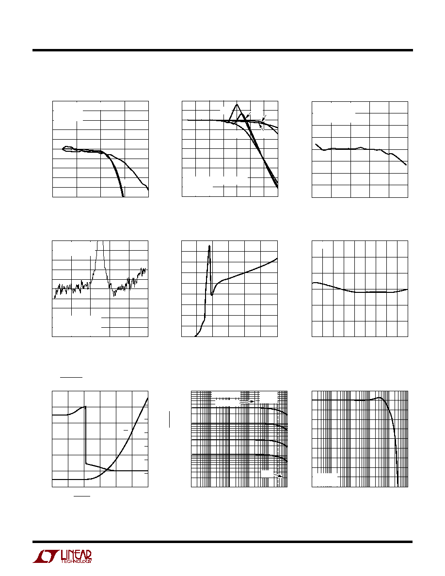
TYPICAL PERFOR A CE CHARACTERISTICS
U
W
Gain and Offset
vs Output Common Mode Voltage
Gain and Offset
vs Input Common Mode Voltage
Note 15: The LTC1967 exploits oversampling and noise shaping to reduce
the quantization noise of internal 1-bit analog-to-digital conversions. At
higher input frequencies, increasingly large portions of this noise are
aliased down to DC. Because the noise is shifted in frequency, it becomes
a low frequency rumble and is only filtered at the expense of increasingly
long settling times. The LTC1967 is inherently wideband, but the output
accuracy is degraded by this aliased noise.
INPUT COMMON MODE VOLTAGE (V)
0
≠0.7
GAIN ERROR (%)
OFFSET VOLTAGE (mV)
≠0.6
≠0.4
≠0.3
≠0.2
0.3
0
1.0
2.0 2.5
5.0
4.5
1967 G01
≠0.5
0.1
0.2
≠0.1
≠1.0
≠0.8
≠0.4
≠0.2
0
1.0
0.4
≠0.6
0.6
0.8
0.2
0.5
50mV
V
IN(PEAK)
350mV
1.5
3.0 3.5 4.0
V
IOS
V
OOS
GAIN ERROR
OUTPUT COMMON MODE VOLTAGE (V)
0
≠0.5
GAIN ERROR (%)
OFFSET VOLTAGE (mV)
≠0.4
≠0.2
≠0.1
0
0.5
0.2
1.0
2.0 2.5
5.0
4.5
1967 G02
≠0.3
0.3
0.4
0.1
≠1.0
≠0.8
≠0.4
≠0.2
0
1.0
0.4
≠0.6
0.6
0.8
0.2
0.5
1.5
3.0 3.5 4.0
V
IOS
V
OOS
GAIN ERROR
50mV
V
IN(PEAK)
350mV
Gain and Offsets vs Temperature
Gain and Offset vs Supply Voltage
TEMPERATURE (
∞
C)
≠40
GAIN ERROR (%)
OFFSET VOLTAGE (mV)
0.01
0.03
0.05
V
OOS
60
1967 G03
≠0.01
≠0.03
0
0.02
0.04
≠0.02
≠0.04
≠0.05
0.1
0
0.3
0.5
≠0.1
≠0.3
0.2
0.4
≠0.2
≠0.4
≠0.5
≠15
10
35
85
V
IOS
GAIN ERROR
50mV
V
IN(PEAK)
350mV
SUPPLY VOLTAGE (V)
4.5
≠0.5
GAIN ERROR (%)
OFFSET VOLTAGE (mV)
≠0.4
≠0.2
≠0.1
0
0.5
0.2
4.8
5.1
6.0
1967 G04
≠0.3
0.3
0.4
0.1
≠1.0
≠0.8
≠0.4
≠0.2
0
1.0
0.4
≠0.6
0.6
0.8
0.2
5.4
5.7
V
IOS
V
OOS
GAIN ERROR
50mV
V
IN(PEAK)
350mV
5
LTC1967
1967f
TYPICAL PERFOR A CE CHARACTERISTICS
U
W
Performance vs Large Crest Factors
AC Linearity
DC Linearity
Supply Current vs Supply Voltage
Supply Current vs Temperature
Shutdown Current
vs ENABLE Voltage
Input Signal Bandwidth
vs RMS Value
Performance vs Crest Factor
CREST FACTOR
1
199.0
199.8
199.6
199.4
199.2
OUTPUT VOLTAGE (mV DC)
200.0
200.2
200.4
200.6
2
3
4
5
1kHz
1967 G05
200.8
201.0
200mV
RMS
SCR WAVEFORMS
C
AVE
= 10
µ
F
O.1%/DIV
60Hz
20Hz
CREST FACTOR
1
OUTPUT VOLTAGE (mV DC)
220
4
1967 G06
190
170
2
3
5
160
150
140
130
120
210
200
180
6
7
8
200mV
RMS
SCR WAVEFORMS
C
AVE
= 10
µ
F
5%/DIV
60Hz
10Hz
10kHz
1kHz
20Hz
V
IN1
(mV AC
RMS
)
0
V
OUT
(mV DC) ≠ V
IN
(mV AC
RMS
)
0.20
0.15
0.10
0.05
0
≠0.05
≠0.10
≠0.15
≠0.20
400
1967 G07
100
200
300
500
60Hz SINEWAVES
C
AVE
= 10
µ
F
V
IN2
= MIDSUPPLY
V
IN1
(mV)
≠500
{V
OUTDC
≠ |V
INDC
|} (mV)
0.02
0.06
0.10
300
1967 G08
≠0.02
≠0.06
0
0.04
0.08
≠0.04
≠0.08
≠0.10
≠300
≠100
100
500
C
AVE
= 1
µ
F
V
IN2
= MIDSUPPLY
EFFECTS OF OFFSETS
MAY BE POSITIVE OR
NEGATIVE AT V
IN
= 0V
SUPPLY VOLTAGE (V)
0
SUPPLY CURRENT (
µ
A)
4
450
400
350
300
250
200
150
100
50
0
1967 G09
2
6
3
1
5
TEMPERATURE (
∞
C)
≠55
315
SUPPLY CURRENT (
µ
A)
320
330
335
340
≠15
25
45
125
1967 G10
325
≠35
5
65
85 105
345
V
S
= 5V
ENABLE PIN VOLTAGE (V)
0
500
400
300
200
100
0
≠100
0
≠100
100
I
S
I
EN
≠200
200
≠300
300
≠400
3
5
1967 G11
1
2
4
6
SUPPLY CURRENT (
µ
A)
ENABLE PIN CURRENT (nA)
INPUT SIGNAL FREQUENCY (Hz)
10
OUTPUT DC VOLTAGE (mV)
100
100
10k
100k
1M
1967 G12
1
1k
1000
10M
0.1% ERROR
10%
ERROR
≠3dB
1% ERROR
Input Signal Bandwidth
INPUT SIGNAL FREQUENCY (Hz)
100
190
OUTPUT DC VOLTAGE (mV)
192
194
196
198
1k
10k
100k
1M
10M
1967 G13
188
186
184
182
200
202
1%/DIV
C
AVE
= 1
µ
F