 | –≠–ª–µ–∫—Ç—Ä–æ–Ω–Ω—ã–π –∫–æ–º–ø–æ–Ω–µ–Ω—Ç: LTC1968 | –°–∫–∞—á–∞—Ç—å:  PDF PDF  ZIP ZIP |
1
LTC1968
1968f
Precision Wide Bandwidth,
RMS-to-DC Converter
High Linearity:
0.02% Linearity Allows Simple System Calibration
Wide Input Bandwidth:
Bandwidth to 1% Additional Gain Error: 500kHz
Bandwidth to 0.1% Additional Gain Error: 150kHz
3dB Bandwidth Independent of Input Voltage
Amplitude
No-Hassle Simplicity:
True RMS-DC Conversion with Only One External
Capacitor
Delta Sigma Conversion Technology
Ultralow Shutdown Current:
0.1µA
Flexible Inputs:
Differential or Single Ended
Rail-to-Rail Common Mode Voltage Range
Up to 1V
PEAK
Differential Voltage
Flexible Output:
Rail-to-Rail Output
Separate Output Reference Pin Allows Level Shifting
Small Size:
Space Saving 8-Pin MSOP Package
True RMS Digital Multimeters and Panel Meters
True RMS AC + DC Measurements
DESCRIPTIO
U
FEATURES
APPLICATIO S
U
The LTC
Æ
1968 is a true RMS-to-DC converter that uses an
innovative delta-sigma computational technique. The ben-
efits of the LTC1968 proprietary architecture, when com-
pared to conventional log-antilog RMS-to-DC converters,
are higher linearity and accuracy, bandwidth independent
of amplitude and improved temperature behavior.
The LTC1968 operates with single-ended or differential in-
put signals and accurately supports crest factors up to 4.
Common mode input range is rail-to-rail. Differential in-
put range is 1V
PEAK
, and offers unprecedented linearity. The
LTC1968 allows hassle-free system calibration at any in-
put voltage.
The LTC1968 has a rail-to-rail output with a separate out-
put reference pin providing flexible level shifting; it oper-
ates on a single power supply from 4.5V to 5.5V. A low power
shutdown mode reduces supply current to 0.1µA.
The LTC1968 is packaged in the space-saving MSOP pack-
age, which is ideal for portable applications.
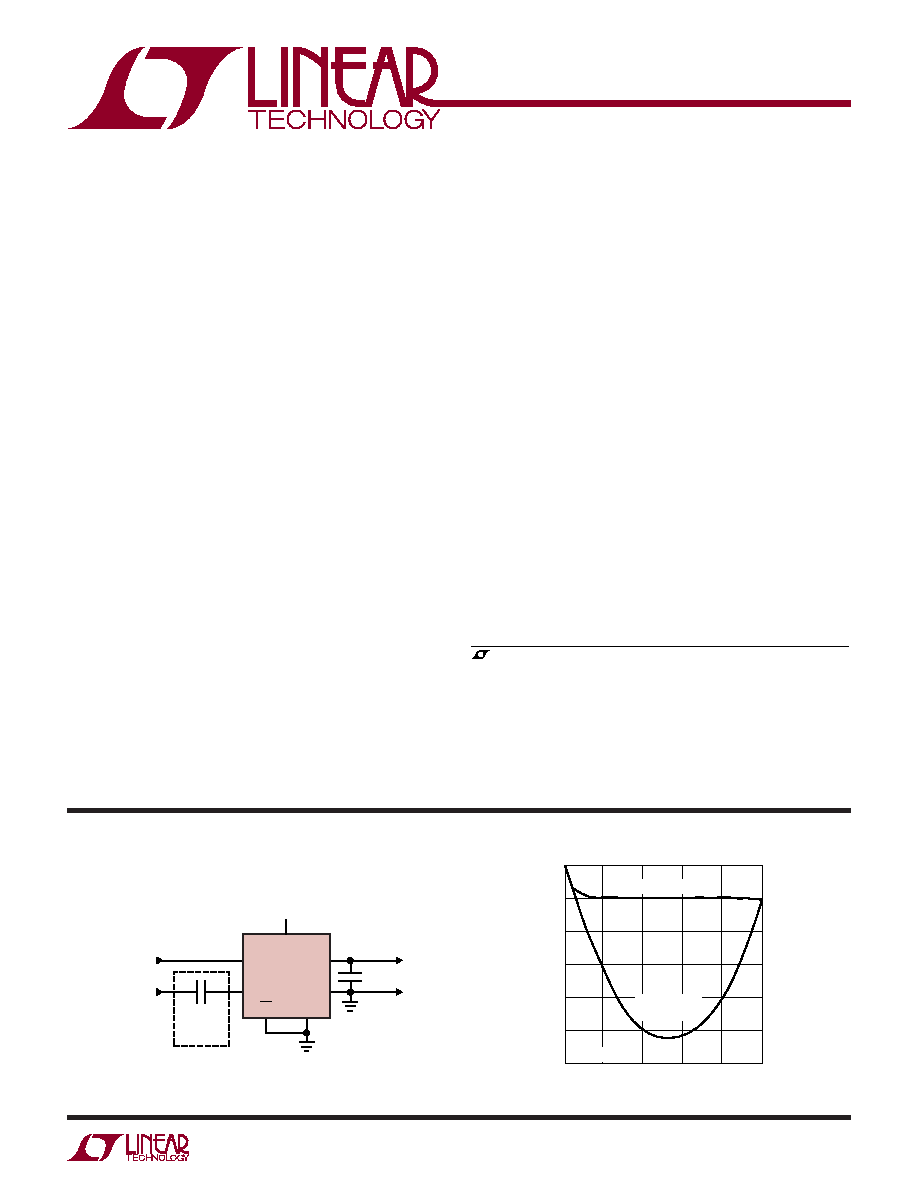
Single Supply RMS-to-DC Converter
C
AVE
10µF
V
OUT
+
≠
1968 TA01
4.5V TO 5.5V
OUTPUT
DIFFERENTIAL
INPUT
LTC1968
V
+
0.1µF
OPT. AC
COUPLING
EN
GND
OUT RTN
IN1
IN2
TYPICAL APPLICATIO
U
V
IN
(mV AC
RMS
)
0
≠1.0
LINEARITY ERROR (V
OUT
mV DC ≠ V
IN
mV AC
RMS
)
≠0.8
≠0.6
≠0.4
≠0.2
0
0.2
100
200
300
400
1968 TA01b
500
LTC1968,
60Hz SINEWAVE
CONVENTIONAL
LOG/ANTILOG
Linearity Performance
, LTC and LT are registered trademarks of Linear Technology Corporation.
Protected under U.S. Patent Numbers 6,359,576, 6,362,677 and 6,516,291
2
LTC1968
1968f
Supply Voltage
V
+
to GND ............................................................. 6V
Input Currents (Note 2) ..................................... ±10mA
Output Current (Note 3) ..................................... ±10mA
ENABLE Voltage ......................................... ≠0.3V to 6V
OUT RTN Voltage ........................................ ≠0.3V to V
+
Operating Temperature Range (Note 4)
LTC1968C/LTC1968I ......................... ≠ 40∞C to 85∞C
Specified Temperature Range (Note 5)
LTC1968C/LTC1968I ......................... ≠ 40∞C to 85∞C
Maximum Junction Temperature ......................... 150∞C
Storage Temperature Range ................ ≠ 65∞C to 150∞C
Lead Temperature (Soldering, 10 sec)................. 300∞C
ORDER PART
NUMBER
LTC1968CMS8
LTC1968IMS8
T
JMAX
= 150∞C,
JA
= 220∞C/ W
ABSOLUTE AXI U RATI GS
W
W
W
U
PACKAGE/ORDER I FOR ATIO
U
U
W
(Note 1)
MS8 PART MARKING
LTAFG
The
denotes specifications which apply over the full operating
temperature range, otherwise specifications are T
A
= 25∞C. V
+
= 5V, V
OUTRTN
= 2.5V, C
AVE
= 10µF, V
IN
= 200mV
RMS
, V
ENABLE
= 0.5V
unless otherwise noted.
ELECTRICAL CHARACTERISTICS
Consult LTC Marketing for parts specified with wider operating temperature ranges.
The temperature grade (I or C) is indicated on the shipping container.
1
2
3
4
GND
IN1
IN2
NC
8
7
6
5
ENABLE
V
+
OUT RTN
V
OUT
TOP VIEW
MS8 PACKAGE
8-LEAD PLASTIC MSOP
SYMBOL
PARAMETER
CONDITIONS
MIN
TYP
MAX
UNITS
Conversion Accuracy
G
ERR
Low Frequency Gain Error
50Hz to 20kHz Input (Notes 6, 7)
±0.1
±0.3
%
±0.4
%
V
OOS
Output Offset Voltage
(Notes 6, 7)
0.2
0.75
mV
V
OOS
/T
Output Offset Voltage Drift
(Note 11)
2
10
µV/∞C
LIN
ERR
Linearity Error
50mV to 350mV (Notes 7, 8)
±0.02
±0.15
%
PSRRG
Power Supply Rejection
(Note 9)
±0.02
±0.20
%/V
±0.25
%/V
V
IOS
Input Offset Voltage
(Notes 6, 7, 10)
0.4
1.5
mV
V
IOS
/T
Input Offset Voltage Drift
(Note 11)
2
10
µV/∞C
Additional Error vs Crest Factor (CF)
CF = 3
60Hz Fundamental, 200mV
RMS
0.2
mV
CF = 5
60Hz Fundamental, 200mV
RMS
5
mV
Input Characteristics
V
IMAX
Maximum Peak Input Swing
Accuracy = 1% (Note 14)
1
1.05
V
I
VR
Input Voltage Range
0
V
+
V
Z
IN
Input Impedance
Average, Differential (Note 12)
1.2
M
Average, Common Mode (Note 12)
100
M
CMRRI
Input Common Mode Rejection
(Note 13)
50
400
µV/V
V
IMIN
Minimum RMS Input
5
mV
PSRRI
Power Supply Rejection
(Note 9)
250
700
µV/V

3
LTC1968
1968f
The
denotes specifications which apply over the full operating
temperature range, otherwise specifications are T
A
= 25∞C. V
+
= 5V, V
OUTRTN
= 2.5V, C
AVE
= 10µF, V
IN
= 200mV
RMS
, V
ENABLE
= 0.5V
unless otherwise noted.
ELECTRICAL CHARACTERISTICS
Note 1: Absolute Maximum Ratings are those values beyond which the life
of a device may be impaired.
Note 2: The inputs (IN1, IN2) are protected by shunt diodes to GND and
V
+
. If the inputs are driven beyond the rails, the current should be limited
to less than 10mA.
Note 3: The LTC1968 output (V
OUT
) is high impedance and can be
overdriven, either sinking or sourcing current, to the limits stated.
Note 4: The LTC1968C/LTC1968I are guaranteed functional over the
operating temperature range of ≠ 40∞C to 85∞C.
Note 5: The LTC1968C is guaranteed to meet specified performance from
0∞C to 70∞C. The LTC1968C is designed, characterized and expected to
meet specified performance from ≠ 40∞C to 85∞C but is not tested nor QA
sampled at these temperatures. The LTC1968I is guaranteed to meet
specified performance from ≠ 40∞C to 85∞C.
Note 6: High speed automatic testing cannot be performed with
C
AVE
= 10µF. The LTC1968 is 100% tested with C
AVE
= 47nF.
Note 7: The LTC1968 is 100% tested with DC and 10kHz input signals.
Measurements with DC inputs from 50mV to 350mV are used to calculate
the four parameters: G
ERR
, V
OOS
, V
IOS
and linearity error. Correlation tests
have shown that the performance limits can be guaranteed with the
additional testing being performed to guarantee proper operation of all
internal circuitry.
Note 8: The LTC1968 is inherently very linear. Unlike older log/antilog
circuits, its behavior is the same with DC and AC inputs, and DC inputs are
used for high speed testing.
Note 9: The power supply rejections of the LTC1968 are measured with
DC inputs from 50mV to 350mV. The change in accuracy from V
+
= 4.5V
to V
+
= 5.5V is divided by 1V.
Note 10: Previous generation RMS-to-DC converters required nonlinear
input stages as well as a nonlinear core. Some parts specify a "DC reversal
error," combining the effects of input nonlinearity and input offset voltage.
The LTC1968 behavior is simpler to characterize and the input offset
voltage is the only significant source of "DC reversal error."
Note 11: Guaranteed by design.
Note 12: The LTC1968 is a switched capacitor device and the input/output
impedance is an average impedance over many clock cycles. The input
impedance will not necessarily lead to an attenuation of the input signal
measured. Refer to the Applications Information section titled "Input
Impedance" for more information.
Note 13: The common mode rejection ratios of the LTC1968 are measured
with DC inputs from 50mV to 350mV. The input CMRR is defined as the
change in V
IOS
measured with the input common mode voltage at 0V and
V
+
, divided by V
+
. The output CMRR is defined as the change in V
OOS
measured with OUT RTN = 0V and OUT RTN = V
+
≠ 350mV divided by
V
+
≠ 350mV.
Note 14: The LTC1968 input and output voltage swings are limited by
internal clipping. However, its topology is relatively tolerant of
momentary internal clipping.
Note 15: The LTC1968 exploits oversampling and noise shaping to reduce
the quantization noise of internal 1-bit analog-to-digital conversions. At
higher input frequencies, increasingly large portions of this noise are
aliased down to DC. Because the noise is shifted in frequency, it becomes
a low frequency rumble and is only filtered at the expense of increasingly
long settling times. The LTC1968 is inherently wideband, but the output
accuracy is degraded by this aliased noise.
SYMBOL
PARAMETER
CONDITIONS
MIN
TYP
MAX
UNITS
Output Characteristics
OVR
Output Voltage Range
0
V
+
V
Z
OUT
Output Impedance
(Note 12)
10
12.5
16
k
CMRRO
Output Common Mode Rejection
(Note 13)
50
250
µV/V
V
OMAX
Maximum Differential Output Swing
Accuracy = 1%, DC Input (Note 14)
1.0
1.05
V
0.9
V
PSRRO
Power Supply Rejection
(Note 9)
250
1000
µV/V
Frequency Response
f
1P
1% Additional Gain Error (Note 15)
500
kHz
f
≠ 3dB
±3dB Frequency (Note 15)
15
MHz
Power Supplies
V
+
Supply Voltage
4.5
5.5
V
I
S
Supply Current
IN1 = 20mV, IN2 = 0V
2.3
2.7
mA
IN1 = 200mV, IN2 = 0V
2.4
mA
Shutdown Characteristics
I
SS
Supply Current
V
ENABLE
= 4.5V
0.1
10
µA
I
IH
ENABLE Pin Current High
V
ENABLE
= 4.5V
≠ 1
≠ 0.1
µA
I
IL
ENABLE Pin Current Low
V
ENABLE
= 0.5V
≠3
≠0.5
≠ 0.1
µA
V
TH
ENABLE Threshold Voltage
2.1
V
V
HYS
ENABLE Threshold Hysteresis
0.1
V

4
LTC1968
1968f
TYPICAL PERFOR A CE CHARACTERISTICS
U
W
Gain and Offset
vs Output Common Mode Voltage
Gain and Offset
vs Input Common Mode Voltage
INPUT COMMON MODE VOLTAGE (V)
0
≠0.5
GAIN ERROR (%)
OFFSET VOLTAGE (mV)
≠0.4
≠0.2
≠0.1
0
0.5
0.2
1.0
2.0 2.5
5.0
4.5
1968 G01
≠0.3
0.3
0.4
0.1
≠1.0
≠0.8
≠0.4
≠0.2
0
1.0
0.4
≠0.6
0.6
0.8
0.2
0.5
1.5
3.0 3.5 4.0
V
IOS
V
OOS
GAIN ERROR
50mV V
IN
350mV
OUTPUT COMMON MODE VOLTAGE (V)
0
≠0.5
GAIN ERROR (%)
OFFSET VOLTAGE (mV)
≠0.4
≠0.2
≠0.1
0
0.5
0.2
1.0
2.0 2.5
5.0
4.5
1968 G02
≠0.3
0.3
0.4
0.1
≠1.0
≠0.8
≠0.4
≠0.2
0
1.0
0.4
≠0.6
0.6
0.8
0.2
0.5
1.5
3.0 3.5 4.0
V
IOS
V
OOS
GAIN ERROR
50mV V
IN
350mV
Gain and Offset vs Temperature
Gain and Offset vs Supply Voltage
SUPPLY VOLTAGE (V)
4.5
GAIN ERROR (%)
OFFSET VOLTAGE (mV)
0.1
0.3
0.5
5.7
1968 G03
≠0.1
≠0.3
0
0.2
0.4
≠0.2
≠0.4
≠0.5
0.2
0
0.6
1.0
≠0.2
≠0.6
0.4
0.8
≠0.4
≠0.8
≠1.0
4.8
5.1
5.4
6.0
V
OOS
V
IOS
GAIN ERROR
50mV V
IN
350mV
TEMPERATURE (∞C)
≠40
≠0.5
GAIN ERROR (%)
OFFSET VOLTAGE (mV)
≠0.4
≠0.2
≠0.1
0
0.5
0.2
≠15
10
85
1968 G04
≠0.3
0.3
0.4
0.1
≠0.5
≠0.4
≠0.2
≠0.1
0
0.5
0.2
≠0.3
0.3
0.4
0.1
35
60
V
IOS
V
OOS
GAIN ERROR
50mV V
IN
350mV

5
LTC1968
1968f
TYPICAL PERFOR A CE CHARACTERISTICS
U
W
Performance vs Large Crest Factor
AC Linearity
DC Linearity
Supply Current vs Supply Voltage
Supply Current vs Temperature
Power Supply and ENABLE Pin
Current vs ENABLE Voltage
Input Signal Bandwidth
vs RMS Value
Performance vs Crest Factor
ENABLE PIN VOLTAGE (V)
0
3.0
2.5
2.0
1.5
≠0.5
1.0
0.5
0
≠1.0
0
≠100
100
I
S
I
EN
≠200
200
≠300
300
≠400
3
5
1968 G11
1
2
4
6
SUPPLY CURRENT (mA)
ENABLE PIN CURRENT (nA)
Input Signal Bandwidth
CREST FACTOR
1
199.0
199.8
199.6
199.4
199.2
OUTPUT VOLTAGE (mV DC)
200.0
200.2
200.4
200.6
2
3
4
5
1kHz
10kHz
1968 G05
200.8
201.0
200mV
RMS
SCR WAVEFORMS
C
AVE
= 10µF
O.1%/DIV
60Hz
20Hz
CREST FACTOR
1
OUTPUT VOLTAGE (mV DC)
220
4
1968 G06
190
170
2
3
5
160
150
140
130
120
210
200
180
6
7
8
200mV
RMS
SCR WAVEFORMS
C
AVE
= 10µF
5%/DIV
60Hz
40kHz
10kHz
1kHz
20Hz
V
IN1
(mV AC
RMS
)
0
V
OUT
(mV DC) ≠ V
IN
(mV AC
RMS
)
0.20
0.15
0.10
0.05
0
≠0.05
≠0.10
≠0.15
≠0.20
400
60Hz
40kHz
1968 G07
100
200
300
500
SINEWAVES
C
AVE
= 10µF
V
IN2
= MIDSUPPLY
V
IN1
(mV)
≠500
{V
OUTDC
≠ |V
INDC
|} (mV)
0.02
0.06
0.10
300
1968 G08
≠0.02
≠0.06
0
0.04
0.08
≠0.04
≠0.08
≠0.10
≠300
≠100
100
500
C
AVE
= 10µF
V
IN2
= MIDSUPPLY
EFFECT OF OFFSETS
MAY BE POSITIVE OR
NEGATIVE AT V
IN
= 0V
SUPPLY VOLTAGE (V)
0
0
SUPPLY CURRENT (mA)
0.5
1.0
1.5
2.0
3.0
1
2
3
4
1968 G09
5
6
2.5
TEMPERATURE (∞C)
≠55
2.30
SUPPLY CURRENT (mA)
2.32
2.36
2.38
2.40
≠15
25
45
125
1968 G10
2.34
≠35
5
65
85 105
2.44
2.42
INPUT SIGNAL FREQUENCY (Hz)
1k
10k
10
OUTPUT DC VOLTAGE (mV)
100
1000
100k
1M
10M
100M
1968 G12
≠3dB
1% ERROR
1% ERROR
INPUT SIGNAL FREQUENCY (Hz)
100
190
OUTPUT DC VOLTAGE (mV)
192
194
196
198
1k
10k
100k
1M
10M
1968 G13
188
186
184
182
200
202
1%/DIV
C
AVE
= 10µF
V
IN
= 200mV
RMS

6
LTC1968
1968f
TYPICAL PERFOR A CE CHARACTERISTICS
U
W
Bandwidth to 500kHz
DC Transfer Function Near Zero
Input Common Mode Rejection
Ratio vs Frequency
Output Accuracy
vs Signal Amplitude
Output Noise vs Input Frequency
INPUT FREQUENCY (kHz)
0
199
200
202
400
1968 G14
198
197
100
200
300
500
196
195
201
OUTPUT VOLTAGE (mV)
0.5%/DIV
C
AVE
= 10µF
V
IN
= 200mV
RMS
V
IN1
(mV DC)
≠30
≠10
V
OUT
(mV DC)
0
10
20
≠20
≠10
0
10
1968 G15
20
30
40
≠5
5
15
25
35
30
V
IN2
= MIDSUPPLY
THREE REPRESENTATIVE UNITS
INPUT FREQUENCY (Hz)
10
0
INPUT CMRR (dB)
20
40
60
100
1k
10k
100k
1967 G16
1M
80
10
30
50
70
90
10M
4.5V COMMON
MODE INPUT
CONVERSION
TO DC OUTPUT
V
IN1
(V
RMS
)
0
≠20
{V
OUT
(mV DC) ≠ V
IN
(mV
RMS
)} (mV)
≠15
≠10
≠5
0
5
10
0.5
1
1.5
DC
2
1967 G17
1% ERROR
V
IN2
= MIDSUPPLY
≠1% ERROR
AC ≠ 60Hz
SINEWAVE
INPUT FREQUENCY (Hz)
10k
0.001
PEAK OUTPUT NOISE (% OF READING)
0.01
0.1
1
100k
1M
1967 G18
PEAK NOISE MEASURED
IN 10 SECOND PERIOD
C
AVE
= 1µF
C
AVE
= 100µF
C
AVE
= 10µF
Output Noise vs Device
INPUT FREQUENCY (Hz)
1k
0.01
PEAK OUTPUT NOISE (% OF READING)
0.1
1
10k
100k
1M
1968 G19
LTC1966
C
AVE
= 1µF
LTC1967
C
AVE
= 1.5µF
LTC1968
C
AVE
= 6.8µF
AVE CAPACITOR CHOSEN FOR EACH DEVICE
TO GIVE A 1 SECOND, 0.1% SETTLING TIME

7
LTC1968
1968f
GND (Pin 1): Ground. The power return pin.
IN1 (Pin 2): Differential Input. DC coupled (polarity is
irrelevant).
IN2 (Pin 3): Differential Input. DC coupled (polarity is
irrelevant).
V
OUT
(Pin 5): Output Voltage. Pin 5 is high impedance. The
RMS averaging is accomplished with a single shunt ca-
pacitor from Pin 5 to OUT RTN. The transfer function is
given by:
V
OUT RTN
Average IN
IN
OUT
≠
≠
(
)
=
(
)
2
1
2
U
U
U
PI FU CTIO S
OUT RTN (Pin 6): Output Return. The output voltage is
created relative to this pin. The V
OUT
and OUT RTN pins
are not balanced and this pin should be tied to a low
impedance, both AC and DC. Although Pin 6 is often tied
to GND, it can also be tied to any arbitrary voltage:
GND < OUT RTN < (V
+
≠ Max Output)
V
+
(Pin 7): Positive Voltage Supply. 4.5V to 5.5V.
ENABLE (Pin 8): An Active-Low Enable Input. LTC1968 is
debiased if open circuited or driven to V
+
. For normal
operation, pull to GND.
APPLICATIO S I FOR ATIO
W
U
U
U
RMS-TO-DC CONVERSION
Definition of RMS
RMS amplitude is the consistent, fair and standard way to
measure and compare dynamic signals of all shapes and
sizes. Simply stated, the RMS amplitude is the heating
potential of a dynamic waveform. A 1V
RMS
AC waveform
will generate the same heat in a resistive load as will 1V DC.
Mathematically, RMS is the "Root of the Mean of the
Square":
V
V
RMS
=
2
+
≠
R
1V DC
R
1968 F01
SAME
HEAT
1V AC
RMS
R
1V (AC + DC) RMS
Figure 1
Alternatives to RMS
Other ways to quantify dynamic waveforms include peak
detection and average rectification. In both cases, an
average (DC) value results, but the value is only accurate
at the one chosen waveform type for which it is calibrated,
typically sine waves. The errors with average rectification
are shown in Table 1. Peak detection is worse in all cases
and is rarely used.
Table 1. Errors with Average Rectification vs True RMS
AVERAGE
RECTIFIED
WAVEFORM
V
RMS
(V)
ERROR*
Square Wave
1.000
1.000
11%
Sine Wave
1.000
0.900
*Calibrate for 0% Error
Triangle Wave
1.000
0.866
≠3.8%
SCR at 1/2 Power,
1.000
0.637
≠29.3%
= 90∞
SCR at 1/4 Power,
1.000
0.536
≠40.4%
= 114∞
The last two entries of Table 1 are chopped sine waves as
is commonly created with thyristors such as SCRs and
Triacs. Figure 2a shows a typical circuit and Figure 2b
shows the resulting load voltage, switch voltage and load
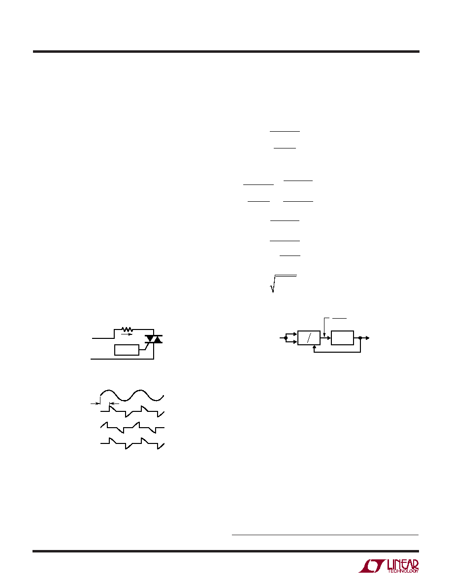
8
LTC1968
1968f
the lowpass filter. The input to the LPF is the calculation
from the multiplier/divider; (V
IN
)
2
/V
OUT
. The lowpass
filter will take the average of this to create the output,
mathematically:
APPLICATIO S I FOR ATIO
W
U
U
U
currents. The power delivered to the load depends on the
firing angle, as well as any parasitic losses such as switch
"ON" voltage drop. Real circuit waveforms will also typi-
cally have significant ringing at the switching transition,
dependent on exact circuit parasitics. For the purposes of
this data sheet, "SCR Waveforms" refers to the ideal
chopped sine wave, though the LTC1968 will do faithful
RMS-to-DC conversion with real SCR waveforms as well.
The case shown is for = 90∞, which corresponds to 50%
of available power being delivered to the load. As noted in
Table 1, when = 114∞, only 25% of the available power
is being delivered to the load and the power drops quickly
as approaches 180∞.
With an average rectification scheme and the typical
calibration to compensate for errors with sine waves, the
RMS level of an input sine wave is properly reported; it is
only with a non-sinusoidal waveform that errors occur.
Because of this calibration, and the output reading in
V
RMS
, the term True-RMS got coined to denote the use of
an actual RMS-to-DC converter as opposed to a calibrated
average rectifier.
CONTROL
V
LOAD
AC
MAINS
V
LINE
V
THY
1968 F02a
+
+
≠
+
≠
≠
I
LOAD
V
LINE
V
LOAD
V
THY
I
LOAD
1968 F02b
Figure 2a
Figure 2b
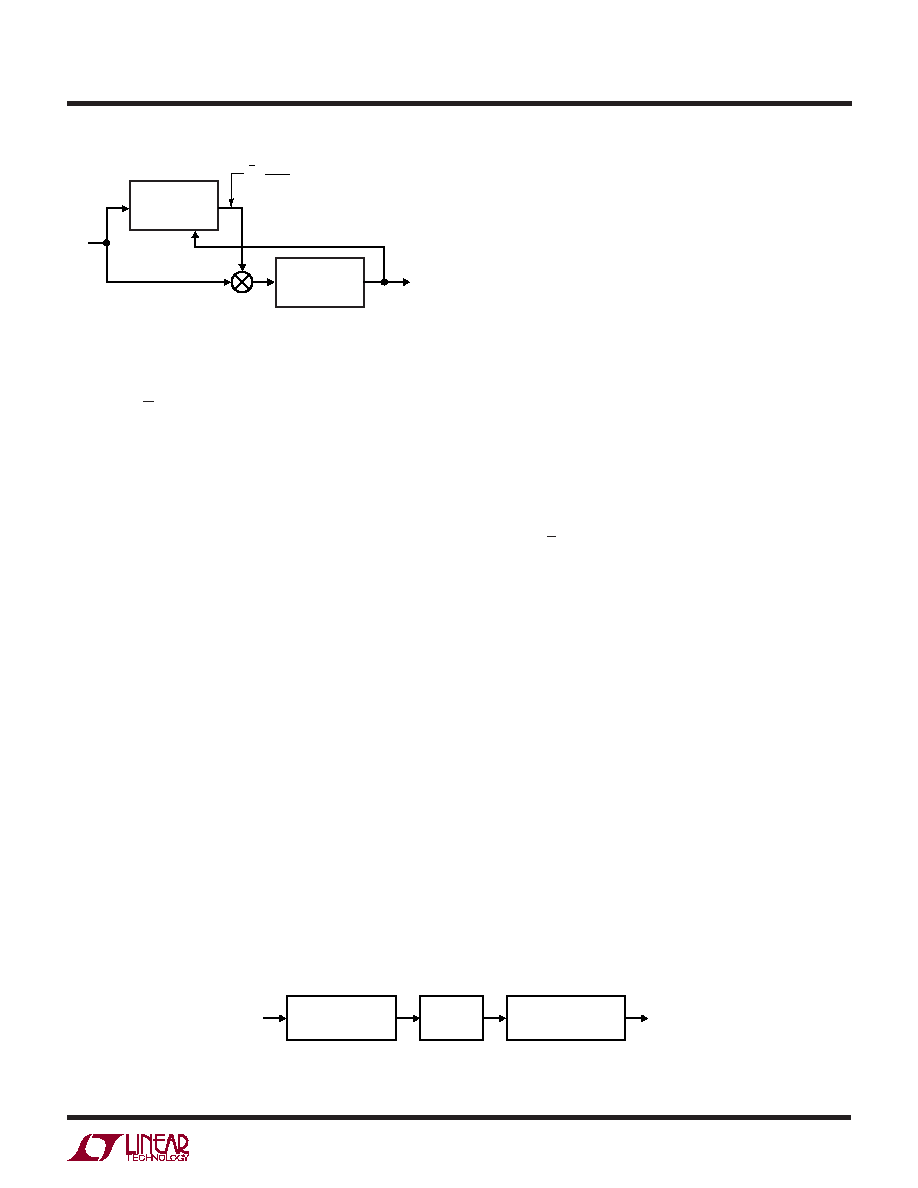
How an RMS-to-DC Converter Works
Monolithic RMS-to-DC converters use an implicit compu-
tation to calculate the RMS value of an input signal. The
fundamental building block is an analog multiply/divide
used as shown in Figure 3. Analysis of this topology is
easy and starts by identifying the inputs and the output of
V
V
V
V
V
V
so
V
V
V
and
V
V
or
V
V
RMS V
OUT
IN
OUT
OUT
IN
OUT
OUT
IN
OUT
OUT
IN
OUT
IN
IN
=
( )
( )
=
( )
=
( )
(
)
=
( )
=
( )
=
( )
2
2
2
2
2
2
2
,
,
,
,
Because V
is DC,
V
OUT
IN
Figure 3. RMS-to-DC Converter with Implicit Computation
V
IN
V
OUT
1968 F03
˜
◊
LPF
V
V
IN
OUT
( )
2
Unlike the prior generation RMS-to-DC converters, the
LTC1968 computation does NOT use log/antilog circuits,
which have all the same problems, and more, of log/
antilog multipliers/dividers, i.e., linearity is poor, the band-
width changes with the signal amplitude and the gain drifts
with temperature.
How the LTC1968 RMS-to-DC Converter Works
The LTC1968 uses a completely new topology for RMS-to-
DC conversion, in which a modulator acts as the
divider, and a simple polarity switch is used as the multi-
plier
1
as shown in Figure 4.
1
Protected by multiple patents.
9
LTC1968
1968f
APPLICATIO S I FOR ATIO
W
U
U
U
Note that the internal scalings are such that the output
duty cycle is limited to 0% or 100% only when V
IN
exceeds
±4 ∑ V
OUT
.
Linearity of an RMS-to-DC Converter
Linearity may seem like an odd property for a device that
implements a function that includes two very nonlinear
processes: squaring and square rooting.
However, an RMS-to-DC converter has a transfer func-
tion, RMS volts in to DC volts out, that should ideally have
a 1:1 transfer function. To the extent that the input to
output transfer function does not lie on a straight line, the
part is nonlinear.
A more complete look at linearity uses the simple model
shown in Figure 5. Here an ideal RMS core is corrupted by
both input circuitry and output circuitry that have imper-
fect transfer functions. As noted, input offset is introduced
in the input circuitry, while output offset is introduced in
the output circuitry.
Any nonlinearity that occurs in the output circuity will
corrupt the RMS in to DC out transfer function. A nonlin-
earity in the input circuitry will typically corrupt that
transfer function far less simply because with an AC input,
the RMS-to-DC conversion will average the nonlinearity
from a whole range of input values together.
But the input nonlinearity will still cause problems in an
RMS-to-DC converter because it will corrupt the accuracy
as the input signal shape changes. Although an RMS-to-
DC converter will convert any input waveform to a DC
output, the accuracy is not necessarily as good for all
waveforms as it is with sine waves. A common way to
describe dynamic signal wave shapes is Crest Factor. The
crest factor is the ratio of the peak value relative to the RMS
value of a waveform. A signal with a crest factor of 4, for
instance, has a peak that is four times its RMS value.
The modulator has a single-bit output whose average
duty cycle (D) will be proportional to the ratio of the input
signal divided by the output. The is a 2nd order
modulator with excellent linearity. The single-bit output is
used to selectively buffer or invert the input signal. Again,
this is a circuit with excellent linearity, because it operates
at only two points: ±1 gain; the average effective multipli-
cation over time will be on the straight line between these
two points. The combination of these two elements again
creates a lowpass filter input signal equal to (V
IN
)
2
/V
OUT
,
which, as shown above, results in RMS-to-DC conversion.
The lowpass filter performs the averaging of the RMS
function and must be a lower corner frequency than the
lowest frequency of interest. For line frequency measure-
ments, this filter is simply too large to implement on-chip,
but the LTC1968 needs only one capacitor on the output
to implement the lowpass filter. The user can select this
capacitor depending on frequency range and settling time
requirements, as will be covered in the Design Cookbook
section to follow.
This topology is inherently more stable and linear than log/
antilog implementations primarily because all of the signal
processing occurs in circuits with high gain op amps
operating closed loop.
More detail of the LTC1968 inner workings is shown in the
Simplified Schematic towards the end of this data sheet.
Figure 4. Topology of LTC1968
-
REF
V
IN
V
OUT
LPF
1968 F04
±1
D
V
V
IN
OUT
INPUT CIRCUITRY
∑ V
IOS
∑ INPUT NONLINEARITY
IDEAL
RMS-TO-DC
CONVERTER
OUTPUT CIRCUITRY
∑ V
OOS
∑ OUTPUT NONLINEARITY
INPUT
OUTPUT
1968 F05
Figure 5. Linearity Model of an RMS-to-DC Converter

10
LTC1968
1968f
Because this peak has energy (proportional to voltage
squared) that is 16 times (4
2
) the energy of the RMS value,
the peak is necessarily present for at most 6.25% (1/16)
of the time.
The LTC1968 performs very well with crest factors of 4 or
less and will respond with reduced accuracy to signals
with higher crest factors. The high performance with crest
factors less than 4 is directly attributable to the high
linearity throughout the LTC1968.
DESIGN COOKBOOK
The LTC1968 RMS-to-DC converter makes it easy to
implement a rather quirky function. For many applications
all that will be needed is a single capacitor for averaging,
appropriate selection of the I/O connections and power
supply bypassing. Of course, the LTC1968 also requires
power. A wide variety of power supply configurations are
shown in the Typical Applications section towards the end
of this data sheet.
Capacitor Value Selection
The RMS or root-mean-squared value of a signal,
the root
of the mean of the square, cannot be computed without
some averaging to obtain the
mean function. The LTC1968
true RMS-to-DC converter utilizes a single capacitor on
the output to do the low frequency averaging required for
RMS-to-DC conversion. To give an accurate measure of a
dynamic waveform, the averaging must take place over a
sufficiently long interval to average, rather than track, the
lowest frequency signals of interest. For a single averaging
capacitor, the accuracy at low frequencies is depicted in
Figure 6.
Figure 6 depicts the so-called "DC error" that results at a
given combination of input frequency and filter capacitor
values
2
. It is appropriate for most applications, in which
the output is fed to a circuit with an inherently band-limited
frequency response, such as a dual slope/integrating A/D
converter, a A/D converter or even a mechanical analog
meter.
However, if the output is examined on an oscilloscope with
a very low frequency input, the incomplete averaging will
be seen, and this ripple will be larger than the error
depicted in Figure 6. Such an output is depicted in
Figure 7. The ripple is at twice the frequency of the input
APPLICATIO S I FOR ATIO
W
U
U
U
Figure 6. DC Error vs Input Frequency
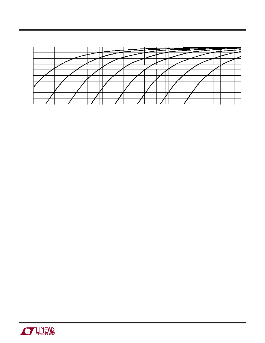
Figure 7. Output Ripple Exceeds DC Error
TIME
OUTPUT
1968 F07
DC
ERROR
(0.05%)
IDEAL
OUTPUT
DC
AVERAGE
OF ACTUAL
OUTPUT
PEAK
RIPPLE
(5%)
ACTUAL OUTPUT
WITH RIPPLE
f = 2 ◊ f
INPUT
PEAK
ERROR =
DC ERROR +
PEAK RIPPLE
(5.05%)
2
This frequency-dependent error is in additon to the static errors that affect all readings and are
therefore easy to trim or calibrate out. The "Error Analyses" section to follow discusses the effect
of static error terms.
INPUT FREQUENCY (Hz)
1
≠2.0
DC ERROR (%)
≠1.6
≠1.2
≠0.8
≠0.4
10
100
1968 F06
0
≠1.8
≠1.4
≠1.0
≠0.6
≠0.2
C = 0.22µF
C = 0.47µF
C = 1µF
C = 10µF
C = 2.2µF
C = 22µF
C = 47µF
C = 4.7µF
11
LTC1968
1968f
APPLICATIO S I FOR ATIO
W
U
U
U
because of the computation of the square of the input. The
typical values shown, 5% peak ripple with 0.05% DC error,
occur with C
AVE
= 10µF and f
INPUT
= 6Hz.
If the application calls for the output of the LTC1968 to feed
a sampling or Nyquist A/D converter (or other circuitry
that will not average out this double frequency ripple) a
larger averaging capacitor can be used. This trade-off is
depicted in Figure 8. The peak ripple error can also be
reduced by additional lowpass filtering after the LTC1968,
but the simplest solution is to use a larger averaging
capacitor.
A 10µF capacitor is a good choice for many applications.
The peak error at 50Hz/60Hz will be <1% and the DC error
will be <0.1% with frequencies of 10Hz or more.
Note that both Figure 6 and Figure 8 assume AC-coupled
waveforms with a crest factor less than 2, such as sine
waves or triangle waves. For higher crest factors and/or
AC + DC waveforms, a larger C
AVE
will generally be
required. See "Crest Factor and AC + DC Waveforms."
Capacitor Type Selection
The LTC1968 can operate with many types of capacitors.
The various types offer a wide array of sizes, tolerances,
parasitics, package styles and costs.
Ceramic chip capacitors offer low cost and small size, but
are not recommended for critical applications. The value
stability over voltage and temperature is poor with many
types of ceramic dielectrics. This will not cause an RMS-
to-DC accuracy problem except at low frequencies, where
it can aggravate the effects discussed in the previous
section. If a ceramic capacitor is used, it may be neces-
sary to use a much higher nominal value in order to
assure the low frequency accuracy desired.
Another parasitic of ceramic capacitors is leakage, which
is again dependent on voltage and particularly tempera-
ture. If the leakage is a constant current leak, the I ∑ R drop
of the leak multiplied by the output impedance of the
LTC1968 will create a constant offset of the output voltage.
If the leak is Ohmic, the resistor divider formed with the
LTC1968 output impedance will cause a gain error. For
< 0.1% gain accuracy degradation, the parallel impedance
of the capacitor leakage will need to be >1000 times the
LTC1968 output impedance. Accuracy at this level can be
hard to achieve with a ceramic capacitor, particularly with
a large value of capacitance and at high temperature.
For critical applications, a film capacitor, such as metal-
ized polyester, will be a much better choice. Although
more expensive, and larger for a given value, the value
stability and low leakage make metal-film capacitors a
trouble-free choice.
With any type of capacitor, the self-resonance of the
capacitor can be an issue with the switched capacitor
LTC1968. If the self-resonant frequency of the averaging
capacitor is 1MHz or less, a second smaller capacitor
should be added in parallel to reduce the impedance seen
by the LTC1968 output stage at high frequencies. A
capacitor 100 times smaller than the averaging capacitor
will typically be small enough to be a low cost ceramic with
a high quality dielectric such as X7R or NPO/COG.
Figure 8. Peak Error vs Input Frequency with One Cap Averaging
INPUT FREQUENCY (Hz)
1
≠1.2
PEAK ERROR (%)
≠1.0
≠0.8
≠0.6
≠0.4
10
100
1000
1968 F08
≠1.4
≠1.6
≠1.8
≠2.0
≠0.2
0
C = 220µF
C = 100µF
C = 47µF
C = 22µF
C = 10µF
C = 4.7µF
C = 2.2µF
C =1µF
12
LTC1968
1968f
Input Connections
The LTC1968 input is differential and DC coupled. The
LTC1968 responds to the RMS value of the differential
voltage between Pin 2 and Pin 3, including the DC portion
of that difference. However, there is no DC-coupled path
from the inputs to ground. Therefore, at least one of the two
inputs must be connected with a DC-return path to ground.
Both inputs must be connected to something. If either
input is left floating, a zero volt output will result.
For single-ended DC-coupled applications, simply con-
nect one of the two inputs (they are interchangeable) to
the signal, and the other to ground. This will work well for
dual supply configurations, but for single supply con-
figurations it will only work well for unipolar input sig-
nals. The LTC1968 input voltage range is from rail-to-rail,
and when the input is driven above V
+
or below GND the
gain and offset errors will increase substantially after just
a few hundred millivolts of overdrive. Fortunately, most
single supply circuits measuring a DC-coupled RMS
value will include some reference voltage other than
ground, and the second LTC1968 input can be connected
to that point.
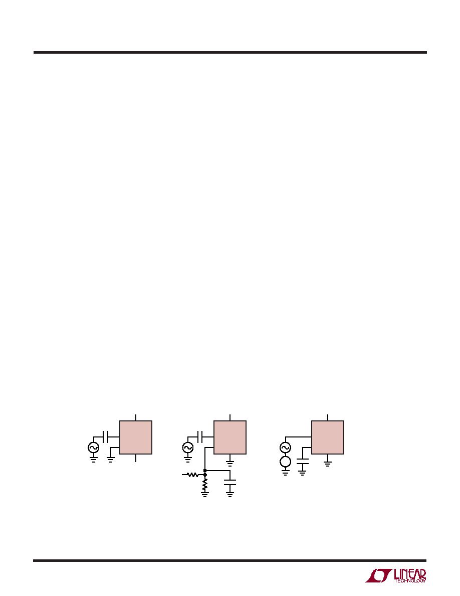
For single-ended AC-coupled applications, Figure 9 shows
three alternate topologies. The first one, shown in Figure
9a uses a coupling capacitor to one input while the other
is grounded. This will remove the DC voltage difference from
the input to the LTC1968, and it will therefore not be part
of the resulting output voltage. Again, this connection will
APPLICATIO S I FOR ATIO
W
U
U
U
work well with dual supply configurations, but in single
supply configurations it will be necessary to raise the volt-
age on the grounded input to assure that the signal at the
active input stays within the range of 0V to V
+
. If there is
already a suitable voltage reference available, connect the
second input to that point. If not, a midsupply voltage can
be created with two resistors as shown in Figure 9b.
Finally, if the input voltage is known to be between 0V and
V
+
, it can be AC coupled by using the configuration shown
in Figure 9c. Whereas the DC return path was provided
through Pin 3 in Figures 9a and 9b, in this case, the return
path is provided on Pin 2, through the input signal volt-
ages. The switched capacitor action between the two input
pins of the LTC1968 will cause the voltage on the coupling
capacitor connected to the second input to follow the DC
average of the input voltage.
For differential input applications, connect the two inputs to
the differential signal. If AC coupling is desired, one of the
two inputs can be connected through a series capacitor.
In all of these connections, to choose the input coupling
capacitor, C
C
, calculate the low frequency coupling time
constant desired, and divide by the LTC1968 differential
input impedance. Because the LTC1968 input impedance
is about 100 times its output impedance, this capacitor is
typically much smaller than the output averaging capaci-
tor. Its requirements are also much less stringent, and a
ceramic chip capacitor will usually suffice.
Figure 9. Single-Ended AC-Coupled Input Connection Alternatives
+
≠
LTC1968
GND
V
+
V
+
V
+
V
≠
(9a)
C
C
IN1
V
IN
IN2
2
3
LTC1968
(9b)
C
C
R1
10k
R2
10k
0.1µF
IN1
V
IN
V
+
IN2
2
3
LTC1968
(9c)
C
C
IN1
V
IN
1968 F09
V
DC
IN2
2
3

13
LTC1968
1968f
Output Connections
The LTC1968 output is differentially, but not symmetri-
cally, generated. That is to say, the RMS value that the
LTC1968 computes will be generated on the output (Pin 5)
relative to the output return (Pin 6), but these two pins are
not interchangeable. For most applications, Pin 6 will be
tied to ground (Pin 1). However, Pin 6 can be tied to any
voltage between 0V and V
+
(Pin 7) less the maximum
output voltage swing desired. This last restriction keeps
V
OUT
itself (Pin 5) within the range of 0V to V
+
. If a
reference level other than ground is used, it should be a
low impedance, both AC and DC, for proper operation of
the LTC1968.
In any configuration, the averaging capacitor should be
connected between Pins 5 and 6. The LTC1968 RMS-DC
output will be a positive voltage created at V
OUT
(Pin 5)
with respect to OUT RTN (Pin 6).
Power Supply Bypassing
The LTC1968 is a switched capacitor device, and large
transient power supply currents will be drawn as the
switching occurs. For reliable operation, standard power
supply bypassing must be included. A 0.01µF capacitor
from V
+
(Pin 7) to GND (Pin 1) located close to the device
will suffice. If there is a good quality ground plane avail-
able, the capacitors can go directly to that instead. Power
supply bypass capacitors can, of course, be inexpensive
ceramic types.
Up and Running!
If you have followed along this far, you should have the
LTC1968 up and running by now! Don't forget to enable
the device by grounding Pin 8, or driving it with a logic low.
Keep in mind that the LTC1968 output impedance is fairly
high, and that even the standard 10M input impedance
of a digital multimeter (DMM) or a 10◊ scope probe will load
down the output enough to degrade its typical gain error
of 0.1%. In the end application circuit, either a buffer or
another component with an extremely high input imped-
ance (such as a dual slope integrating ADC) should be used.
APPLICATIO S I FOR ATIO
W
U
U
U
For laboratory evaluation, it may suffice to use a bench-top
DMM with the ability to disconnect the 10M shunt.
If you are still having trouble, it may be helpful to skip
ahead a few pages and review the Troubleshooting Guide.
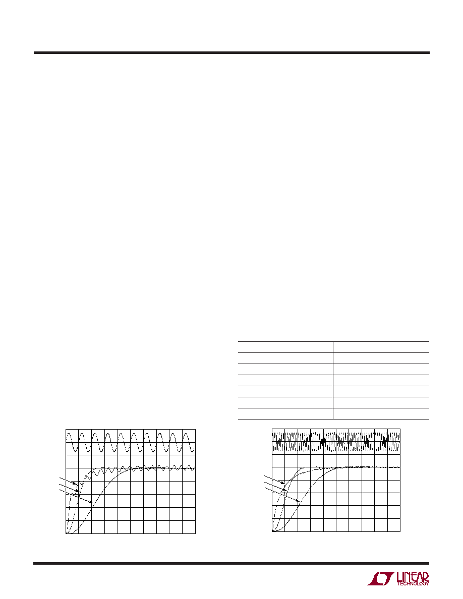
What About Response Time?
With a large value averaging capacitor, the LTC1968 can
easily perform RMS-to-DC conversion on low frequency
signals. It compares quite favorably in this regard to prior-
generation products because nothing about the
circuitry is temperature sensitive. So the RMS result
doesn't get distorted by signal driven thermal fluctuations
like a log-antilog circuit output does.
However, using large value capacitors results in a slow
response time. Figure 10 shows the rising and falling step
responses with a 10µF averaging capacitor. Although they
both appear at first glance to be standard exponential-
decay type settling, they are not. This is due to the
nonlinear nature of an RMS-to-DC calculation. Also note
the change in the time scale between the two; the rising
edge is more than twice as fast to settle to a given
accuracy. Again this is a necessary consequence of RMS-
to-DC calculation.
3
Although shown with a step change between 0mV and
100mV, the same response shapes will occur with the
LTC1968 for ANY step size. This is in marked contrast to
prior generation log/antilog RMS-to-DC converters, whose
averaging time constants are dependent on the signal
level, resulting in excruciatingly long waits for the output
to go to zero.
The shape of the rising and falling edges will be dependent
on the total percent change in the step, but for less than the
100% changes shown in Figure 10, the responses will be
less distorted and more like a standard exponential decay.
For example, when the input amplitude is changed from
3
To convince oneself of this necessity, consider a pulse train of 50% duty cycle between 0mV and
100mV. At very low frequencies, the LTC1968 will essentially track the input. But as the input
frequency is increased, the average result will converge to the RMS value of the input. If the rise and
fall characteristics were symmetrical, the output would converge to 50mV. In fact though, the RMS
value of a 100mV DC-coupled 50% duty cycle pulse train is 70.71mV, which the asymmetrical rise
and fall characteristics will converge to as the input frequency is increased.
14
LTC1968
1968f
100mV to 110mV (+10%) and back (≠10%), the step
responses are essentially the same as a standard expo-
nential rise and decay between those two levels. In such
cases, the time constant of the decay will be in between
that of the rising edge and falling edge cases of Figure 10.
Therefore, the worst case is the falling edge response as
it goes to zero, and it can be used as a design guide.
Figure 11 shows the settling accuracy vs settling time for
a variety of averaging capacitor values. If the capacitor
value previously selected (based on error requirements)
gives an acceptable settling time, your design is done.
But with 220µF, the settling time to even 10% is a full 10
seconds, which is a long time to wait. What can be done
about such a design? If the reason for choosing 220µF is
to keep the DC error with a 200mHz input less than 0.1%,
the answer is: not much. The settling time to 1% of 20
seconds is just 4 cycles of this extremely low frequency.
Averaging very low frequency signals takes a long time.
However, if the reason for choosing 220µF is to keep the
peak error with a 10Hz input less than 0.2%, there is
another way to achieve that result with a much improved
settling time.
APPLICATIO S I FOR ATIO
W
U
U
U
TIME (SEC)
0
0
OUTPUT (mV)
20
40
60
80
100
120
0.10
0.20
0.30
0.40
1968 F10a
0.50
C
AVE
= 10µF
Figure 10a. LTC1968 Rising Edge with C
AVE
= 10µF
Figure 10b. LTC1968 Falling Edge with C
AVE
= 10µF
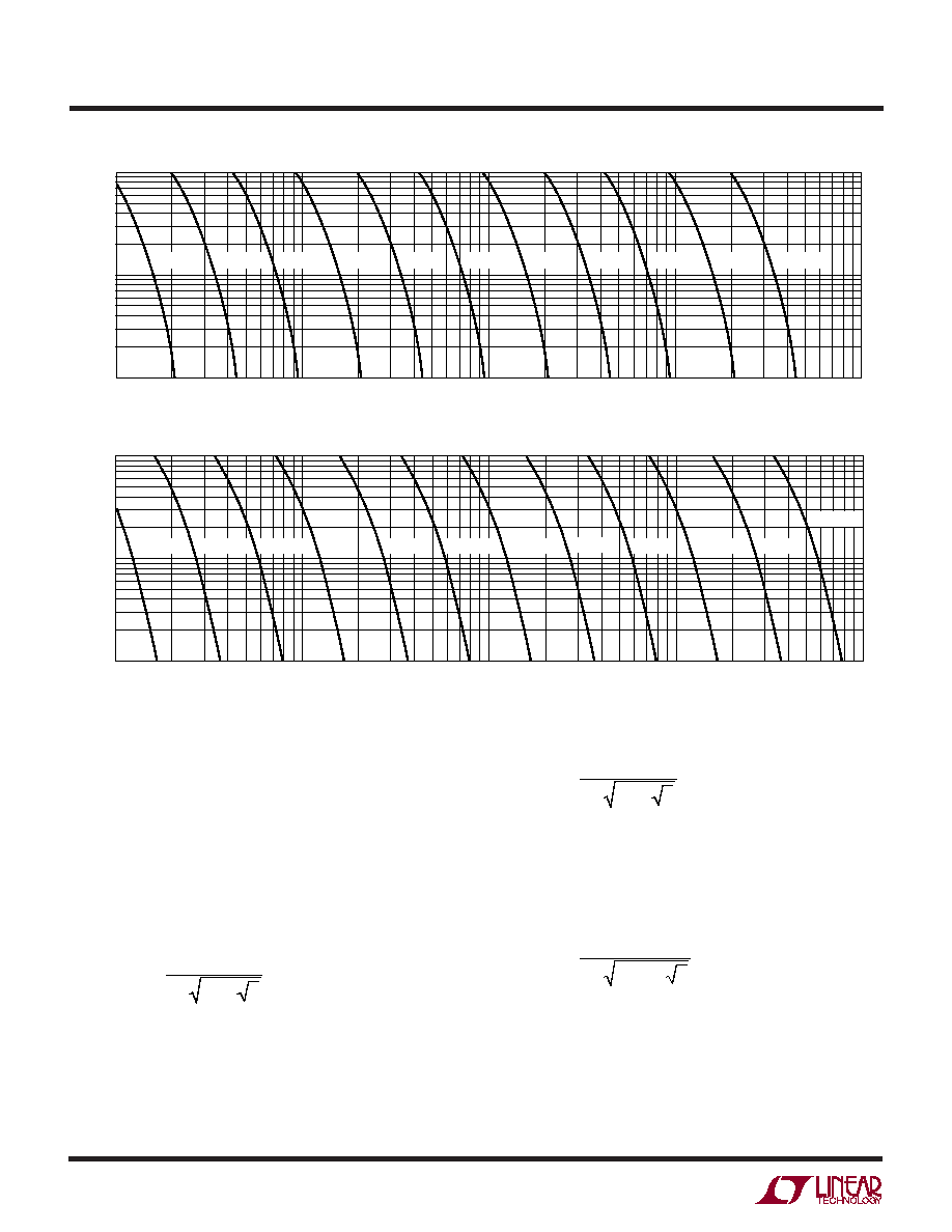
Figure 11. Settling Time vs Cap Value, One Cap Averaging
TIME (SEC)
0
0
OUTPUT (mV)
20
40
60
80
100
120
0.20
0.40
0.60
0.80
1968 F10b
1
C
AVE
= 10µF
SETTLING TIME (SEC)
0.01
0.1
SETTLING ACCURACY (%)
1
10
1
10
0.1
100
1968 F11
C = 0.1µF
C = 0.22µF C = 0.47µF C = 1µF
C = 2.2µF
C = 4.7µF
C = 10µF
C = 22µF
C = 47µF
C = 100µF
C = 220µF

15
LTC1968
1968f
Reducing Ripple with a Post Filter
The output ripple is always much larger than the DC error,
so filtering out the ripple can reduce the peak error
substantially, without the large settling time penalty of
simply increasing the averaging capacitor.
Figure 12 shows a basic 2nd order post filter, for a net 3rd
order filtering of the LTC1968 RMS calculation. It uses the
12.5k output impedance of the LTC1968 as the first re-
sistor of a 3rd order Sallen-Key active-RC filter. This topol-
ogy features a buffered output, which can be desirable
depending on the application. However, there are disad-
vantages to this topology, the first of which is that the op
amp input voltage and current errors directly degrade the
effective LTC1968 V
OOS
. The table inset in Figure 12 shows
these errors for four of Linear Technology's op amps.
A second disadvantage is that the op amp output has to
operate over the same range as the LTC1968 output, includ-
ing ground, which in single supply applications is the nega-
tive supply. Although the LTC1968 output will function fine
just millivolts from the rail, most op amp output stages (and
even some input stages) will not. There are at least two ways
to address this. First of all, the op amp can be operated split
supply if a negative supply is available. Just the op amp
would need to do so; the LTC1968 can remain single sup-
ply. A second way to address this issue is to create a signal
reference voltage a half volt or so above ground. This is most
attractive when the circuitry that follows has a differential
input, so that the tolerance of the signal reference is not a
APPLICATIO S I FOR ATIO
W
U
U
U
concern. To do this, tie all three ground symbols shown in
Figure 12 to the signal reference, as well as to the differ-
ential return for the circuitry that follows.
Figure 13 shows an alternative 2nd order post filter, for a
net 3rd order filtering of the LTC1968 RMS calculation. It
also uses the 12.5k output impedance of the LTC1968 as
the first resistor of a 3rd order active-RC filter, but this
topology filters without buffering so that the op amp DC
error characteristics do not affect the output. Although the
output impedance of the LTC1968 is increased from 12.5k
to 41.9k, this is not an issue with an extremely high input
impedance load, such as a dual-slope integrating ADC like
the ICL7106. And it allows a generic op amp to be used,
such as the SOT-23 one shown. Furthermore, it easily
works on a single supply rail by tying the noninverting
input of the op amp to a low noise reference as optionally
shown. This reference will not change the DC voltage at the
circuit output, although it does become the AC ground for
the filter, thus the (relatively) low noise requirement.
Step Responses with a Post Filter
Both of the post filters, shown in Figures 12 and 13, are
optimized for additional filtering with clean step re-
sponses. The 12.5k output impedance of the LTC1968
working into a 10µF capacitor forms a 1st order LPF with
a ≠3dB frequency of ~1.27Hz. The two filters have 10µF
at the LTC1968 output for easy comparison with a
10µF-only case, and both have the same relative Bessel-
like shape. However, because of the topological differ-
ences of pole placements between the various compo-
nents within the two filters, the net effective bandwidth
for Figure 12 is slightly higher (1.2 ∑ 1.27 1.52Hz) than
with 10µF alone, while the bandwidth for Figure 13 is
Figure 13. DC Accurate Post Filter
Figure 12. Buffered Post Filter
LTC1968
C
AVE
10µF
5
6
R1
5.6k
≠
+
R2
24.9k
R
B
C2
1µF
C1
10µF
LT1077
1968 F12
OP AMP
LTC1968 V
OOS
V
IOS
I
B/OS
∑ R
TOTAL OFFSET
R
B
VALUE
I
SQ
LT1494
±375µV
±11µV
±1.1mV
43k
1µA
LT1880
±150µV
±48µV
±940µV
SHORT
1.2mA
LT1077
±60µV
±48µV
±858µV
43k
48µA
LTC2054
±3µV
±13µV
±766µV
SHORT
150µA
±750µV
LTC1968
C
AVE
10µF
5
6
OTHER
REF VOLTAGE,
SEE TEXT
R1
29.4k
≠
+
R2
100k
C1
2.2µF
C2
2.2µF
LT1782
1068 F13
16
LTC1968
1968f
APPLICATIO S I FOR ATIO
W
U
U
U
somewhat lower (0.7 ∑ 1.27 0.9Hz) than with 10µF
alone. To adjust the bandwidth of either of them, simply
scale all the capacitors by a common multiple, and leave
the resistors unchanged.
The step responses of the LTC1968 with 10µF-only and
with the two post filters are shown in Figure 14. This is the
rising edge RMS output response to a 10Hz input starting
at t = 0. Although the falling edge response is the worst
case for settling, the rising edge illustrates the ripple that
these post filters are designed to address, so the rising
edge makes for a better intuitive comparison.
The initial rise of the LTC1968 will have enhanced slew rates
with DC and very low frequency inputs due to saturation
effects in the modulator. This is seen in Figure 14 in two
ways. First, the 10µF-only output is seen to rise very quickly
in the first 40ms. The second way this effect shows up is
that the post filter outputs have a modest overshoot, on the
order of 3mV to 4mV, or 3% to 4%. This is only an issue
with input frequency bursts at 50Hz or less, and even with
the overshoot, the settling to a given level of accuracy
improves due to the initial speedup.
As predicted by Figure 6, the DC error with 10µF is well
under 1mV and is not noticeable at this scale. However, as
predicted by Figure 8, the peak error with the ripple from
a 10Hz input is much larger, in this case about 5mV. As can
be clearly seen, the post filters reduce this ripple. Even the
wider bandwidth of Figure 12's filter is seen to cut the
ripple down substantially (to < 1mV) while the settling to
1% happens faster. With the narrower bandwidth of Figure
14's filter, the step response is somewhat slower, but the
double frequency output ripple is just 150µV.
Figure 15 shows the step response of the same three cases
with a burst of 60Hz rather than 10Hz. With 60Hz, the initial
portion of the step response is free of the boost seen in
Figure 14 and the two post-filter responses have less than
1% overshoot. The 10µF-only case still has noticeable
120Hz ripple, but both filters have removed all detectable
ripple on this scale. This is to be expected; the first order
filter will reduce the ripple about 6:1 for a 6:1 change in
frequency, while the third order filters will reduce the
ripple about 6
3
:1 or 216:1 for a 6:1 change in frequency.
Again, the two filter topologies have the same relative
shape, so the step response and ripple filtering trade-offs
of the two are the same, with the same performance of
each possible with the other by scaling it accordingly.
Figures 16 and 17 show the peak error vs. frequency for a
selection of capacitors for the two different filter topolo-
gies. To keep the clean step response, scale all three
capacitors within the filter. Scaling the buffered topology
of Figure 12 is simple because the capacitors are in a
10:1:10 ratio. Scaling the DC accurate topology of Figure
14 can be done with standard value capacitors; one decade
of scaling is shown in Table 2.
Table 2: One Decade of Capacitor Scaling for Figure 13 with EIA
Standard Values
C
AVE
C
1
= C
2
=
1µF
0.22µF
1.5µF
0.33µF
2.2µF
0.47µF
3.3µF
0.68µF
4.7µF
1µF
6.8µF
1.5µF
Figure 15. Step Responses with 60Hz Burst
Figure 14. Step Responses with 10Hz Burst
INPUT
BURST
200mV/
DIV
20mV/
DIV
10µF ONLY
FIGURE 12
FIGURE 13
STEP
RESPONSE
100ms/DIV
1968 F14
INPUT
BURST
200mV/
DIV
20mV/
DIV
10µF ONLY
FIGURE 12
FIGURE 13
STEP
RESPONSE
100ms/DIV
1968 F15

17
LTC1968
1968f
APPLICATIO S I FOR ATIO
W
U
U
U
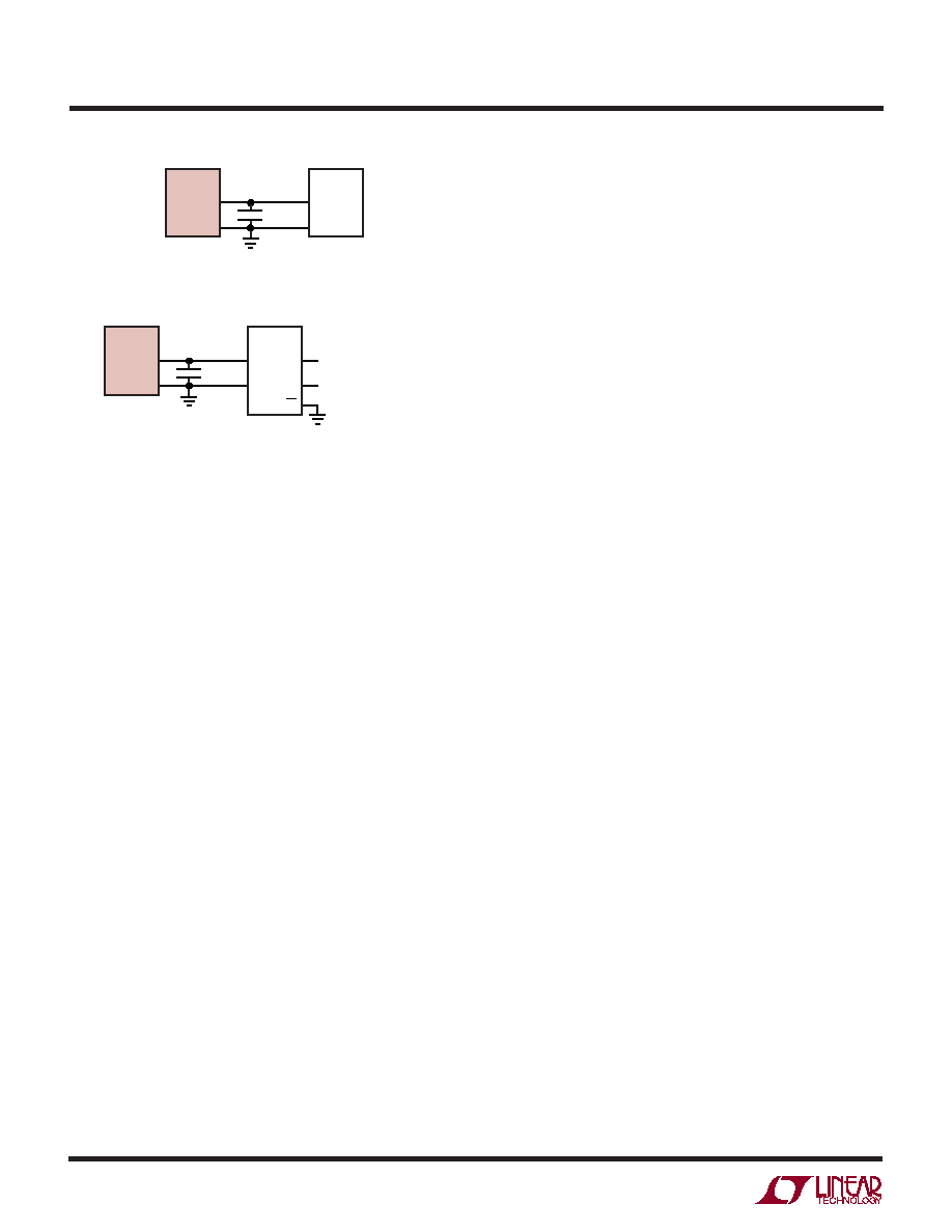
Figures 18 and 19 show the settling time versus settling
accuracy for the Buffered and DC accurate post filters,
respectively. The different curves represent different
scalings of the filters, as indicated by the C
AVE
value. These
are comparable to the curves in Figure 11 (single capacitor
case), with somewhat less settling time for the buffered
post filter, and somewhat more settling time for the
DC-accurate post filter. These differences are due to the
change in overall bandwidth as mentioned earlier.
Although the settling times for the post-filtered configura-
tions shown on Figures 18 and 19 are not that much
different from those with a single capacitor, the point of
using a post filter is that the settling times are far better for
a given level peak error. The filters dramatically reduce the
low frequency averaging ripple with far less impact on
settling time.
Crest Factor and AC + DC Waveforms
In the preceding discussion, the waveform was assumed
to be AC coupled, with a modest crest factor. Both
assumptions ease the requirements for the averaging
capacitor. With an AC-coupled sine wave, the calculation
engine squares the input, so the averaging filter that
follows is required to filter twice the input frequency,
making its job easier. But with a sinewave that includes
DC offset, the square of the input has frequency content
at the input frequency and the filter must average out that
lower frequency. So with AC + DC waveforms, the re-
quired value for C
AVE
should be based on half of the lowest
input frequency, using the same design curves presented
in Figures 6, 8, 16 and 17.
Figure 17. Peak Error vs Input Frequency with DC-Accurate Post Filter
Figure 16. Peak Error vs Input Frequency with Buffered Post Filter
INPUT FREQUENCY (Hz)
1
≠1.2
PEAK ERROR (%)
≠1.0
≠0.8
≠0.6
≠0.4
10
100
1000
1968 F08
≠1.4
≠1.6
≠1.8
≠2.0
≠0.2
0
C = 22µF
C = 100µF
C = 47µF
C = 10µF
C = 4.7µF
C = 2.2µF
C = 0.47µF
C = 0.22µF
C = 0.1µF
C =1µF
INPUT FREQUENCY (Hz)
1
≠1.2
PEAK ERROR (%)
≠1.0
≠0.8
≠0.6
≠0.4
10
100
1000
1968 F08
≠1.4
≠1.6
≠1.8
≠2.0
≠0.2
0
C = 22µF
C = 47µF
C = 10µF
C = 4.7µF
C = 2.2µF
C = 0.47µF
C = 0.22µF
C = 0.1µF
C = 0.047µF
C =1µF
18
LTC1968
1968f
APPLICATIO S I FOR ATIO
W
U
U
U
Crest factor, which is the peak to RMS ratio of a dynamic
signal, also effects the required C
AVE
value. With a higher
crest factor, more of the energy in the signal is concentrated
into a smaller portion of the waveform, and the averaging
has to ride out the long lull in signal activity. For busy
waveforms, such as a sum of sine waves, ECG traces or
SCR-chopped sine waves, the required value for C
AVE
should be based on the lowest fundamental input frequency
divided as such:
f
f
CF
DESIGN
INPUT MIN
=
(
)
∑
≠
3
2
using the same design curves presented in Figures 6, 8,
16 and 17. For the worst case of square top pulse trains,
that are always either zero volts or the peak voltage, base
the selection on the lowest fundamental input frequency
divided by twice as much:
f
f
CF
DESIGN
INPUT MIN
=
(
)
∑
≠
6
2
The effects of crest factor and DC offsets are cumulative.
So for example, a 10% duty cycle pulse train from 0V
PEAK
to 1V
PEAK
(CF = 10 = 3.16) repeating at 16.67ms (60Hz)
input is effectively only 30Hz due to the DC asymmetry and
is effectively only:
f
Hz
DESIGN
=
=
30
6
3 16
2
3 78
∑
.
≠
.
for the purposes of Figures 6, 8, 16 and 17.
Obviously, the effect of crest factor is somewhat simplified
above given the factor of two difference based on a
subjective description of the waveform type. The results
will vary somewhat based on actual crest factor and
Figure 19. Settling Time with DC-Accurate Post Filter
Figure 18. Settling Time with Buffered Post Filter
SETTLING TIME (SEC)
0.01
0.1
SETTLING ACCURACY (%)
1
10
1
0.1
10
100
1968 F18
C = 0.22µF
C = 0.47µF
C = 1µF
C = 2.2µF
C = 4.7µF
C = 10µF
C = 22µF
C = 47µF
C = 100µF
C = 220µF
C = 470µF
SETTLING TIME (SEC)
0.01
0.1
SETTLING ACCURACY (%)
1
10
1
0.1
10
100
1968 F19
C = 0.1µF
C = 0.22µF
C = 0.47µF
C = 1µF
C = 2.2µF
C = 4.7µF
C = 10µF
C = 22µF
C = 47µF
C = 100µF
C = 220µF
C = 470µF

19
LTC1968
1968f
waveform dynamics and the type of filtering used. The
above method is conservative for some cases and about
right for others.
The LTC1968 works well with signals whose crest factor
is 4 or less. At higher crest factors, the internal
modulator will saturate, and results will vary depending on
the exact frequency, shape and (to a lesser extent) ampli-
tude of the input waveform. The output voltage could be
higher or lower than the actual RMS of the input signal.
The modulator may also saturate when signals with
crest factors less than 4 are used with insufficient averag-
ing. This will only occur when the output droops to less
than 1/4 of the input voltage peak. For instance, a DC-
coupled pulse train with a crest factor of 4 has a duty cycle
of 6.25% and a 1V
PEAK
input is 250mV
RMS
. If this input is
50Hz, repeating every 20ms, and C
AVE
= 10µF, the output
will droop during the inactive 93.75% of the waveform.
This droop is calculated as:
V
V
e
MIN
RMS
INACTIVE TIME
=
-
2
1≠
2 ∑ Z
∑ C
OUT
AVE
For the LTC1968, whose output impedance (Z
OUT
) is
12.5k, this droop works out to ≠ 3.6%, so the output
would be reduced to 241mV at the end of the inactive
portion of the input. When the input signal again climbs to
1V
PEAK
, the peak/output ratio is 4.15.
With C
AVE
= 100µF, the droop is only ≠ 0.37% to 249.1mV
and the peak/output ratio is just 4.015, which the LTC1968
has enough margin to handle without error.
For crest factors less than 3.5, the selection of C
AVE
as
previously described should be sufficient to avoid this
droop and modulator saturation effect. But with crest
factors above 3.5, the droop should also be checked for
each design.
Error Analyses
Once the RMS-to-DC conversion circuit is working, it is
time to take a step back and do an analysis of the accuracy
of that conversion. The LTC1968 specifications include
three basic static error terms, V
OOS
, V
IOS
and GAIN. The
output offset is an error that simply adds to (or subtracts
APPLICATIO S I FOR ATIO
W
U
U
U
from) the voltage at the output. The conversion gain of the
LTC1968 is nominally 1.000 V
DCOUT
/V
RMSIN
and the gain
error reflects the extent to which this conversion gain is
not perfectly unity. Both of these affect the results in a
fairly obvious way.
Input offset on the other hand, despite its conceptual
simplicity, effects the output in a nonobvious way. As its
name implies, it is a constant error voltage that adds
directly with the input. And it is the sum of the input and
V
IOS
that is RMS converted.
This means that the effect of V
IOS
is warped by the
nonlinear RMS conversion. With 0.4mV (typ) V
IOS
, and a
200mV
RMS
AC input, the RMS calculation will add the DC
and AC terms in an RMS fashion and the effect is
negligible:
V
OUT
= (200mV AC)
2
+ (0.4mV DC)
2
= 200.0004mV
= 200mV + 2ppm
But with 10◊ less AC input, the error caused by V
IOS
is
100◊ larger:
V
OUT
= (20mV AC)
2
+ (0.4mV DC)
2
= 20.004mV
= 20mV + 200ppm
This phenomena, although small, is one source of the
LTC1968's residual nonlinearity.
On the other hand, if the input is DC coupled, the input
offset voltage adds directly. With +200mV and a +0.4mV
V
IOS
, a 200.4mV output will result, an error of 0.2% or
2000ppm. With DC inputs, the error caused by V
IOS
can be
positive or negative depending if the two have the same or
opposing polarity.
The total conversion error with a sine wave input using the
typical values of the LTC1968 static errors is computed as
follows:
V
OUT
= ((500mV AC)
2
+ (0.4mV DC)
2
) ∑ 1.001 + 0.2mV
= 500.700mV
= 500mV + 0.140%
V
OUT
= ((50mV AC)
2
+ (0.4mV DC)
2
) ∑ 1.001 + 0.2mV
= 50.252mV
= 50mV + 0.503%

20
LTC1968
1968f
V
OUT
= ((5mV AC)
2
+ (0.4mV DC)
2
) ∑ 1.001 + 0.2mV
= 5.221mV
= 5mV + 4.42%
As can be seen, the gain term dominates with large inputs,
while the offset terms become significant with smaller
inputs. In fact, 5mV is the minimum RMS level needed to
keep the LTC1968 calculation core functioning normally,
so this represents the worst-case of usable input levels.
Using the worst-case values of the LTC1968 static errors,
the total conversion error is:
V
OUT
= ((500mV AC)
2
+ (1.5mV DC)
2
) ∑ 1.003 + 0.75mV
= 502.25mV
= 500mV + 0.45%
V
OUT
= ((50mV AC)
2
+ (1.5mV DC)
2
) ∑ 1.003 + 0.75mV
= 50.923mV
= 50mV + 1.85%
V
OUT
= ((5mV AC)
2
+ (1.5mV DC)
2
) ∑ 1.003 + 0.75mV
= 5.986mV
= 5mV + 19.7%
These static error terms are in addition to dynamic error
terms that depend on the input signal. See the Design
Cookbook for a discussion of the DC conversion error with
low frequency AC inputs. The LTC1968 bandwidth limita-
tions cause additional errors with high frequency inputs.
Another dynamic error is due to crest factor. The LTC1968
performance versus crest factor is shown in the Typical
Performance Characteristics.
Output Errors Versus Frequency
As mentioned in the design cookbook, the LTC1968 per-
forms very well with low frequency and very low frequency
inputs, provided a large enough averaging capacitor is used.
However, the LTC1968 will have additional dynamic errors
as the input frequency is increased. The LTC1968 is de-
signed for high accuracy RMS-to-DC conversion of sig-
nals up to 100kHz. However, the switched capacitor cir-
cuitry samples the inputs at a modest 2MHz nominal. The
response versus frequency is depicted in the Typical Per-
formance Characteristics titled Input Signal Bandwidth.
APPLICATIO S I FOR ATIO
W
U
U
U
Although there is a pattern to the response versus fre-
quency that repeats every sample frequency, the errors
are not overwhelming. This is because LTC1968 RMS
calculation is inherently wideband, operating properly with
minimal oversampling, or even undersampling, using sev-
eral proprietary techniques to exploit the fact that the RMS
value of an aliased signal is the same as the RMS value of
the original signal. However, a fundamental feature of the
modulator is that sample estimation noise is shaped
such that minimal noise occurs with input frequencies
much less than the sampling frequency, but such noise
peaks when input frequency reaches half the sampling
frequency. Fortunately the LTC1968 output averaging fil-
ter greatly reduces this error, but the RMS-to-DC topology
frequency shifts the noise to low (baseband) frequencies.
See Output Noise vs Input Frequency in the Typical Perfor-
mance Characteristics.
Input Impedance
The LTC1968 true RMS-to-DC converter utilizes a 0.8pF
capacitor to sample the input at a nominal 2MHz sample
frequency. This accounts for the 1.2M input impedance.
See Figure 20 for the equivalent analog input circuit. Note
however, that the 1.2M input impedance does not di-
rectly affect the input sampling accuracy. For instance, if
a 15.5k source resistance is used to drive the LTC1968, the
sampling action of the input stage will drag down the
voltage seen at the input pins with small spikes at every
sample clock edge as the sample capacitor is connected to
be charged. The time constant of this combination is
small, 0.8pF ∑ 15.5k = 12.5ns, and during the 125ns
period devoted to sampling, ten time constants elapse.
Figure 20. LTC1968 Equivalent Analog Input Circuit
IN1
V
DD
V
DD
V
SS
V
SS
R
SW
(TYP)
2k
C
EQ
0.8pF
(TYP)
C
EQ
0.8pF
(TYP)
I
IN1
IN2
I
IN2
1968 F20
R
SW
(TYP)
2k
I IN
V
V
R
I IN
V
V
R
R
M
AVG
IN
IN
EQ
AVG
IN
IN
EQ
EQ
1
2
1.2
1
2
2
1
( )
=
-
( )
=
-
=

21
LTC1968
1968f
APPLICATIO S I FOR ATIO
W
U
U
U
This allows each sample to settle to within 46ppm and it is
these samples that are used to compute the RMS value.
This is a much higher accuracy than the LTC1968 conver-
sion limits, and far better than the accuracy computed via
the simplistic resistive divider model:
Output Impedance
The LTC1968 output impedance during operation is simi-
larly due to a switched capacitor action. In this case, 20pF
of on-chip capacitance operating at 2MHz translates into
25k. The closed-loop RMS-to-DC calculation cuts that in
half to the nominal 12.5k specified.
In order to create a DC result, a large averaging capacitor
is required. Capacitive loading and time constants are not
an issue on the output.
However, resistive loading is an issue and the 10M
impedance of a DMM or 10◊ scope probe will drag the
output down by ≠0.125% typ.
During shutdown, the switching action is halted and a
fixed 12.5k resistor shunts V
OUT
to OUT RTN so that C
AVE
is discharged.
Interfacing with an ADC
The LTC1968 output impedance and the RMS averaging
ripple need to be considered when using an analog-to-
digital converter (ADC) to digitize the LTC1968 RMS
result.
The simplest configuration is to connect the LTC1968
directly to the input of a type 7106/7136 ADC as shown in
Figure 21a. These devices are designed specifically for
DVM/DPM use and include display drivers for a 3 1/2 digit
LCD segmented display. Using a dual-slope conversion,
the input is sampled over a long integration window, which
results in rejection of line frequency ripple when integra-
tion time is an integer number of line cycles. Finally, these
parts have an input impedance in the G range, with
specified input leakage of 10pA to 20pA. Such a leakage,
combined with the LTC1968 output impedance, results in
less than 1µV of additional output offset voltage.
Another type of ADC that has inherent rejection of RMS
averaging ripple is an oversampling ADC such as the
LTC2420. Its input impedance is 6.5M, but only when it
is sampling. Since this occurs only half the time at most,
if it directly loads the LTC1968, a gain error of ≠0.08% to
≠0.11% results. In fact, the LTC2420 DC input current is
V
V
R
R
R
V
M
V
IN
SOURCE
IN
IN
SOURCE
SOURCE
SOURCE
=
+
=
=
1.2
1 25
≠ .
%
M
k
+
1.2
15.5
This resistive divider calculation does give the correct
model of what voltage is seen at the input terminals by a
parallel load averaged over a several clock cycles, which is
what a large shunt capacitor will do--average the current
spikes over several clock cycles.
When high source impedances are used, care must be taken
to minimize shunt capacitance at the LTC1968 input so as
not to increase the settling time. Shunt capacitance of just
0.8pF will double the input settling time constant and the
error in the above example grows from 46ppm to 0.67%
(6700ppm). As a consequence, it is important to
not try to
filter the input with large input capacitances unless driven
by a low impedance. Keep time constant << 125ns.
When the LTC1968 is driven by op amp outputs, whose
low DC impedance can be compromised by sharp capaci-
tive load switching, a small series resistor may be added.
A 1k resistor will easily settle with the 0.8pF input sampling
capacitor to within 1ppm.
These are important points to consider both during design
and debug. During lab debug, and even production testing,
a high value series resistor to any test point is advisable.
22
LTC1968
1968f
not zero at 0V, but rather at one half its reference, so both
an output offset and a gain error will result. These errors
will vary from part to part, but with a specific LTC1968 and
LTC2420 combination, the errors will be fixed, varying less
than ±0.05% over temperature. So a system that has digi-
tal calibration can be quite accurate despite the nominal
gain and offset error. With 20 bits of resolution, this part
is more accurate than the LTC1968, but the extra resolu-
tion is helpful because it reduces nonlinearity at the LSB
transitions as a digital gain correction is made. Further-
more, its small size and ease of use make it attractive.
This connection is shown in Figure 21b, where the LTC2420
is set to continuously convert by grounding the CS pin. The
gain error will be less if CS is driven at a slower rate,
however, the rate should either be consistent or at a rate
low enough that the LTC1968 and its output capacitor have
fully settled by the beginning of each conversion, so that
the loading errors are consistent.
Other types of ADCs sample the input signal once and
perform a conversion on that one sample. With these
ADCs (Nyquist ADCs), a post filter will be needed in most
cases to reduce the peak error with low input frequencies.
The DC-accurate filter of Figure 13 is attractive from an
error standpoint, but it increases the impedance at the ADC
input. In most cases, the buffered post filter of Figure 12
will be more appropriate for use with Nyquist analog-to-
digital converters.
SYSTEM CALIBRATION
The LTC1968 static accuracy can be improved with end-
system calibration. Traditionally, calibration has been
done at the factory, or at a service depot only, typically
using manually adjusted potentiometers. Increasingly,
systems are being designed for electronic calibration
where the accuracy corrections are implemented in digital
code wherever possible, and with calibration DACs where
necessary. Additionally, many systems are now designed
for self calibration, in which the calibration occurs inside
the machine, automatically without user intervention.
Whatever calibration scheme is used, the linearity of the
LTC1968 will improve the calibrated accuracy over that
achievable with older log/antilog RMS-to-DC converters.
Additionally, calibration using DC reference voltages are
essentially as accurate with the LTC1968 as those using
AC reference voltages. Older log/antilog RMS-to-DC con-
verters required nonlinear input stages (rectifiers) whose
linearity would typically render DC-based calibration
unworkable.
The following are four suggested calibration methods.
Implementations of the suggested adjustments are de-
pendent on the system design, but in many cases, gain and
output offset can be corrected in the digital domain, and
will include the effect of all gains and offsets from the
LTC1968 output through the ADC. Input offset voltage, on
the other hand, will have to be corrected with adjustment
to the actual analog input to the LTC1968.
AC-Only, 1 Point
The dominant error at full scale will be caused by the gain
error, and by applying a full-scale sine wave input, this
error can be measured and corrected for. Unlike older log/
antilog RMS-to-DC converters, the correction should be
made for zero error at full scale to minimize errors through-
out the dynamic range.
The best frequency for the calibration signal is roughly ten
times the ≠0.1% DC error frequency. For 10µF, ≠0.1% DC
error occurs at 6Hz, so 60Hz is a good calibration frequency,
although anywhere from 60Hz to 100Hz should suffice.
APPLICATIO S I FOR ATIO
W
U
U
U
Figure 21a. Interfacing to DVM/DPM ADC
Figure 21b. Interfacing to LTC2420
C
AVE
LTC1968
OUTPUT
OUT RTN
7106 TYPE
IN HI
IN LO
5
6
31
1968 F21a
30
C
AVE
LTC1968
OUTPUT
OUT RTN
LTC2420
V
IN
SERIAL
DATA
DIGITALLY CORRECT
LOADING ERRORS
GND
SDO
SCK
CS
5
6
3
1968 F21b
4

23
LTC1968
1968f
The trade-off here is that on the one hand, the DC error is
input frequency dependent, so a calibration signal fre-
quency high enough to make the DC error negligible
should be used. On the other hand, as low a frequency as
can be used is best to avoid attenuation of the calibrated
AC signal, either from parasitic RC loading or insufficient
op amp gain. For instance, with a 1kHz calibration signal,
a 1MHz op amp will typically only have 60dB of open-loop
gain, so it could attenuate the calibration signal a full 0.1%.
AC-Only, 2 Point
The next most significant error for AC-coupled applica-
tions will be the effect of output offset voltage, noticeable
at the bottom end of the input scale. This too can be
calibrated out if two measurements are made, one with a
full-scale sine wave input and a second with a sine wave
input (of the same frequency) at 10% of full scale. The
trade-off in selecting this second level is that it should be
small enough that the gain error effect becomes small
compared to the gain error effect at full scale, while on the
other hand, not using so small an input that the input offset
voltage becomes an issue.
The calculations of the error terms for a 200mV full-scale
case are:
Gain =
Reading at 200mV ≠ Reading at 20mV
180mV
Output Offset =
Reading at 20mV
Gain
≠ 20mV
DC, 2 Point
DC-based calibration is preferable in many cases because
a DC voltage of known, good accuracy is easier to gener-
ate than such an AC calibration voltage. The only down
side is that the LTC1968 input offset voltage plays a role.
It is therefore suggested that a DC-based calibration
scheme check at least two points: ±full scale. Applying the
≠full-scale input can be done by physically inverting the
voltage or by applying the same +full-scale input to the
opposite LTC1968 input.
For an otherwise AC-coupled application, only the gain
term may be worth correcting for, but for DC-coupled
applications, the input offset voltage can also be calcu-
lated and corrected for.
The calculations of the error terms for a 200mV full-scale
case are:
Gain =
Reading at 200mV + Reading at ≠ 200mV
400mV
Input Offset =
Reading at ≠ 200mV ≠ Reading at 200mV
2 ∑Gain
Note: Calculation of and correction for input offset voltage
are the only way in which the two LTC1968 inputs (IN1,
IN2) are distinguishable from each other. The calculation
above assumes the standard definition of offset; that a
positive offset is the case of a positive voltage error inside
the device that must be corrected by applying a like
negative voltage outside. The offset is referred to which-
ever pin is driven positive for the +full-scale reading.
DC, 3 Point
One more point is needed with a DC calibration scheme to
determine output offset voltage: +10% of full scale.
The calculation of the input offset is the same as for the
2-point calibration above, while the gain and output offset
are calculated for a 200mV full-scale case as:
Gain =
Reading at 200mV ≠ Reading at 20mV
180mV
Output Offset =
Reading at 200mV +Reading at ≠ 200mV ≠ 400mV ∑ Gain
2
APPLICATIO S I FOR ATIO
W
U
U
U
24
LTC1968
1968f
APPLICATIO S I FOR ATIO
W
U
U
U
TROUBLESHOOTING GUIDE
Top Ten LTC1968 Application Mistakes
1. Circuit won't work≠Dead On Arrival≠no power drawn.
≠ Probably forgot to enable the LTC1968 by pulling
Pin 8 low.
Solution: Tie Pin 8 to Pin 1.
2. Circuit won't work, but draws power. Zero or very
little output, single-ended input application.
≠ Probably didn't connect both input pins.
Solution: Tie both inputs to something. See "Input
Connections" in the Design Cookbook.
4. Gain is low by a few percent, along with other screwy
results.
≠ Probably tried to use output in a floating, differential
manner.
Solution: Tie Pin 6 to a low impedance. See "Output
Connections" in the Design Cookbook.
LTC1968
CONNECT PIN 3
IN1
2
3
NC
IN2
1968TS02
LTC1968
IN1
2
3
IN2
1968 TS03
DC-COUPLE ONE INPUT
LTC1968
DC-CONNECT ONE INPUT
IN1
2
3
IN2
3. Screwy results, particularly with respect to linearity
or high crest factors; differential input application.
≠ Probably AC-coupled both input pins.
Solution: Make at least one input DC-coupled. See
"Input Connections" in the Design Cookbook.
TYPE 7136
ADC
LTC1968
HI
31
30
5
6
LO
V
OUT
OUT RTN
1968 TS04
GROUND PIN 6
5. Offsets perceived to be out of specification because 0V
in 0V out.
≠ The offsets are not specified at 0V in. No RMS-to-
DC converter works well at 0 due to a divide-by-zero
calculation.
Solution: Measure V
IOS
/V
OOS
by extrapolating read-
ings > ±5mV
DC
.
6. Linearity perceived to be out of specification particu-
larly with small input signals.
≠ This could again be due to using 0V in as one of the
measurement points.
Solution: Check Linearity from 5mV
RMS
to
500mV
RMS
.
≠ The input offset voltage can cause small AC linear
ityerrors at low input amplitudes as well. See "Error
Analyses" section.
Possible Solution: Include a trim for input offset.
25
LTC1968
1968f
APPLICATIO S I FOR ATIO
W
U
U
U
7. Output is noisy with >200kHz inputs.
≠ This is a fundamental characteristic of this topol-
ogy. The LTC1968 is designed to work very well
with inputs of 100kHz or less. It works okay as high
as 1MHz, but it is limited by aliased noise.
Solution: Bandwidth limit the input or digitally filter
the resulting output.
8. Large errors occur at crest factors approaching, but
less than 4.
≠ Insufficient averaging.
Solution: Increase C
AVE
. See "Crest Factor and AC +
DC Waveforms" section for discussion of output
droop.
9. Screwy results, errors > spec limits, typically 1% to 5%.
≠ High impedance (12.5k) and high accuracy (0.1%)
require clean boards! Flux residue, finger grime, etc.
all wreak havoc at this level.
Solution: Wash the board.
10. Gain is low by 1% or more, no other problems.
≠ Probably due to circuit loading. With a DMM or a
10◊ scope probe, Z
IN
= 10M. The LTC1968
output is 12.5k, resulting in ≠ 0.125% gain
error. Output impedance is higher with the DC
accurate post filter.
Solution: Remove the shunt loading or buffer the
output.
≠ Loading can also be caused by cheap averaging
capacitors.
Solution: Use a high quality metal film capacitor
for C
AVE
.
LTC1968
KEEP BOARD CLEAN
1968 TS09
200mV
RMS
IN
≠0.125%
DMM
DCV
LTC1968
10M
5
12.5k
6
V
OUT
OUT RTN
1968 TS10
LOADING DRAGS DOWN GAIN
mV
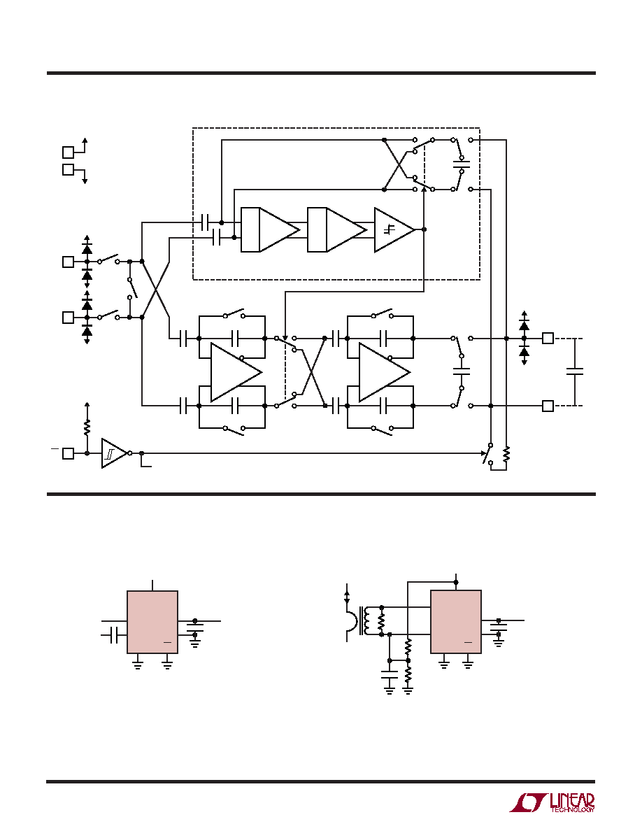
26
LTC1968
1968f
TYPICAL APPLICATIO S
U
SI PLIFIED SCHE ATIC
W
W
5V Single Supply, Differential,
AC-Coupled RMS-to-DC Converter
Single Supply RMS Current Measurement
V
+
5V
LTC1968
IN1
DC OUTPUT
C
AVE
10µF
C
C
1µF
IN2
1968 TA02
V
OUT
AC INPUTS
(1V
PEAK
DIFFERENTIAL)
OUT RTN
GND
EN
V
+
LTC1968
IN1
V
OUT
= 4mV
DC
/A
RMS
C
AVE
10µF
0.1µF
IN2
1968 TA03
V
OUT
AC CURRENT
75A MAX
50Hz TO 400Hz
OUT RTN
GND
EN
10k
10k
10
T1: CR MAGNETICS CR8348-2500-N
www.crmagnetics.com
T1
2nd ORDER MODULATOR
IN1
IN2
EN
V
+
≠
+
≠
+
OUTPUT
OUT RTN
50k
BLEED RESISTOR
FOR C
AVE
C
AVE
1968 SS
TO BIAS CONTROL
GND
C1
C2
Y1
Y2
C12
C11
CLOSED
DURING
SHUTDOWN
C9
C10
C5
C3
C4
C6
C8
C7
A2
A1

27
LTC1968
1968f
U
PACKAGE DESCRIPTIO
MS8 Package
8-Lead Plastic MSOP
(Reference LTC DWG # 05-08-1660)
Information furnished by Linear Technology Corporation is believed to be accurate and reliable.
However, no responsibility is assumed for its use. Linear Technology Corporation makes no represen-
tation that the interconnection of its circuits as described herein will not infringe on existing patent rights.
TYPICAL APPLICATIO S
U
±2.5V Supplies, Single Ended, DC-Coupled
RMS-to-DC Converter with Shutdown
RMS Noise Measurement
V
+
2.5V
≠2.5V
≠2.5V
LTC1968
IN1
DC OUTPUT
C
AVE
10µF
0.1µF
X7R
IN2
1968 TA04
V
OUT
DC + AC
INPUT
(1V
PEAK
)
OUT RTN
GND
EN
OFF
2V
≠2V
ON
V
+
2.5V
≠2.5V
2.5V
≠2.5V
LTC1968
IN1
C
AVE
10µF
0.1µF
1.5µF
IN2
1968 TA05
V
OUT
VOLTAGE
NOISE IN
OUT RTN
GND
EN
1mV
DC
1µV
RMS
OF INPUT NOISE
V
OUT
=
≠
+
1k
100
100
100k
BW 1kHz TO 100kHz
INPUT SENSITIVITY = 1µV
RMS
TYP
1/2
LTC6203
MSOP (MS8) 0204
0.53 ± 0.152
(.021 ± .006)
SEATING
PLANE
NOTE:
1. DIMENSIONS IN MILLIMETER/(INCH)
2. DRAWING NOT TO SCALE
3. DIMENSION DOES NOT INCLUDE MOLD FLASH, PROTRUSIONS OR GATE BURRS.
MOLD FLASH, PROTRUSIONS OR GATE BURRS SHALL NOT EXCEED 0.152mm (.006") PER SIDE
4. DIMENSION DOES NOT INCLUDE INTERLEAD FLASH OR PROTRUSIONS.
INTERLEAD FLASH OR PROTRUSIONS SHALL NOT EXCEED 0.152mm (.006") PER SIDE
5. LEAD COPLANARITY (BOTTOM OF LEADS AFTER FORMING) SHALL BE 0.102mm (.004") MAX
0.18
(.007)
0.254
(.010)
1.10
(.043)
MAX
0.22 ≠ 0.38
(.009 ≠ .015)
TYP
0.127 ± 0.076
(.005 ± .003)
0.86
(.034)
REF
0.65
(.0256)
BSC
0∞ ≠ 6∞ TYP
DETAIL "A"
DETAIL "A"
GAUGE PLANE
1
2
3
4
4.90 ± 0.152
(.193 ± .006)
8
7 6 5
3.00 ± 0.102
(.118 ± .004)
(NOTE 3)
3.00 ± 0.102
(.118 ± .004)
(NOTE 4)
0.52
(.0205)
REF
5.23
(.206)
MIN
3.20 ≠ 3.45
(.126 ≠ .136)
0.889 ± 0.127
(.035 ± .005)
RECOMMENDED SOLDER PAD LAYOUT
0.42 ± 0.038
(.0165 ± .0015)
TYP
0.65
(.0256)
BSC

28
LTC1968
1968f
© LINEAR TECHNOLOGY CORPORATION 2004
LT/TP 0604 1K ∑ PRINTED IN USA
Linear Technology Corporation
1630 McCarthy Blvd., Milpitas, CA 95035-7417
(408) 432-1900
FAX: (408) 434-0507
www.linear.com
RELATED PARTS
PART NUMBER
DESCRIPTION
COMMENTS
LT
Æ
1077
Micropower, Single Supply Precision Op Amp
48µA I
S
, 60µV V
OS(MAX)
, 450pA I
OS(MAX)
LT1175-5
Negative, ≠5V Fixed, Micropower LDO Regulator
45µA I
Q
, Available in SO-8 or SOT-223
LT1494
1.5µA Max, Precision Rail-to-Rail I/O Op Amp
375µV V
OS(MAX)
, 100pA I
OS(MAX)
LT1782
General Purpose SOT-23 Rail-to-Rail Op Amp
40µA I
S
, 800µV V
OS(MAX)
, 2nA I
OS(MAX)
LT1880
SOT-23 Rail-to-Rail Output Precision Op Amp
1.2mA I
S
, 150µV V
OS(MAX)
, 900pA I
OS(MAX)
LTC2054
Zero Drift Op Amp in SOT-23
150µA I
S
, 3µV V
OS(MAX)
, 150pA I
B(MAX)
LT2178/LT2178A
17µA Max, Single Supply Precision Dual Op Amp
14µA I
S
, 120µV V
OS(MAX)
, 350pA I
OS(MAX)
LTC1966
Precision Micropower RMS-to-DC Converter
155µA I
S
LTC1967
Precision Extended Bandwidth RMS-to-DC Converter
320µA I
S
LTC2402
2-Channel, 24-bit, Micropower, No Latency
TM
ADC
200µA I
S
, 4ppm INL, 10ppm TUE
LTC2420
20-bit, Micropower, No Latency ADC in SO-8
200µA I
S
, 8ppm INL, 16ppm TUE
LTC2422
2-Channel, 20-bit, Micropower, No Latency ADC
Dual channel version of LTC2420
No Latency is a trademark of Linear Technology Corporation.
Audio Amplitude Compressor
TYPICAL APPLICATIO
U
≠
+
≠
+
≠
+
8
7
9
2
1
14
R4
2.49k
R1
100k
V
IN
R3
7.5k
R5
5.9k
R15
47
V
FS
R2
1k
C2
0.47µF
C1
47nF
13
A1
A2
V
+
LT1256
V
≠
V
+
V
OUT
C3
0.1µF
R13
3.3k
R14
3.3k
12
R
FS
10
R
C
5
V
C
R6
2k
R10
200k
R12
1k
R9
10k
R8
15k
V
+
LT1636
ATTENUATION CONTROL
GAIN OF 4
ATTENUATE
BY 1/4
V
+
V
≠
R7
5.9k
3
C5
0.22µF
C4
1µF
LTC1968
1968 TA07
V
DD
GND EN
V
OUT
OUT RTN
IN1
IN2
0.1µF