1
LTC1985-1.8
Micropower Precision
Triple Supply Monitor
with Push-Pull Reset Output
in a 5-Lead SOT-23 Package
March 2000
s
Monitors Three Inputs Simultaneously:
3V, 1.8V and Adjustable
s
±
1.5% Threshold Accuracy Over Temperature
s
Very Low Supply Current: 10
µ
A Typ
s
200ms Reset Time Delay
s
Power Supply Glitch Immunity
s
Guaranteed RESET for V
CC3
1V or V
CC18
1V
s
3V Active-Low Push-Pull Reset Output
s
5-Lead SOT-23 Package
The LTC
Æ
1985-1.8 is a triple supply monitor intended for
systems with multiple supply voltages. The reset output
remains low until all three supplies have been in compli-
ance for 200ms. Tight 1.5% accuracy specifications and
glitch immunity ensure reliable reset operation without
false triggering.
The RST output is guaranteed to be in the correct state for
V
CC18
or V
CC3
down to 1V. The LTC1985 may also be
configured to monitor any one or two V
CC
inputs instead
of three, depending on system requirements.
Very low (10
µ
A typical) supply current makes the LTC1985
ideal for power conscious systems.
The LTC1985 is available in a 5-lead SOT-23 package.
, LTC and LT are registered trademarks of Linear Technology Corporation.
s
Desktop Computers
s
Notebook Computers
s
Intelligent Instruments
s
Portable Battery-Powered Equipment
s
Network Servers
Final Electrical Specifications
DESCRIPTIO
U
FEATURES
APPLICATIO S
U
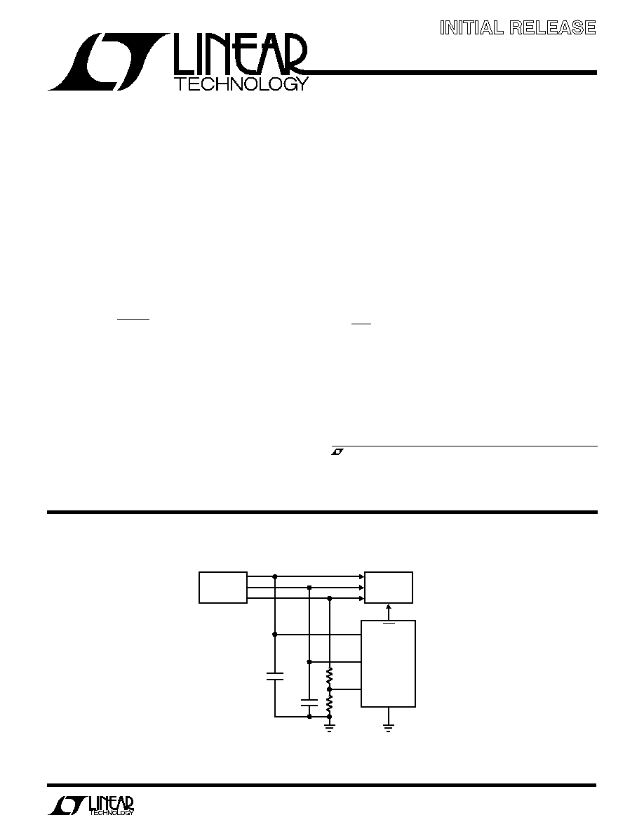
TYPICAL APPLICATIO
U
V
CC3
V
CC18
V
CCA
RST
LTC1985-1.8
GND
1985-1.8 TA01
3V
1.8V
2.5V
0.1
µ
F
5
1
2
R1
130k
1%
R2
100k
1%
4
3
DC/DC
CONVERTER
SYSTEM
LOGIC
0.1
µ
F
Information furnished by Linear Technology Corporation is believed to be accurate and reliable.
However, no responsibility is assumed for its use. Linear Technology Corporation makes no represen-
tation that the interconnection of its circuits as described herein will not infringe on existing patent rights.
2
LTC1985-1.8
(Notes 1, 2)
V
CC3
, V
CC18
, V
CCA
...................................... ≠ 0.3V to 7V
RST .......................................... ≠ 0.3V to (V
CC3
+ 0.3V)
Operating Temperature Range
(Note 3) ............................................. ≠ 40
∞
C to 85
∞
C
Storage Temperature Range ................ ≠ 65
∞
C to 150
∞
C
Lead Temperature (Soldering, 10 sec)................ 300
∞
C
Consult factory for Industrial and Military grade parts.
T
JMAX
= 125
∞
C,
JA
= 250
∞
C/W
RST 1
GND 2
TOP VIEW
S5 PACKAGE
5-LEAD PLASTIC SOT-23
V
CCA
3
5 V
CC3
4 V
CC18
SYMBOL
PARAMETER
CONDITIONS
MIN
TYP
MAX
UNITS
V
RT3
Reset Threshold V
CC3
V
CC3
Input Threshold
q
2.760
2.805
2.850
V
V
RT18
Reset Threshold V
CC18
V
CC18
Input Threshold
q
1.656
1.683
1.710
V
V
RTA
Reset Threshold V
CCA
V
CCA
Input Threshold
q
0.985
1.000
1.015
V
V
CCOP
V
CC3
, V
CC18
Operating Voltage
RST in Correct Logic State
q
1
7
V
I
VCC3
V
CC3
Supply Current
V
CC18
> V
CC3
q
1
2
µ
A
V
CC18
< V
CC3
, V
CC3
= 3V (Note 4)
q
10
20
µ
A
I
VCC18
V
CC18
Supply Current
V
CC18
< V
CC3
, V
CC18
= 1.8V (Note 4)
q
1
2
µ
A
I
VCCA
V
CCA
Input Current
V
CCA
= 1V
q
≠ 15
0
15
nA
t
RST
Reset Pulse Width
RST Low
q
140
200
280
ms
t
UV
V
CC
Undervoltage Detect to RST
V
CC18
, V
CC3
or V
CCA
Less Than Reset
110
µ
s
Threshold V
RT
by More Than 1%
V
OL
Output Voltage Low, RST
I
SINK
= 2.5mA, V
CC3
= 3V, V
CC18
= 0V
q
0.15
0.4
V
I
SINK
= 100
µ
A, V
CC3
= 1V, V
CC18
= 0V
q
0.05
0.3
V
I
SINK
= 100
µ
A, V
CC3
= 0V, V
CC18
= 1V
q
0.05
0.3
V
I
SINK
= 100
µ
A, V
CC3
= 1V, V
CC18
= 1V
q
0.05
0.3
V
V
OH
Output Voltage High, RST
I
SOURCE
= 200
µ
A
q
0.8V
CC3
V
The
q
denotes specifications which apply over the full operating
temperature range, otherwise specificaitons are at T
A
= 25
∞
C. V
CC3
= 3V, V
CC18
= 1.8V, V
CCA
= V
CC3
unless otherwise noted.
ORDER
PART NUMBER
LTC1985ES5-1.8
S5 PART MARKING
ELECTRICAL CHARACTERISTICS
ABSOLUTE AXI U RATI GS
W
W
W
U
PACKAGE/ORDER I FOR ATIO
U
U
W
LTNM
Note 1: Absolute Maximum Ratings are those values beyond which the life
of the device may be impaired.
Note 2: All voltage values are with respect to GND.
Note 3: The LTC1985E is guaranteed to meet specified performance from
0
∞
C to 70
∞
C and is designed, characterized and assured to meet the
extended temperature limits of ≠ 40
∞
C to 85
∞
C but are not tested at these
temperatures.
Note 4: Both V
CC3
and V
CC18
can act as the supply depending on which pin
has the greatest potential.
3
LTC1985-1.8
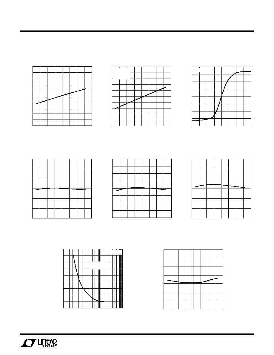
TYPICAL PERFOR A CE CHARACTERISTICS
U
W
I
VCC18
vs Temperature
V
CCA
Input Current
vs Input Voltage
TEMPERATURE (
∞
C)
≠ 60
0.5
I
VCC18
(
µ
A)
0.6
0.8
0.9
1.0
1.5
1.2
≠ 20
20
40
1985-18 G02
0.7
1.3
1.4
1.1
≠40
0
60
80
100
V
CC3
= 3V
V
CCA
= 3V
V
CC18
= 1.8V
INPUT VOLTAGE (V)
0.80 0.85
0.95
1.05
1.15
INPUT CURRENT (nA)
0
1.0
1.20
1985-18 G03
≠1.0
≠ 2.0
≠ 0.5
≠1.5
0.90
1
1.10
2.0
0.5
1.5
T
A
= 25
∞
C
V
CCA
Threshold Voltage
vs Temperature
Reset Pulse Width
vs Temperature
Typical Transient Duration
vs Comparator Overdrive
V
CC3
Threshold Voltage
vs Temperature
I
VCC3
vs Temperature
TEMPERATURE (
∞
C)
≠60
0.985
V
CCA
THRESHOLD VOLTAGE, V
RTA
(V)
0.990
0.995
1.000
1.005
≠20
20
60
100
1985-18 G04
1.010
1.015
≠40
0
40
80
TEMPERATURE (
∞
C)
≠ 60
V
CC3
THRESHOLD VOLTAGE, V
RT3
(V)
≠ 20
20
40
1985-18 G05
2.845
2.835
2.825
2.815
2.805
2.795
2.785
2.775
2.765
≠40
0
60
80
100
RESET COMPARATOR OVERDRIVE VOLTAGE (% OF V
CC
)
0.1
250
TYPICAL TRANSIENT DIRATION (
µ
s)
300
350
400
450
1
10
100
1985-18 G07
200
150
50
0
100
RESET OCCURS
ABOVE CURVE
T
A
= 25
∞
C
TEMPERATURE (
∞
C)
≠60 ≠40
RESET PULSE WIDTH, t
RST
(ms)
220
240
260
60
1985-18 G08
200
180
≠20
20
40
80
0
100
160
140
280
TEMPERATURE (
∞
C)
≠ 60
5
I
VCC3
(
µ
A)
6
8
9
10
15
12
≠ 20
20
40
1985-18 G01
7
13
14
11
≠40
0
60
80
100
V
CC18
Threshold Voltage
vs Temperature
TEMPERATURE (
∞
C)
≠60
1.650
V
CC18
THRESHOLD VOLTAGE, V
RT18
(V)
1.660
1.670
1.680
1.690
≠20
20
60
100
1985-18 G06
1.700
1.710
≠40
0
40
80

4
LTC1985-1.8
RST (Pin 1): Reset Logic Output. Active low, 3V push-
pull output. Asserted when one or all of the supplies are
below trip thresholds and held for 200ms after all sup-
plies become valid.
GND (Pin 2): Ground.
V
CCA
(Pin 3): 1V Sense, High Impedance Input. If unused
it can be tied to either V
CC3
or V
CC18
.
U
U
U
PI FU CTIO S
V
CC18
(Pin 4): 1.8V Sense Input and Power Supply Pin.
This pin is used on the LTC1985 to provide power to the
part when the voltage on V
CC18
is greater than the voltage
on V
CC3
. Bypass to ground with a
0.1
µ
F ceramic
capacitor.
V
CC3
(Pin 5): 3V Sense Input and Power Supply Pin. This
pin provides power to the part when the voltage on V
CC3
is greater than the voltage on V
CC18
. Bypass to ground
with a
0.1
µ
F ceramic capacitor.
200ms
DELAY
V
CC
INTERNAL
BANDGAP
REFERENCE
POWER
DETECT
200ms PULSE GENERATOR
≠
+
≠
+
≠
+
5
V
CC3
4
V
CC18
3
V
CCA
2
GND
1985-18 BD
1
RST
LTC1985-1.8
V
CC3
BLOCK DIAGRA
W
5
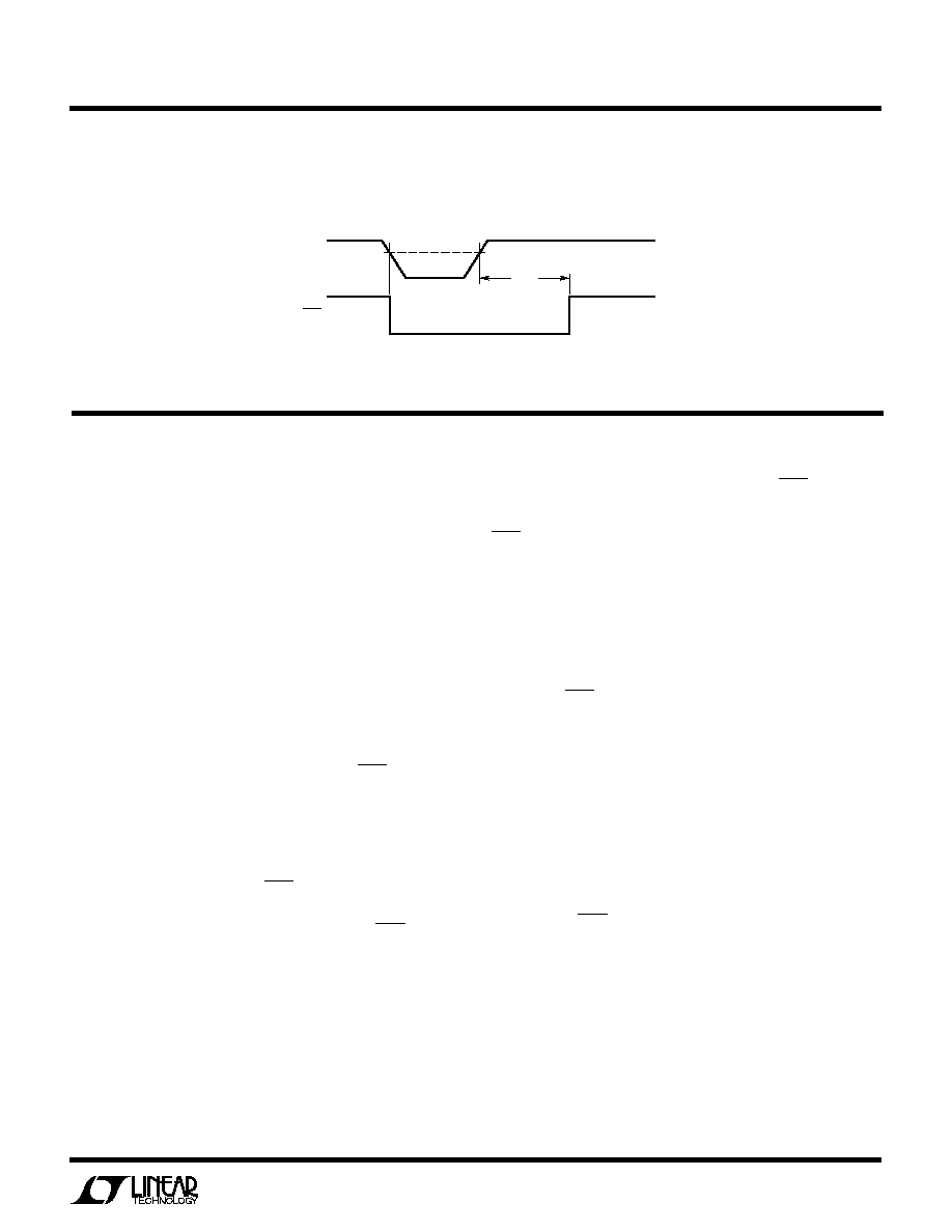
LTC1985-1.8
V
CC
Monitor Timing
t
RST
1985-18 TD
V
RTX
V
CCX
RST
TI I G DIAGRA
U
W
W
Supply Monitoring
The LTC1985 is a low power, high accuracy triple supply
monitoring cirucit with a single 200ms microprocessor
reset output.
All three V
CC
inputs must be above predetermined thresh-
olds for reset not to be invoked. The LTC1985 will assert
reset during power-up, power-down and brownout condi-
tions on any one or all of the V
CC
inputs.
3V or 1.8V Power Detect
The LTC1985 is powered from the 3V input pin (V
CC3
) or
the 1.8V input pin (V
CC18
), whichever pin has the highest
potential. This ensures the part pulls the RST pin low as
soon as either input pin is
1V.
Power-Up
Upon power-up, either the V
CC18
or V
CC3
pin, can power
the part. This ensures that RST will be low when either
V
CC18
or V
CC3
reaches 1V. As long as any one of the V
CC
inputs is below its predetermined threshold, RST will stay
a logic low. Once all of the V
CC
inputs rise above their
thresholds, an internal timer is started and RST is released
after 200ms.
RST is reasserted whenever any one of the V
CC
inputs
drops below its predetermined threshold and remains
asserted until 200ms after all of the V
CC
inputs are above
their thresholds.
Power-Down
On power-down, once any of the V
CC
inputs drop below its
threshold, RST is held at a logic low. A logic low of 0.3V is
guaranteed until both V
CC3
and V
CC18
drop below 1V.
Override Functions
The V
CCA
pin, if unused, can be tied to either V
CC3
or V
CC18
.
This is an obvious solution since the trip points for V
CC3
and V
CC18
will always be greater than the trip point for
V
CCA
. Likewise, the V
CC18
, if unused, can be tied to V
CC3
.
V
CC3
must always be used. Tying V
CC3
to V
CC18
and
operating off of a 1.8V supply will result in the continuous
assertion of RST.
APPLICATIO S I FOR ATIO
W
U
U
U