 | ÐлекÑÑоннÑй компоненÑ: LTC3405A | СкаÑаÑÑ:  PDF PDF  ZIP ZIP |
3405af.pm6
1
LTC3405A
sn3405af 3405afs
s
High Efficiency: Up to 96%
s
Very Low Quiescent Current: Only 20
µ
A
During Operation
s
300mA Output Current at V
IN
= 3V
s
2.5V to 5.5V Input Voltage Range
s
1.5MHz Constant Frequency Operation
s
No Schottky Diode Required
s
Low Dropout Operation: 100% Duty Cycle
s
Stable with Ceramic Capacitors
s
0.8V Reference Allows Low Output Voltages
s
Shutdown Mode Draws < 1
µ
A Supply Current
s
±
2% Output Voltage Accuracy
s
Current Mode Operation for Excellent Line and
Load Transient Response
s
Overtemperature Protected
s
Low Profile (1mm) ThinSOT
TM
Package
The LTC
®
3405A is a high efficiency monolithic synchro-
nous buck regulator using a constant frequency, current
mode architecture. Supply current during operation is
only 20
µ
A and drops to <1
µ
A in shutdown. The 2.5V to
5.5V input voltage range makes the LTC3405A ideally
suited for single Li-Ion battery-powered applications. 100%
duty cycle provides low dropout operation, extending
battery life in portable systems.
Switching frequency is internally set at 1.5MHz, allowing
the use of small surface mount inductors and capacitors.
The LTC3405A is specifically designed to work well with
ceramic output capacitors, achieving very low output
voltage ripple and a small PCB footprint.
The internal synchronous switch increases efficiency and
eliminates the need for an external Schottky diode. Low
output voltages are easily supported with the 0.8V feed-
back reference voltage. The LTC3405A is available in a low
profile (1mm) ThinSOT package.
For fixed 1.5V and 1.8V output versions, refer to the
LTC3405A-1.5/LTC3405A-1.8 data sheet.
s
Cellular Telephones
s
Personal Information Appliances
s
Wireless and DSL Modems
s
Digital Still Cameras
s
MP3 Players
s
Portable Instruments
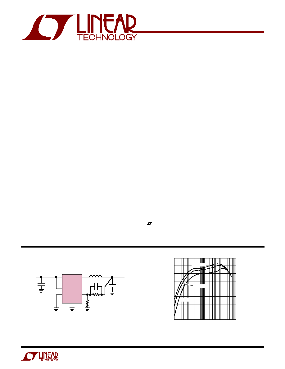
Figure 1a. High Efficiency Step-Down Converter
1.5MHz, 300mA
Synchronous Step-Down
Regulator in ThinSOT
Figure 1b. Efficiency vs Load Current
V
IN
C
IN
2.2
µ
F
CER
V
IN
2.7V
TO 5.5V
*
**
LTC3405A
RUN
MODE
3
4.7
µ
H**
22pF
887k
280k
3405A F01a
V
OUT
CONNECTED TO V
IN
FOR 2.7V < V
IN
< 3.3V
MURATA LQH3C4R7M34
TAIYO YUDEN LMK212BJ225MG
TAIYO YUDEN JMK212BJ475MG
5
4
6
1
2
SW
V
FB
GND
C
OUT
4.7
µ
F
CER
V
OUT
*
3.3V
, LTC and LT are registered trademarks of Linear Technology Corporation.
ThinSOT is a trademark of Linear Technology Corporation.
OUTPUT CURRENT (mA)
0.1
EFFICIENCY (%)
10
1000
100
95
90
85
80
75
70
65
60
3405A F01b
1
100
V
IN
= 3.6V
V
IN
= 4.2V
V
IN
= 5.5V
APPLICATIO S
U
FEATURES
TYPICAL APPLICATIO
U
DESCRIPTIO
U
2
LTC3405A
sn3405af 3405afs
SYMBOL
PARAMETER
CONDITIONS
MIN
TYP
MAX
UNITS
I
VFB
Feedback Current
q
±
30
nA
I
PK
Peak Inductor Current
V
IN
= 3V, V
FB
= 0.7V, Duty Cycle < 35%
375
500
625
mA
V
FB
Regulated Feedback Voltage
(Note 4)
q
0.784
0.8
0.816
V
V
OVL
Output Overvoltage Lockout
V
OVL
= V
OVL
V
FB
q
20
50
80
mV
V
FB
Reference Voltage Line Regulation
V
IN
= 2.5V to 5.5V (Note 4)
q
0.04
0.4
%/V
V
LOADREG
Output Voltage Load Regulation
0.5
%
V
IN
Input Voltage Range
q
2.5
5.5
V
I
S
Input DC Bias Current
(Note 5)
Pulse Skipping Mode
V
FB
= 0.7V, Mode = 3.6V, I
LOAD
= 0A
300
400
µ
A
Burst Mode
®
Operation
V
FB
= 0.83V, Mode = 0V, I
LOAD
= 0A
20
35
µ
A
Shutdown
V
RUN
= 0V, V
IN
= 4.2V
0.1
1
µ
A
f
OSC
Oscillator Frequency
V
FB
= 0.8V
q
1.2
1.5
1.8
MHz
V
FB
= 0V
210
kHz
R
PFET
R
DS(ON)
of P-Channel FET
I
SW
= 100mA
0.7
0.85
R
NFET
R
DS(ON)
of N-Channel FET
I
SW
= 100mA
0.6
0.90
I
LSW
SW Leakage
V
RUN
= 0V, V
SW
= 0V or 5V, V
IN
= 5V
±
0.01
±
1
µ
A
V
RUN
RUN Threshold
q
0.3
1
1.5
V
I
RUN
RUN Leakage Current
q
±
0.01
±
1
µ
A
V
MODE
MODE Threshold
q
0.3
1.5
2
V
I
MODE
MODE Leakage Current
q
±
0.01
±
1
µ
A
Burst Mode is a registered trademark of Linear Technology Corporation.
LTC3405AES6
T
JMAX
= 125
°
C,
JA
= 250
°
C/ W
ORDER PART
NUMBER
(Note 1)
Input Supply Voltage .................................. 0.3V to 6V
MODE, RUN, V
FB
Voltages ......................... 0.3V to V
IN
SW Voltage .................................. 0.3V to (V
IN
+ 0.3V)
P-Channel Switch Source Current (DC) ............. 400mA
N-Channel Switch Sink Current (DC) ................. 400mA
Peak SW Sink and Source Current .................... 630mA
Operating Temperature Range (Note 2) .. 40
°
C to 85
°
C
Junction Temperature (Note 3) ............................ 125
°
C
Storage Temperature Range ................ 65
°
C to 150
°
C
Lead Temperature (Soldering, 10 sec)................. 300
°
C
S6 PART MARKING
Consult LTC Marketing for parts specified with wider operating temperature ranges.
The
q
denotes specifications which apply over the full operating temperature range, otherwise specifications are T
A
= 25
°
C.
V
IN
= 3.6V unless otherwise specified.
LTZW
ABSOLUTE AXI U RATI GS
W
W
W
U
PACKAGE/ORDER I FOR ATIO
U
U
W
ELECTRICAL CHARACTERISTICS
RUN 1
GND 2
SW 3
6 MODE
5 V
FB
4 V
IN
TOP VIEW
S6 PACKAGE
6-LEAD PLASTIC SOT-23
Note 1: Absolute Maximum Ratings are those values beyond which the life
of a device may be impaired.
Note 2: The LTC3405AE is guaranteed to meet performance specifications
from 0
°
C to 70
°
C. Specifications over the 40
°
C to 85
°
C operating
temperature range are assured by design, characterization and correlation
with statistical process controls.
Note 3: T
J
is calculated from the ambient temperature T
A
and power
dissipation P
D
according to the following formula:
LTC3405A: T
J
= T
A
+ (P
D
)(250
°
C/W)
Note 4: The LTC3405A is tested in a proprietary test mode that connects
V
FB
to the output of the error amplifier.
Note 5: Dynamic supply current is higher due to the gate charge being
delivered at the switching frequency.
3
LTC3405A
sn3405af 3405afs
INPUT VOLTAGE (V)
2.5
3.0
4.0
5.0
EFFICIENCY (%)
4.5
95
90
85
80
75
70
65
60
55
50
3405A G02
3.5
5.5
Burst Mode OPERATION
V
OUT
= 1.8V
I
OUT
= 0.1mA
I
OUT
= 250mA
I
OUT
= 100mA
I
OUT
= 10mA
I
OUT
= 1mA
OUTPUT CURRENT (mA)
0.1
EFFICIENCY (%)
10
1000
100
90
80
70
60
50
40
30
20
10
0
3405A G03
1
100
V
IN
= 3.6V
V
IN
= 4.2V
V
IN
= 3.6V
V
IN
= 4.2V
V
OUT
= 1.8V
PULSE SKIPPING MODE
Burst Mode OPERATION
OUTPUT CURRENT (mA)
0.1
EFFICIENCY (%)
10
1000
100
90
80
70
60
50
40
3405A G04
1
100
V
IN
= 2.7V
V
IN
= 5.5V
V
IN
= 4.2V
V
IN
= 3.6V
V
OUT
= 1.8V
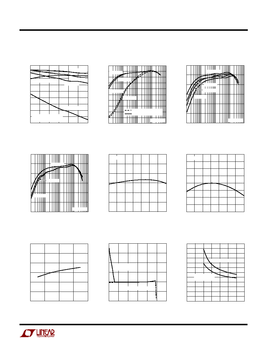
TYPICAL PERFOR A CE CHARACTERISTICS
U
W
OUTPUT CURRENT (mA)
0.1
EFFICIENCY (%)
10
1000
100
90
80
70
60
50
40
3405A G05
1
100
V
IN
= 2.7V
V
IN
= 4.2V
V
OUT
= 1.3V
V
IN
= 3.6V
Efficiency vs Input Voltage
Efficiency vs Output Current
Efficiency vs Output Current
Efficiency vs Output Current
Reference Voltage vs
Temperature
Oscillator Frequency vs
Temperature
Oscillator Frequency vs
Supply Voltage
Output Voltage vs Load Current
R
DS(ON
) vs Input Voltage
TEMPERATURE (
°
C)
50
REFERENCE VOLTAGE (V)
0.814
0.809
0.804
0.799
0.794
0.789
0.784
25
75
25
0
50
100
125
V
IN
= 3.6V
3405A G06
TEMPERATURE (
°
C)
50
FREQUENCY (MHz)
1.70
1.65
1.60
1.55
1.50
1.45
1.40
1.35
1.30
25
75
25
0
50
100
125
V
IN
= 3.6V
3405A G07
SUPPLY VOLTAGE (V)
2
OSCILLATOR FREQUENCY (MHz)
1.8
1.7
1.6
1.5
1.4
1.3
1.2
3
4
5
6
3405A G08
LOAD CURRENT (mA)
0
OUTPUT VOLTAGE (V)
1.834
1.824
1.814
1.804
1.794
1.784
1.774
100
200
300
400
3405A
G09
500
600
Burst Mode
OPERATION
PULSE SKIPPING MODE
INPUT VOLTAGE (V)
0
R
DS(0N)
(
)
2
4
5
3405A G10
1
3
6
7
1.2
1.1
1.0
0.9
0.8
0.7
0.6
0.5
0.4
0.3
0.2
0.1
0
MAIN SWITCH
SYNCHRONOUS
SWITCH
(From Figure1a Except for the Resistive Divider Resistor Values)
4
LTC3405A
sn3405af 3405afs
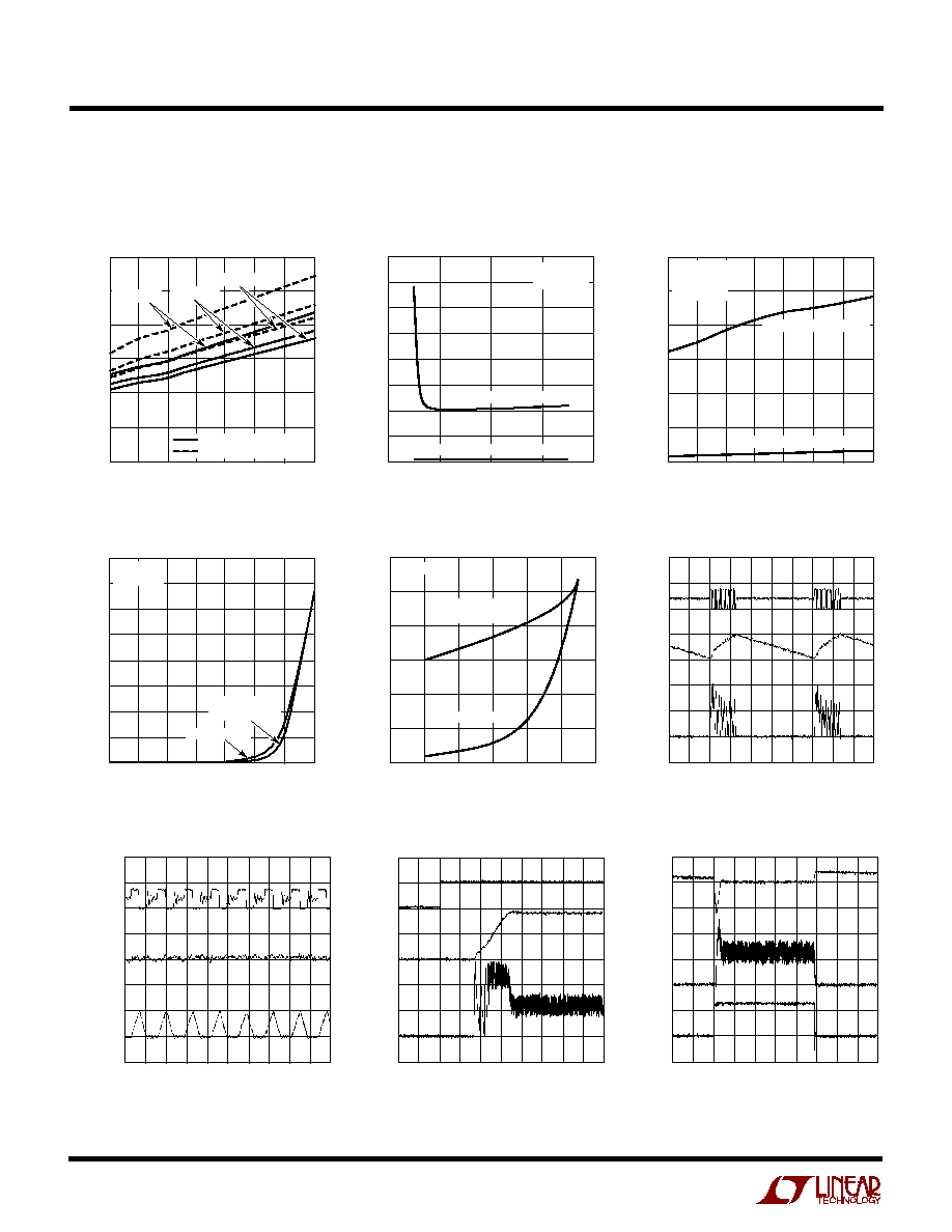
R
DS(ON)
vs Temperature
Dynamic Supply Current
Dynamic Supply Current
vs Temperature
Switch Leakage vs Temperature
Switch Leakage vs Input Voltage
TEMPERATURE (
°
C)
50
R
DS(ON)
(
)
1.2
1.0
0.8
0.6
0.4
0.2
0
25
75
25
0
50
100
125
3405A G11
SYNCHRONOUS SWITCH
MAIN SWITCH
V
IN
= 2.7V
V
IN
= 3.6V
V
IN
= 4.2V
SUPPLY VOLTAGE (V)
2
DYNAMIC SUPPLY CURRENT (
µ
A)
1600
1400
1200
1000
800
600
400
200
0
3
4
5
6
3405A G12
V
OUT
= 1.8V
I
LOAD
= 0A
PULSE SKIPPING MODE
Burst Mode OPERATION
TEMPERATURE (
°
C)
50
DYNAMIC SUPPLY CURRENT (
µ
A)
600
500
400
300
200
100
0
25
75
25
0
50
100
125
V
IN
= 3.6V
V
OUT
= 1.8V
I
LOAD
= 0A
3405A G13
PULSE SKIPPING MODE
Burst Mode OPERATION
TEMPERATURE (
°
C)
50
SWITCH LEAKAGE (nA)
160
140
120
100
80
60
40
20
0
25
75
25
0
50
100
125
V
IN
= 5.5V
RUN = 0V
3405A G14
MAIN SWITCH
SYNCHRONOUS
SWITCH
INPUT VOLTAGE (V)
0
SWITCH LEAKAGE (pA)
60
50
40
30
20
10
0
1
2
3
4
3405A G15
5
6
RUN = 0V
MAIN SWITCH
SYNCHRONOUS
SWITCH
SW
5V/DIV
V
OUT
100mV/DIV
AC COUPLED
I
L
100mA/DIV
3405A
G16
5
µ
s/DIV
V
IN
= 3.6V
V
OUT
= 1.8V
I
LOAD =
20mA
SW
5V/DIV
V
OUT
10mV/DIV
AC
COUPLED
I
L
100mA/DIV
3405A
G17
500ns/DIV
V
IN
= 3.6V
V
OUT
= 1.8V
I
LOAD =
20mA
RUN
2V/DIV
V
OUT
1V/DIV
I
L
200mA/DIV
3405A
G18
100
µ
s/DIV
V
IN
= 3.6V
V
OUT
= 1.8V
I
LOAD =
250mA
3405A
G19
V
OUT
100mV/DIV
AC
COUPLED
I
LOAD
200mA/DIV
I
L
200mA/DIV
40
µ
s/DIV
V
IN
= 3.6V
V
OUT
= 1.8V
I
LOAD =
0mA TO 250mA
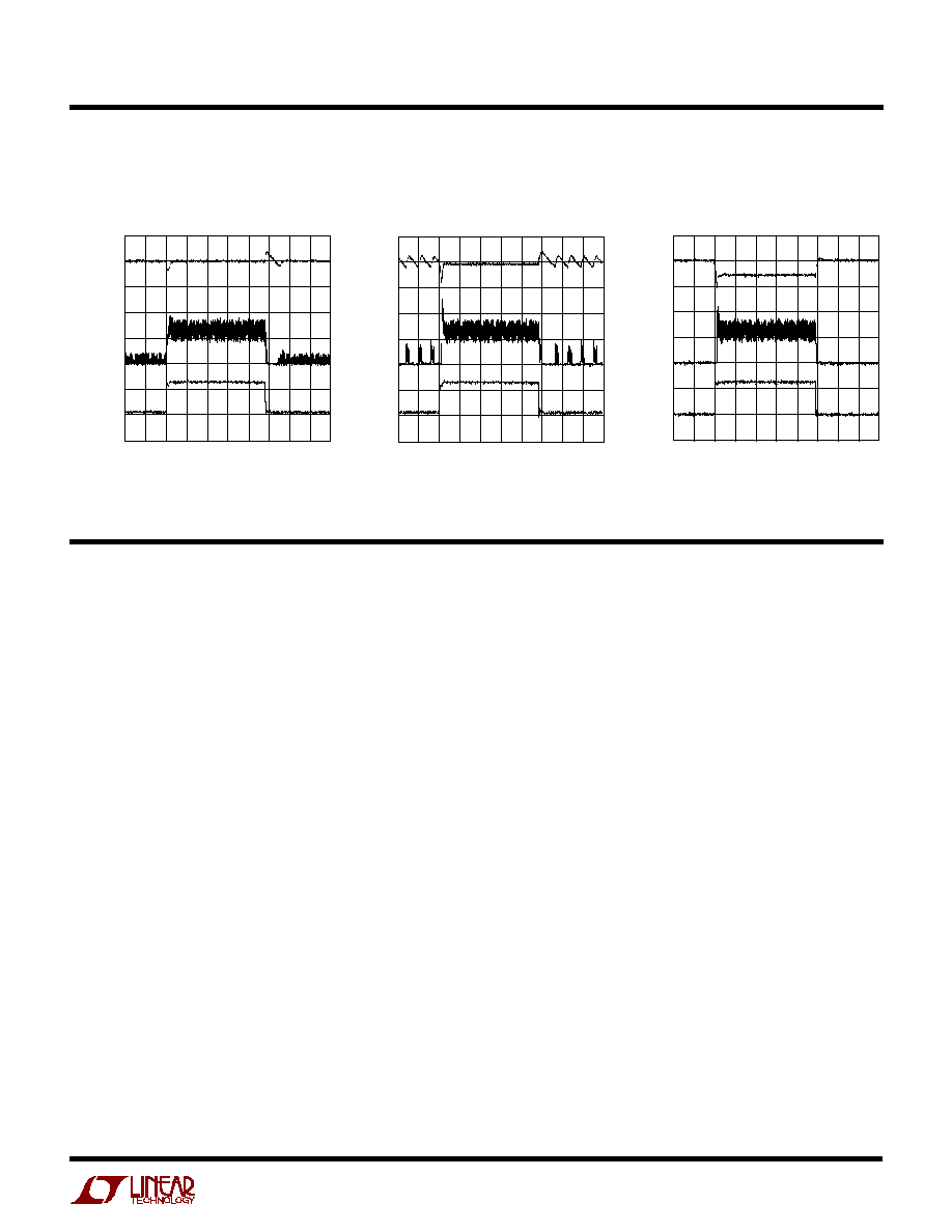
PULSE SKIPPING MODE
TYPICAL PERFOR A CE CHARACTERISTICS
U
W
(From Figure 1a Except for the Resistive Divider Resistor Values)
Burst Mode Operation
Pulse Skipping Mode Operation
Start-Up from Shutdown
Load Step
5
LTC3405A
sn3405af 3405afs
U
U
U
PI FU CTIO S
RUN (Pin 1): Run Control Input. Forcing this pin above
1.5V enables the part. Forcing this pin below 0.3V shuts
down the device. In shutdown, all functions are disabled
drawing <1
µ
A supply current. Do not leave RUN floating.
GND (Pin 2): Ground Pin.
SW (Pin 3): Switch Node Connection to Inductor. This pin
connects to the drains of the internal main and synchro-
nous power MOSFET switches.
V
IN
(Pin 4): Main Supply Pin. Must be closely decoupled
to GND, Pin 2, with a 2.2
µ
F or greater ceramic capacitor.
V
FB
(Pin 5): Feedback Pin. Receives the feedback voltage
from an external resistive divider across the output.
MODE (Pin 6): Mode Select Input. To select pulse skip-
ping mode, tie to V
IN
. Grounding this pin selects Burst
Mode operation. Do not leave this pin floating.
3405A
G20
V
OUT
100mV/DIV
AC
COUPLED
I
LOAD
200mA/DIV
I
L
200mA/DIV
40
µ
s/DIV
V
IN
= 3.6V
V
OUT
= 1.8V
I
LOAD =
20mA TO 250mA
PULSE SKIPPING MODE
V
OUT
100mV/DIV
AC
COUPLED
I
LOAD
200mA/DIV
I
L
200mA/DIV
3405A
G21
40
µ
s/DIV
V
IN
= 3.6V
V
OUT
= 1.8V
I
LOAD =
20mA TO 250mA
Burst Mode OPERATION
3405A
G22
40
µ
s/DIV
V
IN
= 3.6V
V
OUT
= 1.8V
I
LOAD =
0mA TO 250mA
Burst Mode OPERATION
V
OUT
100mV/DIV
AC
COUPLED
I
LOAD
200mA/DIV
I
L
200mA/DIV
TYPICAL PERFOR A CE CHARACTERISTICS
U
W
Load Step
Load Step
Load Step
(From Figure 1a Except for the Resistive Divider Resistor Values)