Äîêóìåíòàöèÿ è îïèñàíèÿ www.docs.chipfind.ru
1
LTC3406B-1.2
sn3406b12 3406b12fs
, LTC and LT are registered trademarks of Linear Technology Corporation. All other
trademarks are the property of their respective owners. ThinSOT is a trademark of Linear
Technology Corporation. Protected by U.S. Patents including 5481178, 6580258, 6304066,
6127815, 6498466, 6611131.
High Efficiency: Up to 96%
600mA Output Current at V
IN
= 3V
2.5V to 5.5V Input Voltage Range
1.5MHz Constant Frequency Operation
No Schottky Diode Required
Low Quiescent Current: 300µA
Shutdown Mode Draws < 1µA Supply Current
Current Mode Operation for Excellent Line and
Load Transient Response
Overtemperature Protected
Low Profile (1mm) ThinSOT
TM
Package
The LTC
®
3406B-1.2 is a high efficiency monolithic syn-
chronous buck regulator using a constant frequency,
current mode architecture. Supply current with no load is
300µA dropping to <1µA in shutdown. The 2.5V to 5.5V
input voltage range makes the LTC3406B-1.2 ideally suited
for single Li-Ion battery-powered applications. 100% duty
cycle provides low dropout operation, extending battery
life in portable systems. PWM pulse skipping mode opera-
tion provides very low output ripple voltage for noise
sensitive applications.
Switching frequency is internally set at 1.5MHz, allowing
the use of small surface mount inductors and capacitors.
The internal synchronous switch increases efficiency and
eliminates the need for an external Schottky diode. The
LTC3406B-1.2 is available in a low profile (1mm) ThinSOT
package.
Cellular Telephones
Personal Information Appliances
Wireless and DSL Modems
Digital Still Cameras
MP3 Players
Portable Instruments
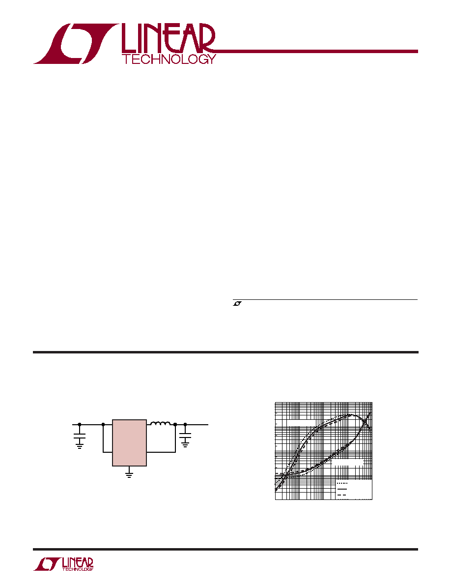
High Efficiency Step-Down Converter
1.5MHz, 600mA
Synchronous Step-Down
Regulator in ThinSOT
Efficiency and Power Loss
FEATURES
DESCRIPTIO
U
APPLICATIO S
U
TYPICAL APPLICATIO
U
V
IN
C
IN
4.7µF
CER
V
IN
2.7V TO 5.5V
LTC3406B-1.2
RUN
2.2µH
3406B12 TA01a
SW
V
OUT
GND
C
OUT
10µF
CER
V
OUT
1.2V
600mA
LOAD CURRENT (mA)
0.1
10
1000
100
90
80
70
60
50
40
30
20
10
3406B12 TA01b
1
100
1
0.1
0.01
0.001
0.0001
V
IN
= 2.7V
V
IN
= 3.6V
V
IN
= 4.2V
EFFICIENCY
POWER LOSS
POWER LOSS (W)
EFFICIENCY (%)
2
LTC3406B-1.2
sn3406b12 3406b12fs
SYMBOL
PARAMETER
CONDITIONS
MIN
TYP
MAX
UNITS
V
OUT
Regulated Output Voltage
1.164
1.2
1.236
V
V
OVL
Output Overvoltage Lockout
V
OVL
= V
OVL
V
OUT
2.5
6.25
10
%
V
OUT
Output Voltage Line Regulation
V
IN
= 2.5V to 5.5V
0.04
0.4
%/V
I
PK
Peak Inductor Current
V
IN
= 3V, V
OUT
= 1.08V, Duty Cycle < 35%
0.75
1
1.25
A
V
LOADREG
Output Voltage Load Regulation
0.5
%
V
IN
Input Voltage Range
2.5
5.5
V
I
S
Input DC Bias Current
(Note 4)
V
OUT
= 1.08V
300
400
µA
Shutdown
V
RUN
= 0V, V
IN
= 5.5V
0.1
1
µA
f
OSC
Oscillator Frequency
V
OUT
= 1.2V
1.2
1.5
1.8
MHz
V
OUT
= 0V
210
kHz
R
PFET
R
DS(ON)
of P-Channel FET
I
SW
= 100mA
0.4
0.5
R
NFET
R
DS(ON)
of N-Channel FET
I
SW
= 100mA
0.35
0.45
I
LSW
SW Leakage
V
RUN
= 0V, V
SW
= 0V or 5V, V
IN
= 5V
±0.01
±1
µA
V
RUN
RUN Threshold
0.3
1
1.5
V
I
RUN
RUN Leakage Current
±0.01
±1
µA
Input Supply Voltage .................................. 0.3V to 6V
RUN, V
OUT
Voltages................................... 0.3V to V
IN
SW Voltage (DC) ......................... 0.3V to (V
IN
+ 0.3V)
P-Channel Switch Source Current (DC) ............. 800mA
N-Channel Switch Sink Current (DC) ................. 800mA
Peak SW Sink and Source Current (V
IN
= 3V)........ 1.3A
Operating Temperature Range (Note 2) .. 40°C to 85°C
Junction Temperature (Notes 3, 5) ...................... 125°C
Storage Temperature Range ................ 65°C to 150°C
Lead Temperature (Soldering, 10 sec)................. 300°C
Consult LTC Marketing for parts specified with wider operating temperature ranges.
ABSOLUTE AXI U RATI GS
W
W
W
U
PACKAGE/ORDER I FOR ATIO
U
U
W
(Note 1)
LTC3406BES5-1.2
ORDER PART
NUMBER
S5 PART MARKING
LTBMR
T
JMAX
= 125°C,
JA
= 250°C/ W,
JC
= 90°C/ W
RUN 1
GND 2
TOP VIEW
S5 PACKAGE
5-LEAD PLASTIC TSOT-23
SW 3
5 V
OUT
4 V
IN
The
denotes specifications which apply over the full operating
temperature range, otherwise specifications are T
A
= 25°C. V
IN
= 3.6V unless otherwise specified.
ELECTRICAL CHARACTERISTICS
3
LTC3406B-1.2
sn3406b12 3406b12fs
Note 1: Absolute Maximum Ratings are those values beyond which the life
of a device may be impaired.
Note 2: The LTC3406BE-1.2 is guaranteed to meet performance
specifications from 0°C to 70°C. Specifications over the 40°C to 85°C
operating temperature range are assured by design, characterization and
correlation with statistical process controls.
Note 3: T
J
is calculated from the ambient temperature T
A
and power
dissipation P
D
according to the following formula:
LTC3406B-1.2: T
J
= T
A
+ (P
D
)(250°C/W)
Note 4: Dynamic supply current is higher due to the gate charge being
delivered at the switching frequency.
Note 5: This IC includes overtemperature protection that is intended to
protect the device during momentary overload conditions. Junction
temperature will exceed 125°C when overtemperature protection is active.
Continuous operation above the specified maximum operating junction
temperature may impair device reliability.
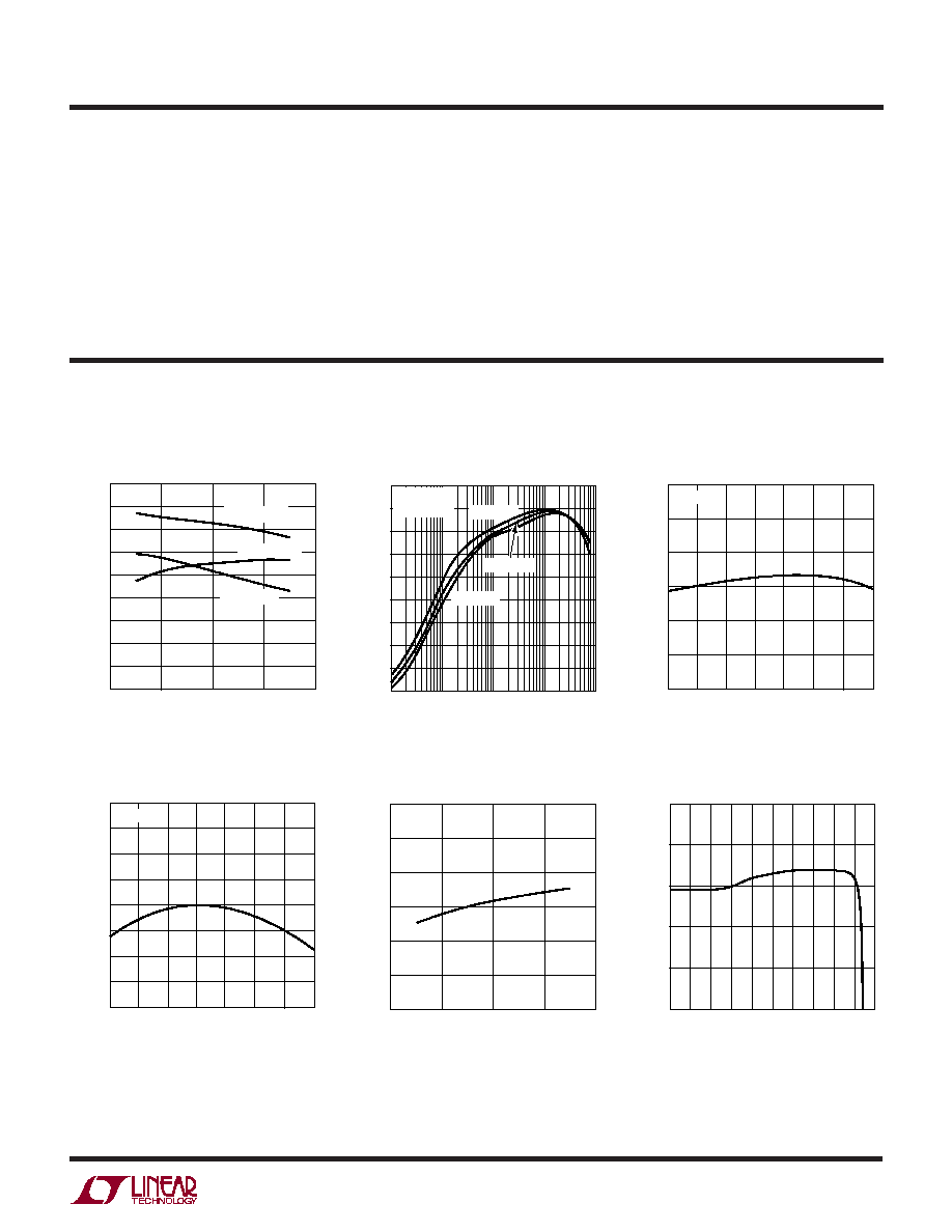
TYPICAL PERFOR A CE CHARACTERISTICS
U
W
Efficiency vs Input Voltage
Efficiency vs Output Current
Reference Voltage vs
Temperature
Oscillator Frequency vs
Temperature
(From Figure 1)
TEMPERATURE (°C)
50
REFERENCE VOLTAGE (V)
1.228
1.218
1.208
1.198
1.188
1.178
1.168
25
75
25
0
50
100
125
V
IN
= 3.6V
3406B12 G03
TEMPERATURE (°C)
50
FREQUENCY (MHz)
1.70
1.65
1.60
1.55
1.50
1.45
1.40
1.35
1.30
25
75
25
0
50
100
125
V
IN
= 3.6V
3406B12 G04
INPUT VOLTAGE (V)
2
EFFICIENCY (%)
6
3406B12 G01
3
4
5
95
90
85
80
75
70
65
60
55
50
I
OUT
= 600mA
I
OUT
= 100mA
I
OUT
= 10mA
OUTPUT CURRENT (mA)
0.1
EFFICIENCY (%)
10
1000
100
90
80
70
60
50
40
30
20
10
3406B12 GO2
1
100
V
OUT
= 1.2V
T
A
= 25°C
VIN = 2.7V
VIN = 4.2V
VIN = 3.6V
ELECTRICAL CHARACTERISTICS
LOAD CURRENT (mA)
0
OUTPUT VOLTAGE (V)
500
200 300 400
600
800
100
1.224
1.214
1.204
1.194
1.184
1.174
3406B12 G06
1000
900
700
Oscillator Frequency vs
Supply Voltage
Output Voltage vs Load Current
SUPPLY VOLTAGE (V)
2
OSCILLATOR FREQUENCY (MHz)
1.8
1.7
1.6
1.5
1.4
1.3
1.2
3
4
5
6
3406B12 G05
T
A
= 25°C
4
LTC3406B-1.2
sn3406b12 3406b12fs
TEMPERATURE (°C)
50
0.4
0.5
0.7
25
75
3406B12 G08
0.3
0.2
25
0
50
100
125
0.1
0
0.6
R
DS(ON)
(
)
MAIN SWITCH
SYNCHRONOUS SWITCH
V
IN
= 2.7V
V
IN
= 3.6V
V
IN
= 4.2V
TEMPERATURE (°C)
50
SWITCH LEAKAGE (nA)
200
250
300
25
75
3406B12 G11
150
100
25
0
50
100
125
50
0
V
IN
= 5.5V
RUN = 0V
MAIN SWITCH
SYNCHRONOUS SWITCH
INPUT VOLTAGE (V)
0
0
SWITCH LEAKAGE (pA)
20
40
60
80
120
1
2
3
4
3406B12 G12
5
6
100
RUN = 0V
T
A
= 25°C
SYNCHRONOUS
SWITCH
MAIN
SWITCH
SUPPLY VOLTAGE (V)
2
DYNAMIC SUPPLY CURRENT (
µ
A)
6
3406B12 G09
3
4
5
400
380
360
340
320
300
280
260
240
220
200
I
LOAD
= 0A
T
A
= 25°C
TEMPERATURE (°C)
50
340
320
300
280
260
240
220
200
25
75
3406B12 G10
25
0
50
100
125
DYNAMIC SUPPLY CURRENT (
µ
A)
V
IN
= 3.6V
I
LOAD
= 0A
SW
2V/DIV
V
OUT
10mV/DIV
AC COUPLED
I
L
200mA/DIV
1µs/DIV
V
IN
= 3.6V
I
LOAD
= 50mA
3406B12 G13
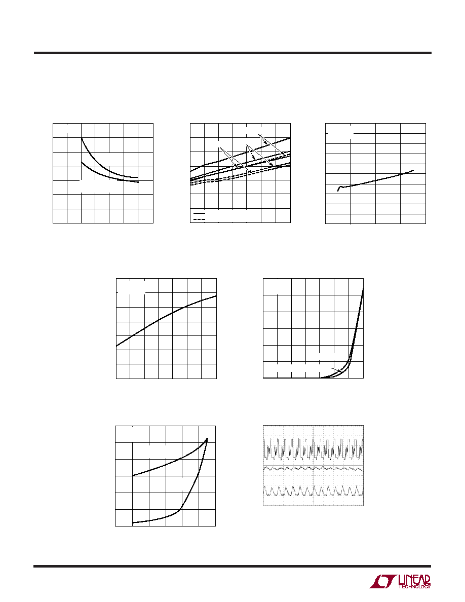
TYPICAL PERFOR A CE CHARACTERISTICS
U
W
R
DS(ON
) vs Input Voltage
(From Figure 1)
INPUT VOLTAGE (V)
1
0
0.4
0.5
0.7
4
6
3406B12 G07
0.3
0.2
2
3
5
7
0.1
0
0.6
R
DS(ON)
(
)
MAIN
SWITCH
SYNCHRONOUS
SWITCH
T
A
= 25°C
R
DS(ON)
vs Temperature
Dynamic Supply Current vs
Supply Voltage
Dynamic Supply Current vs
Temperature
Switch Leakage vs Temperature
Switch Leakage vs Input Voltage
Discontinuous Operation
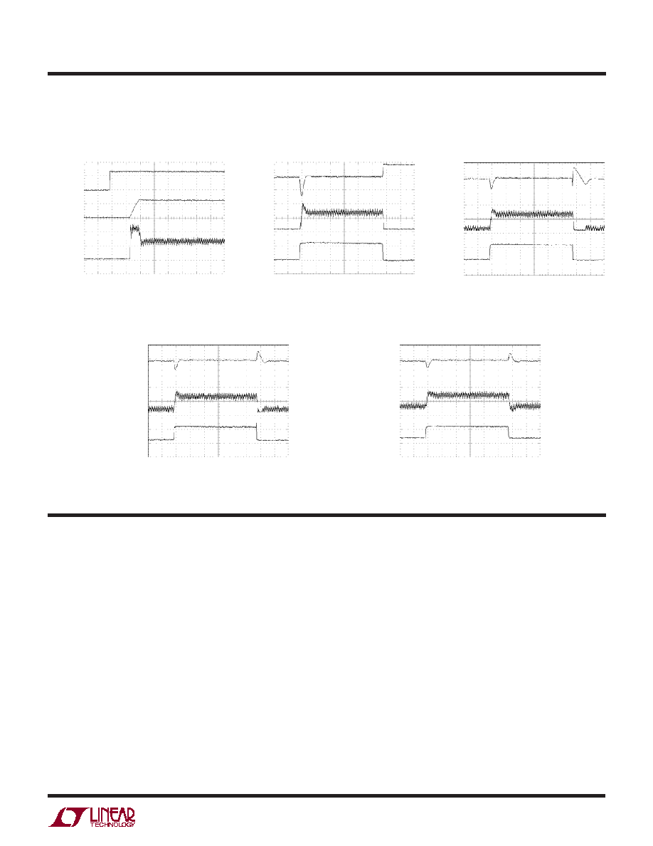
5
LTC3406B-1.2
sn3406b12 3406b12fs
TYPICAL PERFOR A CE CHARACTERISTICS
U
W
(From Figure 1a Except for the Resistive Divider Resistor Values)
Start-Up from Shutdown
Load Step
Load Step
Load Step
Load Step
U
U
U
PI FU CTIO S
RUN (Pin 1): Run Control Input. Forcing this pin above
1.5V enables the part. Forcing this pin below 0.3V shuts
down the device. In shutdown, all functions are disabled
drawing <1µA supply current. Do not leave RUN floating.
GND (Pin 2): Ground Pin.
SW (Pin 3): Switch Node Connection to Inductor. This pin
connects to the drains of the internal main and synchro-
nous power MOSFET switches.
V
IN
(Pin 4): Main Supply Pin. Must be closely decoupled
to GND, Pin 2, with a 2.2µF or greater ceramic capacitor.
V
OUT
(Pin 5): Output Voltage Feedback Pin. An internal
resistive divider divides the output voltage down for com-
parison to the internal reference voltage.
RUN
2V/DIV
V
OUT
1V/DIV
I
L
500mA/DIV
50µs/DIV
V
IN
= 3.6V
I
LOAD
= 600mA
3406B12 G14
V
OUT
100mV/DIV
AC COUPLED
I
L
500mA/DIV
I
LOAD
500mA/DIV
25µs/DIV
V
IN
= 3.6V
I
LOAD
= 0mA TO 600mA
3406B12 G15
V
OUT
100mV/DIV
AC COUPLED
I
LOAD
500mA/DIV
I
L
500mA/DIV
25µs/DIV
V
IN
= 3.6V
I
LOAD
= 50mA TO 600mA
3406B12 G16
V
OUT
100mV/DIV
AC COUPLED
I
L
500mA/DIV
I
LOAD
500mA/DIV
25µs/DIV
V
IN
= 3.6V
I
LOAD
= 100mA TO 600mA
3406B12 G17
V
OUT
100mV/DIV
AC COUPLED
I
L
500mA/DIV
I
LOAD
500mA/DIV
25µs/DIV
V
IN
= 3.6V
I
LOAD
= 200mA TO 600mA
3406B12 G18