 | –≠–ª–µ–∫—Ç—Ä–æ–Ω–Ω—ã–π –∫–æ–º–ø–æ–Ω–µ–Ω—Ç: LTC3421 | –°–∫–∞—á–∞—Ç—å:  PDF PDF  ZIP ZIP |

LTC3421
1
3421f
s
Handheld Computers
s
Cordless Phones
s
GPS Receivers
s
Battery Backup Supplies
, LTC and LT are registered trademarks of Linear Technology Corporation.
s
Synchronous Rectification: Up to 96% Efficiency
s
True Output Disconnect
s
Inrush Current Limiting
s
Very Low Quiescent Current: 12
µ
A
s
Up to 1.5A Continuous Output Current
s
Fixed Frequency Operation Up to 3MHz
s
0.5V to 4.5V Input Range
s
2.4V to 5.25V Adjustable Output Voltage
s
Guaranteed 1V Start-Up
s
Programmable Current Limit
s
Programmable Soft-Start
s
Synchronizable Oscillator
s
Manual or Automatic Burst Mode
Æ
Operation
s
Low-Battery Comparator
s
< 1
µ
A Shutdown Current
s
1.22V Reference Output Voltage
s
Small (4mm
◊
4mm) Thermally Enhanced QFN
Package
3A, 3MHz Micropower
Synchronous Boost Converter
with Output Disconnect
Burst Mode is a registered trademark of Linear Technology Corporation.
The LTC
Æ
3421 is a high efficiency, current mode, fixed
frequency, step-up DC/DC converter with true output dis-
connect and inrush current limiting. The device includes a
0.10
N-channel MOSFET switch and a 0.14
P-channel
synchronous rectifier. This product has the ability to sim-
ply program the output voltage, switching frequency, cur-
rent limit, soft-start, Burst Mode threshold and loop
compensation with external passive components.
Quiescent current is only 12
µ
A during Burst Mode opera-
tion, maximizing battery life in portable applications. The
oscillator frequency can be programmed up to 3MHz and
can be synchronized to an external clock applied to the
SYNC pin. An open-drain uncommitted low-battery com-
parator is included. The part maintains operation in
applications with a secondary cell powering the output
voltage during shutdown.
Other features include: 1
µ
A shutdown, antiringing control,
thermal limit and reference output.
The LTC3421 is available in a small 4mm
◊
4mm QFN
package.
SHDN
ENB
V
REF
LBI
LBO
SYNC
I
LIM
V
OUTS
V
OUT
V
OUT
V
OUT
FB
V
C
BURST
V
IN
2
21
14
15
16
18
17
19
20
1
24
9
13
12
11
10
5
6
8
7
22
23
3
4
SW SW
L1
4.7
µ
H
SW
SS
R
T
GND
LTC3421
0.1
µ
F
0.1
µ
F
470pF
C5*
22
µ
F
C1*
4.7
µ
F
V
IN
1.8V TO 3V
2
CELLS
28k
20k
100k
340k
V
OUT
3.3V
1.2A
200k
3421 TA01
45.3k
*LOCATE COMPONENTS CLOSE TO PINS
C1: TAIYO YUDEN JMK212BJ106MM
PGND PGND PGND
C5: TAIYO YUDEN JMK325BJ226MM
L1: TDK RLF7030T-4R7M3R4
2-Cell to 3.3V Efficiency
OUTPUT CURRENT (mA)
30
EFFICIENCY (%)
90
100
20
10
80
50
70
60
40
0.1
10
100
1000
3421 G02
0
1
Burst Mode OPERATION
V
IN
= 3V
V
OUT
= 3.3V
f
OSC
= 1MHz
V
IN
= 2.4V
V
IN
= 2V
DESCRIPTIO
U
FEATURES
APPLICATIO S
U
TYPICAL APPLICATIO
U
LTC3421
2
3421f
PARAMETER
CONDITIONS
MIN
TYP
MAX
UNITS
Minimum V
IN
Start-Up Voltage
I
LOAD
< 1mA
0.88
1
V
Minimum V
IN
Operating Voltage
(Note 4)
q
0.5
V
Output Voltage Adjust Range
2.25
5.25
V
q
2.40
5.25
V
Feedback Voltage
q
1.196
1.220
1.244
V
Feedback Input Current
V
FB
= 1.22V
1
50
nA
Quiescent Current--Burst Mode Operation
V
C
= 0V, ENB = 0V (Note 3)
12
20
µ
A
V
C
= 0V, ENB = 2V (Note 3)
23
50
µ
A
Quiescent Current--Shutdown
SHDN = 0V, ENB = 0V
0.1
1
µ
A
SHDN = 0V, ENB > 1.4V
0.2
2
µ
A
Quiescent Current--Active
(Note 3)
0.6
1.1
mA
NMOS Switch Leakage
0.1
5
µ
A
PMOS Switch Leakage
0.1
10
µ
A
NMOS Switch On Resistance
0.1
PMOS Switch On Resistance
0.14
NMOS Current Limit
I
LIM
Resistor = 105k
q
1
1.5
A
I
LIM
Resistor = 36.5k
q
3
4.2
A
Max Duty Cycle
q
84
91
%
Min Duty Cycle
q
0
%
V
IN
, V
OUT
, V
OUTS
Voltage ............................ ≠ 0.3V to 6V
BURST, SHDN, SS, ENB, SW,
LBO, LBI, SYNC Voltages .......................... ≠ 0.3V to 6V
Operating Temperature Range
(Notes 2, 5) ............................................. ≠40
∞
C to 85
∞
C
Storage Temperature Range ................. ≠ 65
∞
C to 125
∞
C
Lead Temperature (Soldering, 10 sec).................. 300
∞
C
ORDER PART NUMBER
Consult LTC Marketing for parts specified with wider operating temperature ranges.
LTC3421EUF
ABSOLUTE AXI U
RATI GS
W
W
W
U
PACKAGE/ORDER I FOR ATIO
U
U
W
(Note 1)
T
JMAX
= 125
∞
C,
JA
= 40
∞
C/W 1 LAYER BOARD,
JA
= 35
∞
C/W 4 LAYER BOARD,
JC
= 2.6
∞
C/W
EXPOSED PAD IS GND (PIN 25) MUST BE SOLDERED TO PCB
ELECTRICAL CHARACTERISTICS
The
q
denotes the specifications which apply over the full operating
temperature range, otherwise specifications are at T
A
= 25
∞
C. V
IN
= 1.2V, V
OUT
= 3.3V, R
T
= 28k, unless otherwise noted.
24 23 22 21 20 19
7
8
9
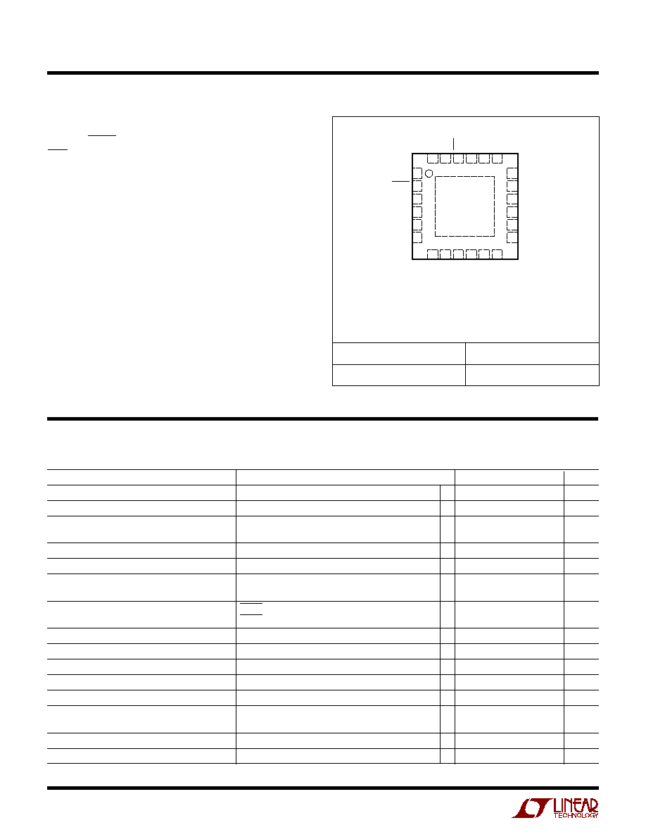
TOP VIEW
25
UF PACKAGE
24-LEAD (4mm
◊
4mm) PLASTIC QFN
10 11 12
6
5
4
3
2
1
13
14
15
16
17
18
FB
SHDN
V
REF
ENB
R
T
SS
V
OUTS
V
OUT
SW
SW
SW
PGND
V
C
LBI
LBO
V
IN
V
OUT
V
OUT
SYNC
I
LIM
BURST
GND
PGND
PGND
UF PART MARKING
3421
LTC3421
3
3421f
PARAMETER
CONDITIONS
MIN
TYP
MAX
UNITS
Frequency Accuracy
q
0.85
1
1.15
MHz
SYNC Input High
q
2.2
V
SYNC Input Low
q
0.8
V
SYNC Input Current
q
0.01
1
µ
A
ENB Input High
q
1.2
V
ENB Input Low
q
0.4
V
ENB Input Current
q
1
µ
A
SHDN Input High
V
OUT
= 0V (Initial Start-Up)
1.00
V
V
OUT
> 2.4V
0.65
V
SHDN Input Low
0.25
V
SHDN Input Current
q
0.01
1
µ
A
REF Output Voltage
q
1.183
1.22
1.257
V
REF Output Current Range
≠100
8
µ
A
Error Amp Transconductance
45
µ
s
LBI Threshold
Falling Edge
q
0.58
0.6
0.62
V
LBI Input Current
q
0.01
1
µ
A
LBO Low Voltage
V
IN
= 0V, I
SINK
= 1mA
12.0
50
mV
V
IN
= 0V, I
SINK
= 20mA
0.25
0.5
V
LBO Leakage
V
PGOOD
= 5.5V
0.01
1
µ
A
SS Current Source
V
SS
= 1V
1.2
2.4
5
µ
A
BURST Threshold Voltage
Falling Edge
0.87
0.97
1.07
V
ELECTRICAL CHARACTERISTICS
The
q
denotes the specifications which apply over the full operating
temperature range, otherwise specifications are at T
A
= 25
∞
C. V
IN
= 1.2V, V
OUT
= 3.3V, R
T
= 28k, unless otherwise noted.
Note 1: Absolute Maximum Ratings are those values beyond which the life
of a device may be impaired.
Note 2: The LTC3421E is guaranteed to meet performance specifications
from 0
∞
C to 70
∞
C. Specifications over the 40
∞
C to 85
∞
C operating
temperature range are assured by design, characterization and correlation
with statistical process controls.
Note 3: Current is measured into the V
OUTS
pin since the supply current is
bootstrapped to the output. The current will reflect to the input supply by
(V
OUT
/V
IN
) ∑ Efficiency. The outputs are not switching.
Note 4: Once V
OUT
is greater than 2.4V, the IC is not dependent on the V
IN
supply.
Note 5: This IC includes overtemperature protection that is intended to
protect the device during momentary overload conditions. Junction
temperature will exceed 125
∞
C when overtemperature protection is active.
Continuous operation above the specified maximum operating junction
temperature may impair device reliability.
LTC3421
4
3421f
TYPICAL PERFOR A CE CHARACTERISTICS
U
W
Single Cell to 3.3V Efficiency
OUTPUT CURRENT (mA)
30
EFFICIENCY (%)
90
100
20
10
80
50
70
60
40
0.1
10
100
1000
3421 G01
0
1
Burst Mode OPERATION
V
IN
= 1.5V
V
OUT
= 3.3V
f
OSC
= 1MHz
V
IN
= 1V
V
IN
= 1.2V
OUTPUT CURRENT (mA)
30
EFFICIENCY (%)
90
100
20
10
80
50
70
60
40
0.1
10
100
1000
3421 G02
0
1
Burst Mode OPERATION
V
IN
= 3V
V
OUT
= 3.3V
f
OSC
= 1MHz
V
IN
= 2.4V
V
IN
= 2V
OUTPUT CURRENT (mA)
30
EFFICIENCY (%)
90
100
20
10
80
50
70
60
40
0.1
10
100
1000
3421 G03
0
1
Burst Mode
OPERATION
V
OUT
= 5V
f
OSC
= 1MHz
V
IN
= 4.2V
V
IN
= 3.6V
V
IN
= 2.7V
2-Cell to 3.3V Efficiency
Li-Ion to 5V Efficiency
Burst Mode Operation
Load Transient Response
Inrush Current Control
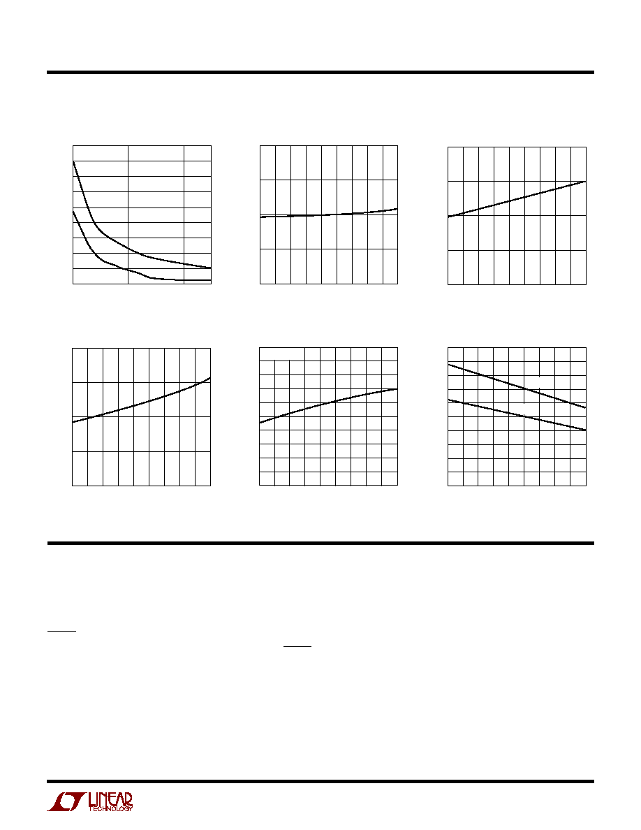
Efficiency vs Frequency
Efficiency vs V
IN
Start-Up Voltage vs Output Current
OUTPUT CURRENT (mA)
1
40
EFFICIENCY (%)
50
60
70
80
10
100
1000
3421 G07
30
20
10
0
90
100
V
IN
= 2.4V
V
OUT
= 3.3V
f = 300kHz
f = 3MHz
f = 1MHz
INPUT VOLTAGE (V)
1
0
EFFICIENCY (%)
10
30
40
50
100
70
2
3
3.5
3421 G08
20
80
90
60
1.5
2.5
4
4.5
5
V
IN
> V
OUT
PMOS LDO MODE
V
OUT
= 3.3V
I
OUT
= 200mA
OUTPUT CURRENT (mA)
0
START VOLTAGE (V)
1.00
1.05
1.10
200
3421 G09
0.95
0.90
0.80
50
100
150
0.85
1.20
1.15
V
OUT
50mV/DIV
AC COUPLED
INDUCTOR
CURRENT
0.5A/DIV
SW
2.5
µ
s/DIV
3421 G04
V
OUT
100mV/DIV
AC COUPLED
600mA
V
IN
= 2.4V
2.5ms/DIV
3421 G05
V
OUT
= 3.3V
C
OUT
= 44
µ
F
50mA
I
OUT
V
OUT
1V/DIV
INDUCTOR
CURRENT
0.5A/DIV
V
IN
= 0V TO 2.4V
500
µ
s/DIV
3421 G06
C
OUT
= 44
µ
F
(T
A
= 25
∞
C, unless otherwise specified)
LTC3421
5
3421f
Burst Mode Threshold vs R
BURST
FB Voltage
Frequency Accuracy
Burst Mode Quiescent Current
Current Limit Accuracy
R
DS(ON)
R
BURST
(k
)
20
0
OUTPUT CURRENT (mA)
20
60
80
100
INTO BURST
OUT OF BURST
120
180
3421 G10
40
70
120
140
160
TEMPERATURE (
∞
C)
≠45
1.20
VOLTAGE (V)
1.21
1.22
1.23
1.24
≠30 ≠15
0
15
3421 G11
30
45
60
75
90
TEMPERATURE (
∞
C)
≠45
0.95
FREQUENCY (MHz)
0.97
0.99
1.01
1.03
≠30 ≠15
0
15
3421 G12
30
45
60
75
90
TEMPERATURE (
∞
C)
≠45
0
CURRENT (
µ
A)
5
10
15
20
≠30 ≠15
0
15
3421 G13
30
45
60
75
90
FB (Pin 1): Feedback Pin. Connect resistor divider tap
here. The output voltage can be adjusted from 2.4V to
5.25V. The feedback reference voltage is typically 1.220V.
SHDN (Pin 2): Shutdown Pin. Less than 0.25V on this pin
shuts down the IC. The IC is enabled when the SHDN
voltage is greater than 1V. Once V
OUT
is above 2.2V,
hysteresis is applied to the pin (≠500nA out of the pin)
allowing it to operate at a logic high while the battery can
drop to 0.5V.
V
REF
(Pin 3): Buffered 1.22V Reference Output. This pin
can source up to 100
µ
A and sink up to 8
µ
A. This pin must
be decoupled with a 0.1
µ
F capacitor for stability.
PI FU CTIO S
U
U
U
ENB (Pin 4): Reference Output (V
REF
) and Low-Battery
Comparator Enable. When ENB = Low, the V
REF
output and
low-battery comparator are disabled, which lowers the
quiescent current by 5
µ
A. When ENB = High, the V
REF
output and the low-battery comparator are enabled. Dur-
ing shutdown, if the ENB = High and the output voltage is
pulled up to greater than 2.5V from a secondary source
such as a coin cell through a Schottky diode, the V
REF
output and low-battery comparator becomes powered
from the output voltage and enabled.
TEMPERATURE (
∞
C)
≠45
1.20
CURRENT (A)
1.25
1.35
1.40
1.45
1.70
1.55
≠15
15
30
90
3421 G14
1.30
1.60
1.65
1.50
≠30
0
45
60
75
R
LIM
= 105k
TEMPERATURE (
∞
C)
≠45
0
RESISTANCE (
)
0.02
0.06
0.08
0.10
0.20
0.14
≠15
15
30
90
3421 G15
0.04
0.16
0.18
0.12
≠30
0
45
60
75
PMOS
NMOS
TYPICAL PERFOR A CE CHARACTERISTICS
U
W
(T
A
= 25
∞
C, unless otherwise specified)

LTC3421
6
3421f
PI FU CTIO S
U
U
U
R
T
(Pin 5): Connect a resistor to ground to program the
oscillator frequency according to the formula:
f
R
OSC
T
=
28 100
,
where f
OSC
is in kHz and R
T
is in k
.
SS (Pin 6): Soft-Start Pin. Connect a capacitor from this
pin to ground to set the soft-start time according to the
formula:
t(ms) = C
SS
(
µ
F) ∑ 320
The nominal soft-start charging current is 2.5
µ
A. The
active range of SS is from 0.8V to 1.6V.
SYNC (Pin 7): Oscillator Synchronization Pin. A clock
pulse width of 100ns to 2
µ
s is required to synchronize the
internal oscillator. If not used SYNC should be grounded.
I
LIM
(Pin 8): Current Limit Adjust Pin. Connect a resistor
from this pin to ground to set the peak current limit thresh-
old for the N-channel MOSFET according to the formula
(note that this is the peak current in the inductor):
I
R
LIM
=
150
where I is in amps and R is in k
.
BURST (Pin 9): Burst Mode
Threshold Adjust Pin. A
resistor/capacitor combination from this pin to ground
programs the average load current at which automatic
Burst Mode operation is entered, according to the formula:
R
I
BURST
BURST
=
2
where R
BURST
is in k
and I
BURST
is in amps.
C
C
V
BURST
OUT
OUT
∑
,
10 000
where C
BURST(MIN)
and C
OUT
are in
µ
F.
For manual control of Burst Mode operation, ground the
BURST pin to force Burst Mode operation or connect it to
V
OUT
to force fixed frequency PWM mode. Note that the
BURST pin must not be pulled higher than V
OUT
.
GND (Pin 10): Signal Ground Pin. Connect to ground plane
near the R
T
resistor, error amp compensation compo-
nents and feedback divider.
PGND (Pins 11 to 13): Source Terminal of Power Internal
N-Channel MOSFET.
SW (Pins 14 to 16): Switch Pin for Inductor Connection.
For applications where V
OUT
> 4.3V, a Schottky diode from
SW to V
OUT
or to a snubber circuit is required to maintain
absolute maximum rating for SW. (see Application Cir-
cuits for 5V).
V
OUT
(Pins 17, 19 and 20): The output of the synchronous
rectifier and bootstrapped power source for the IC. A
ceramic bypass capacitor is required to be very close to
the V
OUT
and PGND pins of the IC.
V
OUTS
(Pin 18): V
OUT
Sense Pin. Connect V
OUTS
directly to
an output filter capacitor. The top of the feedback divider
network should also be tied to this point.
V
IN
(Pin 21): Input Supply Pin. Connect this pin to the
input supply and decouple with at least a 4.7
µ
F ceramic
capacitor.
LBO (Pin 22): Open-Drain Output. This pin pulls low when
the LBI input is below 0.6V. The open-drain output can
sink up to 20mA. During Burst Mode operation LBO is only
active during the time the IC wakes up to service the
output.
LBI (Pin 23): Low-Battery Comparator Input. Typical
threshold voltage is 0.6V with 30mV hysteresis. This
function is enabled when the ENB pin is high. The low-
battery comparator will operate off V
IN
or V
OUT
, whichever
is greater.
V
C
(Pin 24): Error Amp Output. A frequency compensation
network is connected from this pin to ground to compen-
sate the loop. See the section Compensating the Feedback
Loop for guidelines.
Exposed Pad (Pin 25): Ground. This pin must be soldered
to the PCB and is typically connected through the power
GND plane.

LTC3421
7
3421f
BLOCK DIAGRA
W
+
≠
+
≠
+
≠
+
PWM
LOGIC
CURRENT
COMP
ERROR
AMP
1.22V
CURRENT
LIMIT
+
+
Burst Mode
CONTROL
THERMAL
REG/SHDN
OSC
1.22V REF
2%
SLEEP
1%
UV
OV
OFF
≠3%
0.97V/1.05V
BURST
I/3000
3%
GND
≠
+
≠
+
≠
+
BURST
COMP
9
LBO
3421 BD
22
V
C
24
FB
1
I
LIM
SS
I
SENSE
AMP
NMOS
ANTICROSS
CONDUCTION
I
LIMIT
=
150k/R
C1
V
IN
V
DD
ANTIRING
≠
+
V
IN
WELL
SWITCH
I
ZERO
AMP
C
P
C
SS
R
Z
R2
R1
V
OUT
2.40V TO 5.25V
R
C1
8
V
OUT
17
V
OUT
19
V
OUT
20
6
SW
14
V
IN
1V TO 4.5V
21
ENB
V
OUT
4
V
REF
3
R
T
5
SYNC
V
IN
V
OUT
SYNC
IN
0.6V/
0.63V
7
LBI
R2
ENB
23
10
SHDN
SHUTDOWN
2
SW
15
SW
PMOS
16
V
OUTS
18
PGND
11
EXPOSED
PAD
25
PGND
12
PGND
13
SLOPE COMP
R1
≠
+

LTC3421
8
3421f
OPERATIO
U
LOW VOLTAGE START-UP
The LTC3421 includes an independent start-up oscillator
designed to start-up at input voltages of 0.85V typical. The
frequency and peak current limit during start-up are inter-
nally controlled. The device can start-up under some load
(see graph of Start-Up Current vs Input Voltage). Soft-
start and inrush current limiting are provided during start-
up as well as normal mode. The same soft-start capacitor
is used for each operating mode.
When either V
IN
or V
OUT
exceeds 2.25V, the IC enters
normal operating mode. Once the output voltage exceeds
the input by 0.3V, the IC powers itself from V
OUT
instead
of V
IN
. At this point the internal circuitry has no depen-
dency on the V
IN
input voltage, eliminating the require-
ment for a large input capacitor. The input voltage can drop
as low as 0.5V without affecting circuit operation. The
limiting factor for the application becomes the availability
of the power source to supply sufficient energy to the
output at the low voltages and the maximum duty cycle,
which is clamped at 91% typical.
LOW NOISE FIXED FREQUENCY OPERATION
Shutdown
The part is shut down by pulling SHDN below 0.3V, and
activated by pulling the pin initially above 1V and maintain-
ing a high state down to 0.5V. Note that the SHDN pin can
be driven above V
IN
or V
OUT
as long as it is limited to less
than the absolute maximum rating.
Soft-Start
The soft-start time is programmed with an external capaci-
tor to ground on the SS pin. An internal current source
charges it with a nominal 2.5
µ
A. The voltage on the SS pin
(in conjunction with the external resistor on the I
LIM
pin)
is used to control the peak current limit until the voltage on
the capacitor exceeds 1.6V, at which point the external
resistor sets the peak current. In the event of a com-
manded shutdown or a thermal shutdown, the capacitor is
discharged automatically. Note that Burst Mode operation
is inhibited during the soft-start time.
t(ms) = C
SS
(
µ
F) ∑ 320
Oscillator
The frequency of operation is set through a resistor from
the R
T
pin to ground. An internally trimmed timing capaci-
tor resides inside the IC. The oscillator can be synchro-
nized with an external clock applied to the SYNC pin. When
synchronizing the oscillator, the free running frequency
must be set to an approximately 30% lower frequency
than the desired synchronized frequency.
Current Sensing
Lossless current sensing converts the peak current signal
to a voltage to sum in with the internal slope compensa-
tion. This summed signal is compared to the error ampli-
fier output to provide a peak current control command for
the PWM. The slope compensation in the IC is adaptive to
the input voltage and output voltage. Therefore, the con-
verter provides the proper amount of slope compensation
to ensure stability, but not an excess to cause a loss of
phase margin in the converter.
Error Amplifier
The error amplifier is a transconductance amplifier, with
its positive input internally connected to the 1.22V refer-
ence and its negative input connected to FB. A simple
compensation network is placed from COMP to ground.
Internal clamps limit the minimum and maximum error
amplifier output voltage for improved large-signal tran-
sient response. During sleep (in Burst Mode operation),
the compensation pin is high impedance; however, clamps
limit the voltage on the external compensation network,
preventing the compensation capacitor from discharging
to zero during the sleep time.
Current Limit
The programmable current limit circuit sets the maximum
peak current. This clamp level is programmed with a
resistor from I
LIM
to ground. In Burst Mode operation, the
current limit is automatically set to a nominal value of 0.6A
peak for optimal efficiency.
I
R
LIM
=
150
where I is in amps and R is in k
.

LTC3421
9
3421f
OPERATIO
U
Zero Current Amplifier
The zero current amplifier monitors the inductor current to
the output and shuts off the synchronous rectifier once the
current is below 50mA typical, preventing negative induc-
tor current.
Antiringing Control
The antiringing control places a resistor across the
inductor to damp the ringing on the SW pin in discontinu-
ous conduction mode. The LC
SW
ringing (L = inductor,
C
SW
= capacitance on SW pin) is low energy, but can
cause EMI radiation.
V
REF
The internal 1.22V reference is buffered and brought out
to REFOUT. It is active when the ENB pin is pulled high
(above 1.4V). For stability, a minimum of a 0.1
µ
F capacitor
must be placed on the pin. The output can source up to
100
µ
A and sink up to 8
µ
A. For the lowest possible quies-
cent current in Burst Mode operation, the reference output
should be disabled by grounding the ENB pin.
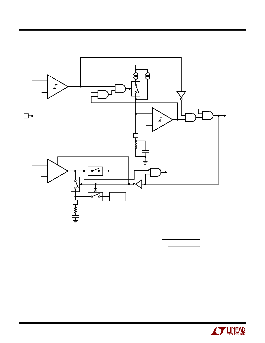
Burst Mode OPERATION
Burst Mode operation can be automatic or user controlled.
In automatic operation, the IC will automatically enter
Burst Mode operation at light load and return to fixed
frequency PWM mode for heavier loads. The user can
program the average load current at which the mode
transition occurs using a single resistor.
The oscillator is shut down in this mode, since the on time
is determined by the time it takes the inductor current to
reach a fixed peak current and the off time is determined
by the time it takes for the inductor current to return to
zero.
In Burst Mode operation, the IC delivers energy to the
output until it is regulated and then goes into a sleep mode
where the outputs are off and the IC is consuming only
12
µ
A of quiescent current. In this mode, the output ripple
has a variable frequency component with load current and
will be typically 2% peak-peak. This maximizes efficiency
at very light loads by minimizing switching and quiescent
losses. Burst Mode ripple can be reduced slightly by
increasing the output capacitance. Another method of
reducing Burst Mode ripple is to place a small feed-
forward capacitor across the upper resistor in the V
OUT
feedback divider network.
During Burst Mode operation, the V
C
pin is disconnected
from the error amplifier in an effort to hold the voltage on
the external compensation network where it was before
entering Burst Mode operation. To minimize the effects of
leakage current and stray resistance, voltage clamps limit
the min and max voltage on V
C
during Burst Mode opera-
tion. This minimizes the transient experienced when a
heavy load is suddenly applied to the converter after being
in Burst Mode operation for an extended period of time.
For automatic operation, an RC network should be con-
nected from BURST to ground. The value of the resistor
will control the average load current (I
BURST
) at which
Burst Mode operation will be entered and exited (there is
hysteresis to prevent oscillation between modes). The
equation given for the capacitor on BURST is for the
minimum value to prevent ripple on BURST from causing
the part to oscillate in and out of Burst Mode operation at
the current where the mode transition occurs.
R
I
BURST
BURST
=
2
where R
BURST
is in k
and I
BURST
is in amps.
C
C
V
BURST
OUT
OUT
∑
,
10 000
where C
BURST(MIN)
and C
OUT
are in
µ
F.
In the event that a sudden load transient causes FB to
deviate by more than 4% from the regulation value, an
internal pull-up is applied to BURST, forcing the part
quickly out of Burst Mode operation. For optimum tran-
sient response when going between Burst Mode operation
and PWM mode, the mode should be controlled manually
by the host. This way PWM mode can be commanded
before the load step occurs, minimizing output voltage
droop. For manual control of Burst Mode operation, the
RC network can be eliminated. To force fixed frequency
PWM mode, BURST should be connected to V
OUT
. To
force Burst Mode operation, BURST should be grounded.
LTC3421
10
3421f
OPERATIO
U
The circuit connected to BURST should be able to sink or
source up to 2mA. Note that Burst Mode operaton is
inhibited during start-up and soft-start.
Note that if V
IN
is above V
OUT
≠ 0.3V, the part will exit Burst
Mode operation and the synchronous rectifier will be
disabled.
Note that if the load applied during forced Burst Mode
operation exceeds the current that can be supplied, the
output voltage will start to droop and the part will auto-
matically come out of Burst Mode operation and enter fixed
frequency mode, raising V
OUT
. The maximum current that
can be supplied in Burst Mode operation is given by:
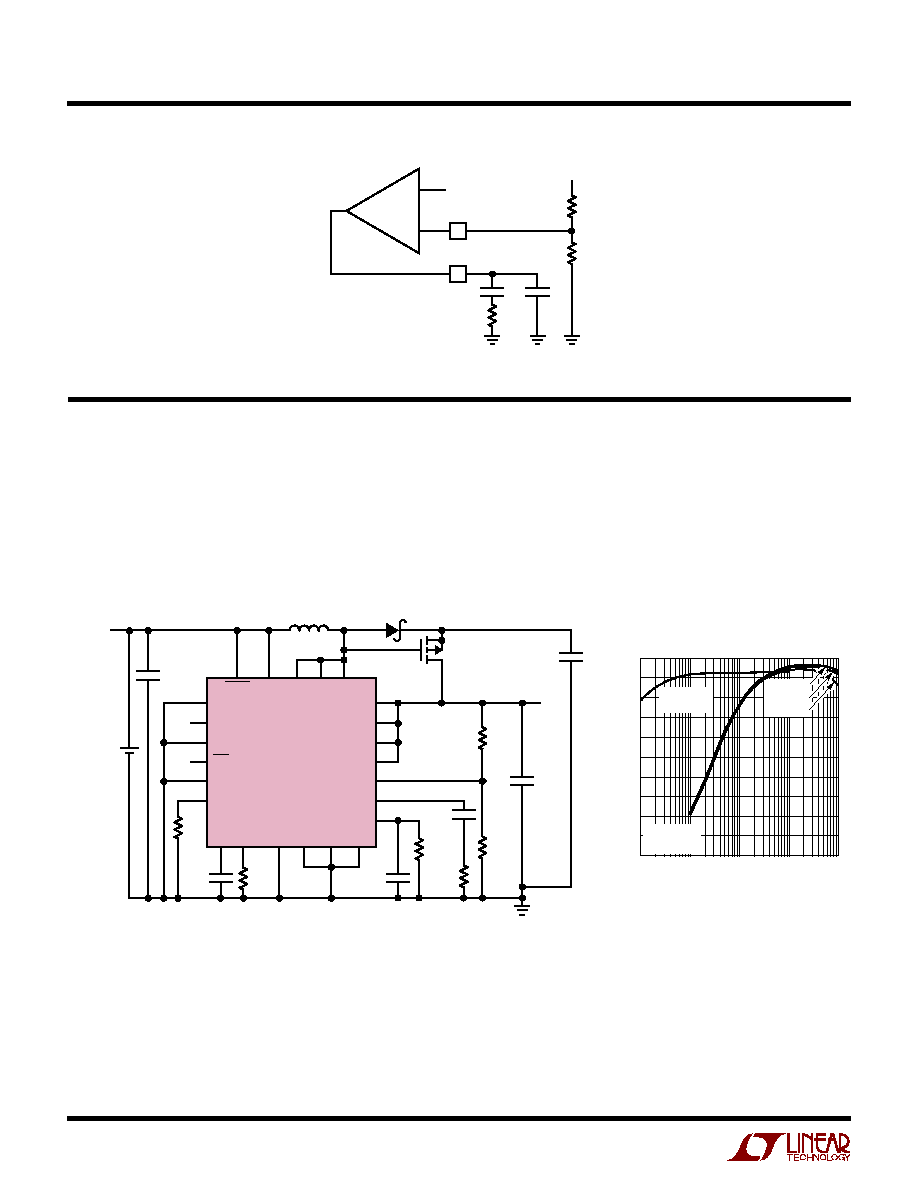
Simplified Diagram of Automatic Burst Mode Control Circuit
≠
+
24
TO
MODULATOR
CLAMP
0.5V TO 1V
SLEEP
3421 TA03
ERROR AMP/
SLEEP COMP
V
C
R
COMP
C
COMP
V
REF
±
1%
≠
+
≠
+
9 BURST
0.9V/
1.1V
R
B
C
B
SSDONE
MODE
1 = Burst Mode
OPERATION
0 = PWM MODE
SSDONE
V
REF
≠4%
UV
V
CC
1mA
I
OUT
/3000
1
FB
I
V
V
V
in amps
O MAX
OUT
IN
IN
(
)
.
∑
≠
=
+
(
)
0 55
2
1
OUTPUT DISCONNECT AND INRUSH LIMITING
The LTC3421 is designed to allow true output disconnect
by eliminating body diode conduction of the internal
P-channel MOSFET rectifier. This allows V
OUT
to go to zero
volts during shutdown without drawing any current from
the input source. It also allows for inrush current limiting
at turn-on, minimizing surge currents seen by the input
supply. Note that to obtain the advantages of output
LTC3421
11
3421f
OPERATIO
U
disconnect, there must not be any external Schottky
diodes connected between the SW pins and V
OUT
.
Note: Board layout is extremely critical to minimize volt-
age overshoot on the SW pins due to stray inductance.
Keep the output filter capacitors as close as possible to the
V
OUT
pins and use very low ESR/ESL ceramic capacitors,
tied to a good ground plane. In V
OUT
> 4.3V applications,
a Schottky diode is required from the switch nodes to V
OUT
to limit the peak switch voltage to less than 6V unless
some form of external snubbing is employed. (See 5V
Applications section.)
APPLICATIO S I FOR ATIO
W
U
U
U
COMPONENT SELECTION
Inductor Selection
The high frequency operation of the LTC3421 allows the
use of small surface mount inductors. The minimum
inductance value is proportional to the operating fre-
quency and is limited by the following constraints:
L
f
and L
V
V
V
f Ripple V
IN MIN
OUT MAX
IN MIN
OUT MAX
>
>
(
)
3
(
)
(
)
(
)
(
)
∑
≠
∑
∑
24
23
22
21
20
19
7
8
9
10
11
12
13
18
17
16
15
14
6
1
2
3
4
5
FB
V
C
LBI
LBO
V
IN
V
OUT
V
OUT
V
OUT
SYNC I
LIM
BURST GND PGND PGND
GND
3421 F01
MULTIPLE VIAS
TO GROUND
PLANE
SHDN
V
REF
ENB
R
T
SS
V
OUTS
V
OUT
SW
SW
SW
PGND
V
IN
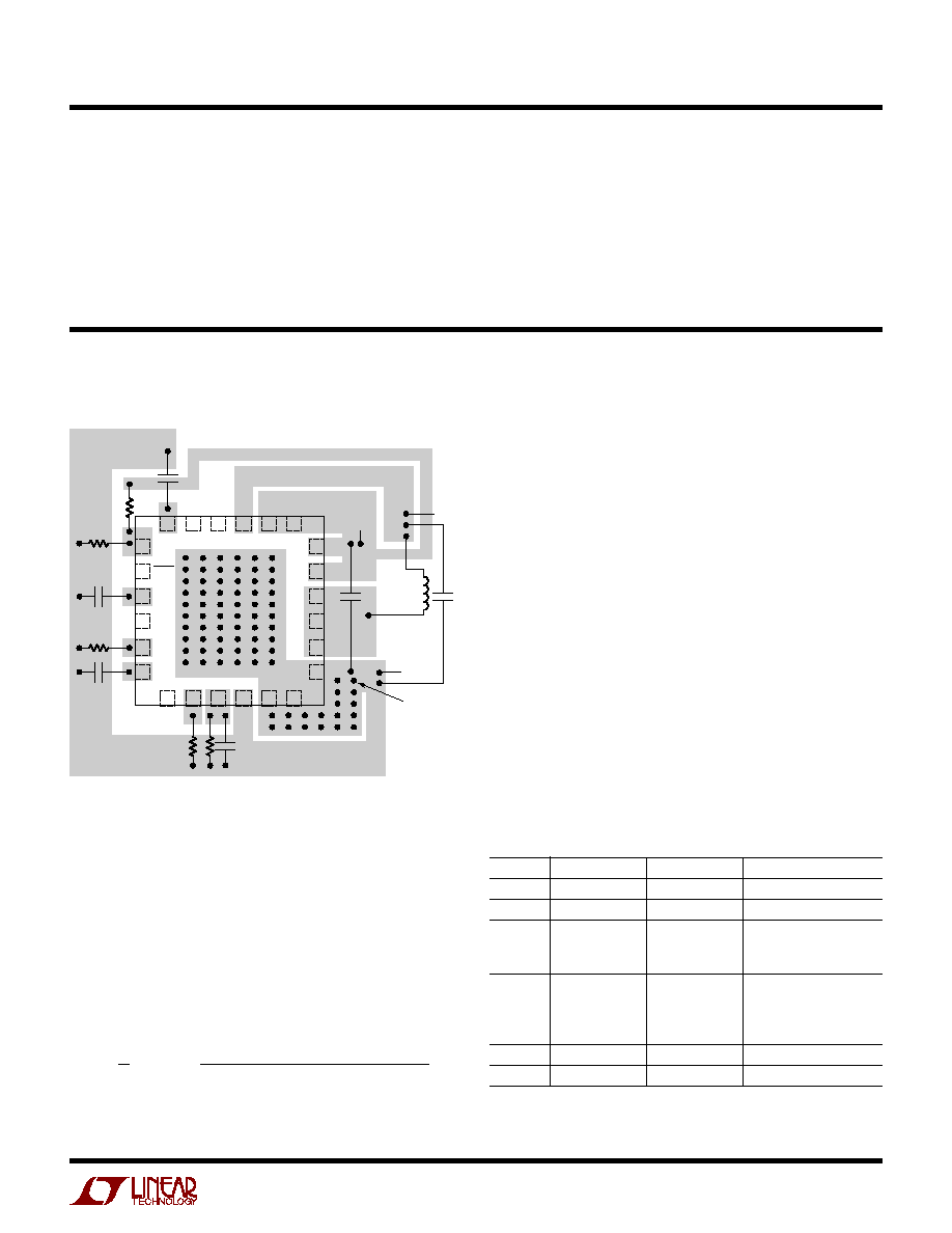
Figure 1. Recommended Component Placement. Traces Carrying
High Current are Direct (PGND, SW, V
OUT
). Trace Area at FB and
V
C
are Kept Low. Lead Length to Battery Should be Kept Short.
V
IN
and V
OUT
Ceramic Capacitors Should be as Close to the IC
Pins as Possible
where
f = Operating Frequency in MHz
Ripple = Allowable Inductor Current Ripple (Amps
Peak-Peak)
V
IN(MIN)
= Minimum Input Voltage
V
OUT(MAX)
= Maximum Output Voltage
The inductor current ripple is typically set to 20% to 40%
of the maximum inductor current.
For high efficiency, choose an inductor with high fre-
quency core material, such as ferrite, to reduce core loses.
The inductor should have low ESR (equivalent series
resistance) to reduce the I
2
R losses and must be able to
handle the peak inductor current without saturating. Molded
chokes or chip inductors usually do not have enough core
to support peak inductor currents in the 1A to 4A region.
To minimize radiated noise, use a toroidal or shielded
inductor. See Table 1 for suggested inductor suppliers and
Table 2 for a list of capacitor suppliers.
Table 1. Inductor Vendor Information
SUPPLIER PHONE
FAX
WEB SITE
Coilcraft
(847) 639-6400
(847) 639-1469 www.coilcraft.com
Coiltronics (561) 241-7876
(516) 241-9339
Murata
USA:
USA:
www.murata.com
(814) 237-1431
(814) 238-0490
(800) 831-9172
Sumida
USA:
USA:
www.sumida.com
(847) 956-0666
(847) 956-0702
Japan:
Japan:
81-3-3607-5111 81-3-3607-5144
TDK
(847) 803-6100
(847) 803-6296 www.component.tdk.com
TOKO
(847) 297-0070
(847) 669-7864 www.toko.com
LTC3421
12
3421f
APPLICATIO S I FOR ATIO
W
U
U
U
Output Capacitor Selection
The output voltage ripple has two components to it. The
bulk value of the capacitor is set to reduce the ripple due
to charge into the capacitor each cycle. The maximum
ripple due to charge is given by:
V
I
V
C
V
f
RBULK
P
IN
OUT
OUT
=
∑
∑
∑
where I
P
= peak inductor current.
The ESR (equivalent series resistance) is usually the most
dominant factor for ripple in most power converters. The
ripple due to capacitor ESR is simply given by:
V
RCESR
= I
P
∑ C
ESR
where C
ESR
= capacitor series resistance.
Low ESR capacitors should be used to minimize output
voltage ripple. For surface mount applications, AVX TPS
series tantalum capacitors, Sanyo POSCAP or Taiyo Yuden
ceramic capacitors are recommended. For through-hole
applications, Sanyo OS-CON capacitors offer low ESR in a
small package size.
In some layouts it may be necessary to place a 1
µ
F low ESR
ceramic capacitor as close to the V
OUT
and GND pins as
possible.
Input Capacitor Selection
The input filter capacitor reduces peak currents drawn
from the input source and reduces input switching noise.
Since the IC can operate at voltages below 0.5V once the
output is regulated, the demand on the input capacitor is
much less. In most applications 1
µ
F per amp of peak input
current is recommended. Taiyo Yuden offers very low ESR
ceramic capacitors, for example the 1
µ
F in a 0603 case
(JMK107BJ105MA).
Table 2. Capacitor Vendor Information
SUPPLIER
PHONE
FAX
WEB SITE
AVX
(803) 448-9411 (803) 448-1943 www.avxcorp.com
Sanyo
(619) 661-6322 (619) 661-1055 www.sanyovideo.com
TDK
(847) 803-6100 (847) 803-6296 www.component.tdk.com
Murata
USA:
USA:
www.murata.com
(814) 237-1431 (814) 238-0490
(800) 831-9172
Taiyo Yuden (408) 573-4150 (408) 573-4159 www.t-yuden.com
Operating Frequency Selection
There are several considerations in selecting the operating
frequency of the converter. The first is, which are the sen-
sitive frequency bands that cannot tolerate any spectral
noise? The second consideration is the physical size of the
converter. As the operating frequency goes up, the induc-
tor and filter capacitors go down in value and size. The trade
off is in efficiency since the switching losses due to gate
charge are going up proportional with frequency.
Another operating frequency consideration is whether the
application can allow "pulse skipping." In this mode, the
minimum on time of the converter cannot support the duty
cycle, so the converter ripple will go up and there will be
a low frequency component of the output ripple. In many
applications where physical size is the main criterion,
running the converter in this mode is acceptable. In appli-
cations where it is preferred not to enter this mode, the
maximum operating frequency is given by:
f
V
V
V
t
Hz
MAX NOSKIP
OUT
IN
OUT
ON MIN
_
(
)
≠
∑
=
where t
ON(MIN)
= minimum on time = 120ns.
Thermal Considerations
To deliver the power that the LTC3421 is capable of, it is
imperative that a good thermal path be provided to
dissipate the heat generated within the package. This can
be accomplished by taking advantage of the large thermal
pad on the underside of the IC. It is recommended that mul-
tiple vias in the printed circuit board be used to conduct
heat away from the IC and into a copper plane with as much
area as possible. In the event that the junction tempera-
ture gets too high, the peak current limit will automatically
be decreased. If the junction temperature continues to rise,
the part will go into thermal shutdown, and all switching
will stop until the temperature drops.
V
IN
> V
OUT
Operation
The LTC3421 will maintain voltage regulation when the
input voltage is above the output voltage. This is achieved
by terminating the switching on the synchronous PMOS
and applying V
IN
statically on the gate. This will ensure the
LTC3421
13
3421f
APPLICATIO S I FOR ATIO
W
U
U
U
volts ∑ seconds of the inductor will reverse during the time
current is flowing to the output. Since this mode will
dissipate more power in the IC, the maximum output
current is limited in order to maintain an acceptable
junction temperature.
I
T
V
V
OUT MAX
A
IN
OUT
(
)
≠
∑
.
≠
=
+
(
)
(
)
125
40
1 5
where T
A
= ambient temperature.
For example at V
IN
= 4.5V and V
OUT
= 3.3V, the maximum
output current is 370mA.
Short Circuit
The LTC3421 output disconnect feature allows output short
circuit while maintaining a maximum set current limit. The
IC has incorporated internal features such as current limit
and thermal shutdown for protection from an excessive
overload or short circuit. In applications that require a pro-
longed short circuit, it is recommended to limit the power
dissipation in the IC to maintain an acceptable junction
temperature. The circuit in Figure 2 will limit the maximum
current during a prolonged short by reducing the current
limit value in a short circuit by disconnecting R2 with the
N-channel MOSFET switch. R3 and C1 provide a soft-start
function after a short circuit. Resistor R1 lowers the cur-
rent limit value as V
IN
rises, maintaining a relatively con-
stant power. The current limit equation for the circuit in
Figure 2 is given by:
I
R
V
R
LIMIT
LIM
IN
=
0 6
0 6
1
250
.
≠
≠ .
∑
where I
LIMIT
is in Amps; R
LIM
and R1 are in k
.
Closing the Feedback Loop
The LTC3421 uses current mode control with internal
adaptive slope compensation. Current mode control elimi-
nates the 2nd order filter due to the inductor and output
capacitor exhibited in voltage mode controllers, and sim-
plifies it to a single pole filter response. The product of the
modulator control to output DC gain and the error amp
open-loop gain gives the DC gain of the system:
G
G
V
V
G
V
I
G
DC
EA
REF
OUT
CONTROL
IN
OUT
EA
=
=
G
CONTROL_OUTPUT
∑
∑
∑
,
2
2000
The output filter pole is given by:
f
I
V
C
FILTER POLE
OUT
OUT
OUT
_
∑
∑
=
where C
OUT
is the output filter capacitor.
The output filter zero is given by:
f
R
C
FILTER ZERO
ESR
OUT
_
∑
∑
∑
=
1
2
where R
ESR
is the capacitor equivalent series resistance.
A troublesome feature of the boost regulator topology is
the right-half plane zero (RHP) and is given by:
f
V
I
L
RHPZ
IN
OUT
=
2
2 ∑
∑
∑
At heavy loads this gain increase with phase lag can occur
at a relatively low frequency. The loop gain is typically
rolled off before the RHP zero frequency.
The typical error amp compensation is shown in Figure 3.
The equations for the loop dynamics are as follows:
f
e
C
f
R
C
f
R
C
POLE
C
ZERO
Z
C
POLE
Z
C
1
1
1
1
2
2
1
2
20 6
1
2
1
2
∑
∑
∑
∑
∑
∑
∑
∑
∑
which is extremely close to DC
Figure 2. Current Limit Foldback Circuit for
Extended Short Conditions
8
R2
50k
C1
0.1
µ
F
3421 F02
R1
1M
R3
10k
R
LIM
100k
VN2222
I
LIM
TO V
IN
TO V
OUT
LTC3421
14
3421f
5V Applications
When the output voltage is programmed above 4.3V it is
necessary to add a Schottky diode either from SW to
V
OUT
, or to a snubber network in order to maintain an
acceptable peak voltage on SW. The Schottky to the
output will provide a peak efficiency improvement but will
negate the output disconnect feature. If output disconnect
is required, the Schottky to an active snubber network is
suggested as shown in Figure 4.
Figure 4. Lithium-Ion to 5V at 1A Application with an Active Snubber Circuit
TYPICAL APPLICATIO
U
OUTPUT CURRENT (mA)
30
EFFICIENCY (%)
90
100
20
10
80
50
70
60
40
0.1
10
100
1000
3421 G03
0
1
Burst Mode
OPERATION
V
OUT
= 5V
f
OSC
= 1MHz
V
IN
= 4.2V
V
IN
= 3.6V
V
IN
= 2.7V
Li-Ion to 5V Efficiency
SHDN
ENB
V
REF
LBI
LBO
SYNC
I
LIM
V
OUTS
V
OUT
V
OUT
V
OUT
FB
V
C
BURST
V
IN
SW SW
L1
3
µ
H
SW
18
17
19
20
1
24
9
13
12
11
10
5
6
8
7
22
23
3
4
2
21
14
15
16
SS
R
T
GND
LTC3421
C2
0.1
µ
F
C3
0.1
µ
F
C4
470pF
C5*
22
µ
F
◊
2
C6*
1
µ
F
C1*
10
µ
F
V
IN
2.7V TO
4.2V
Li-Ion
R2
28k
R3
10k
R4
100k
R5
1.13M
M1
D1*
V
OUT
5V
1A
R6
365k
3421 F04
R1
60k
*LOCATE COMPONENTS CLOSE TO PINS
C1: TAIYO YUDEN JMK212BJ106MM
C5: TAIYO YUDEN JMK325BJ226MM
PGND PGND PGND
+
D1: MOTOROLA MBR0520L
L1: SUMIDA CDRH6D28-3R0
M1: ZETEX ZXM61P025
Figure 3
1
≠
+
1.22V
C
C1
C
C2
R
Z
3421 F03
R2
R1
ERROR
AMP
FB
V
OUT
24
V
C
APPLICATIO S I FOR ATIO
W
U
U
U
LTC3421
15
3421f
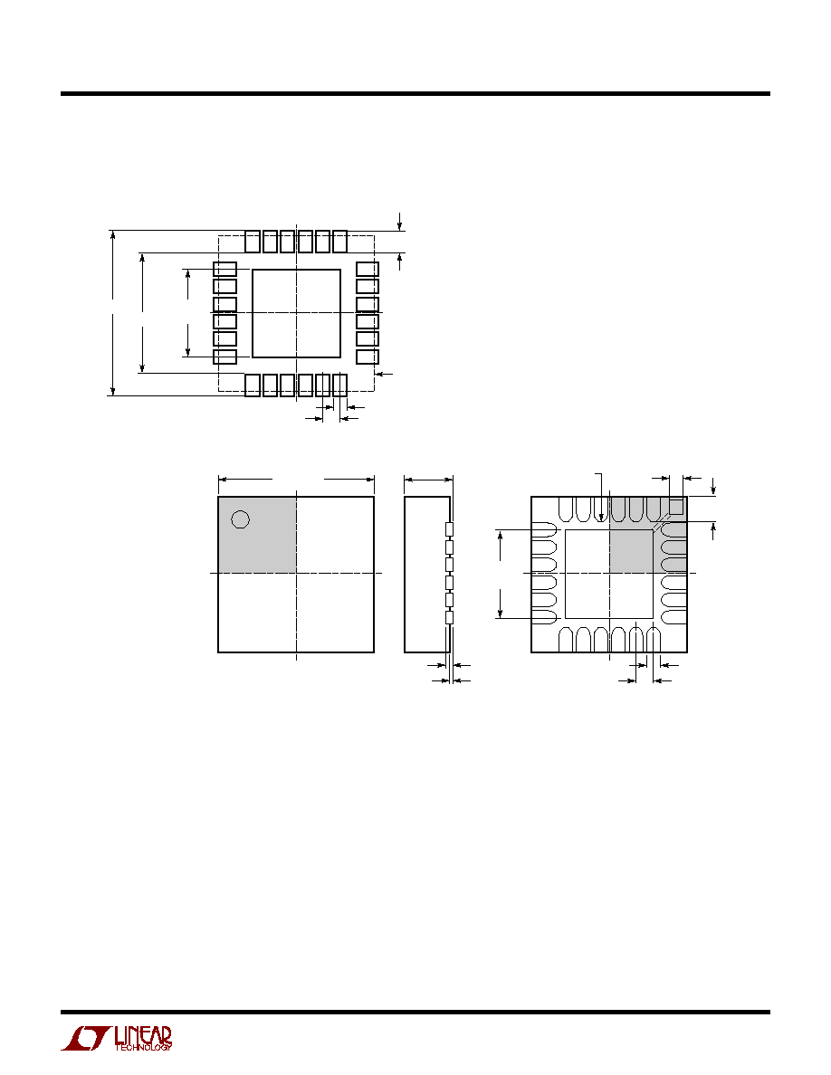
PACKAGE DESCRIPTIO
U
UF Package
24-Lead Plastic QFN (4mm
◊
4mm)
(Reference LTC DWG # 05-08-1697)
4.00
±
0.10
(4 SIDES)
NOTE:
1. DRAWING PROPOSED TO BE MADE A JEDEC PACKAGE OUTLINE MO-220 VARIATION (WGGD-X)--TO BE APPROVED
2. ALL DIMENSIONS ARE IN MILLIMETERS
3. DIMENSIONS OF EXPOSED PAD ON BOTTOM OF PACKAGE DO NOT INCLUDE
MOLD FLASH. MOLD FLASH, IF PRESENT, SHALL NOT EXCEED 0.15mm ON ANY SIDE, IF PRESENT
4. EXPOSED PAD SHALL BE SOLDER PLATED
5. SHADED AREA IS ONLY A REFERENCE FOR PIN 1 LOCATION
ON THE TOP AND BOTTOM OF PACKAGE
6. DRAWING NOT TO SCALE
PIN 1
TOP MARK
(NOTE 5)
0.38
±
0.10
24
0.23 TYP
(4 SIDES)
23
1
2
BOTTOM VIEW--EXPOSED PAD
2.45
±
0.10
(4-SIDES)
0.75
±
0.05
R = 0.115
TYP
0.25
±
0.05
0.50 BSC
0.200 REF
0.00 ≠ 0.05
(UF24) QFN 0603
RECOMMENDED SOLDER PAD PITCH AND DIMENSIONS
0.70
±
0.05
0.25
±
0.05
0.50 BSC
2.45
±
0.05
(4 SIDES)
3.10
±
0.05
4.50
±
0.05
PACKAGE OUTLINE
Information furnished by Linear Technology Corporation is believed to be accurate and reliable.
However, no responsibility is assumed for its use. Linear Technology Corporation makes no represen-
tation that the interconnection of its circuits as described herein will not infringe on existing patent rights.
LTC3421
16
3421f
Linear Technology Corporation
1630 McCarthy Blvd., Milpitas, CA 95035-7417
(408) 432-1900
q
FAX: (408) 434-0507
q
www.linear.com
©
LINEAR TECHNOLOGY CORPORATION 2003
LT/TP 1103 1K PRINTED IN USA
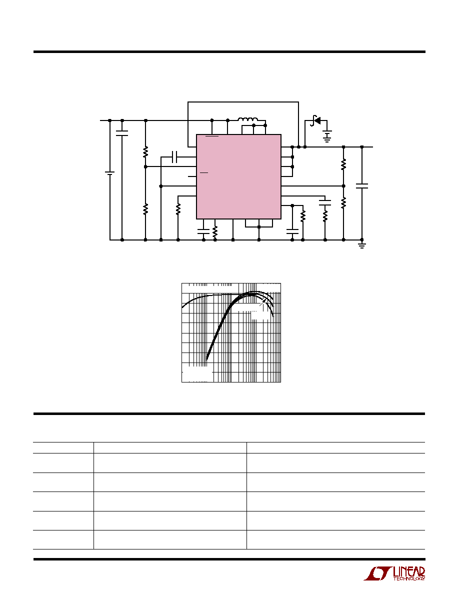
TYPICAL APPLICATIO
U
Single Cell to 3.3V at 500mA with Secondary Cell Backup During Shutdown. LOWBAT and V
REF
Output are Enabled
SHDN
ENB
V
REF
LBI
LBO
SYNC
I
LIM
V
OUTS
V
OUT
V
OUT
V
OUT
FB
V
C
BURST
V
IN
2
21
14
15
16
18
17
19
20
1
24
9
13
12
11
10
5
6
8
7
22
23
3
4
SW SW
L1
4.7
µ
H
SW
SS
R
T
GND
LTC3421
C2
0.1
µ
F
C3
0.1
µ
F
C4
470pF
C5*
22
µ
F
C1*
4.7
µ
F
V
IN
1V TO 1.5V
1 CELL
PRIMARY CELL
LOW BAT
OUTPUT
R2
28k
R3
40k
R4
100k
R5
340k
3V
SECONDARY CELL
V
OUT
3.3V
500mA
R6
200k
3421 TA05
R1
60k
604k
301k
0.1
µ
F
*LOCATE COMPONENTS CLOSE TO PINS
C1: TAIYO YUDEN JMK212BJ106MM
PGND PGND PGND
D1
+
+
C5: TAIYO YUDEN JMK325BJ226MM
L1: TOKO A916CY-4R7M
RELATED PARTS
PART NUMBER
DESCRIPTION
COMMENTS
LT1371/LT1371HV
3A (I
SW
), 500kHz, High Efficiency Step-Up DC/DC
V
IN
: 2.7V to 30V, V
OUT(MAX)
: 35V/42V, I
Q
: 4mA, I
SD
: <12
µ
A,
Converters
DD, TO220-7, S20
LTC3400/LTC3400B
600mA (I
SW
), 1.2MHz, Synchronous Step-Up DC/DC
92% Efficiency, V
IN
: 0.85V to 5V, V
OUT(MAX)
: 5V, I
Q
: 19
µ
A/300
µ
A,
Converters
I
SD
: <1
µ
A, ThinSOT
LTC3401
1A (I
SW
), 3MHz, Synchronous Step-Up DC/DC Converter
97% Efficiency, V
IN
: 0.5V to 5V, V
OUT(MAX)
: 5.5V, I
Q
: 38
µ
A,
I
SD
: <1
µ
A, MS10
LTC3402
2A (I
SW
), 3MHz, Synchronous Step-Up DC/DC Converter
97% Efficiency, V
IN
: 0.5V to 5V, V
OUT(MAX)
: 5.5V, I
Q
: 38
µ
A,
I
SD
: <1
µ
A, MS10
LTC3425
5A (I
SW
), 8MHz, 4-Phase Synchronous Step-Up
95% Efficiency, V
IN
: 0.5V to 4.5V, V
OUT(MAX)
: 5.25V, I
Q
: 12
µ
A,
DC/DC Converter
8MHz, Low Ripple in QFN
OUTPUT CURRENT (mA)
30
EFFICIENCY (%)
90
100
20
10
80
50
70
60
40
0.1
10
100
1000
3421 G01
0
1
Burst Mode OPERATION
V
IN
= 1.5V
V
OUT
= 3.3V
f
OSC
= 1MHz
V
IN
= 1V
V
IN
= 1.2V
Single Cell to 3.3V Efficiency