 | –≠–ª–µ–∫—Ç—Ä–æ–Ω–Ω—ã–π –∫–æ–º–ø–æ–Ω–µ–Ω—Ç: LTC3459 | –°–∫–∞—á–∞—Ç—å:  PDF PDF  ZIP ZIP |
LTC3459
1
3459f
, LTC and LT are registered trademarks of Linear Technology Corporation.
s
Small Solution Size
s
>85% Efficiency over Wide Load Range
s
Internal Synchronous Rectifier
s
V
IN
Range: 1.5V to 5.5V
s
5V at 30mA from 3.3V Input
s
3.3V at 20mA from 2 AA Cell Input
s
Programmable Output Voltages Up to 10V
s
Burst Mode
Æ
Operation
s
Inrush Current Limiting
s
Output Disconnect in Shutdown
s
Ultralow Quiescent (10
µ
A) and Shutdown
(< 1
µ
A) Currents
s
Low Profile (1mm) SOT-23 Package
10V Micropower
Synchronous Boost Converter
in ThinSOT
s
General Purpose Micropower Boost
s
Digital Cameras
s
PDAs
s
LCD Bias
s
Small OLED Displays
s
Supercap Charging
Burst Mode is a registered trademark of Linear Technology Corporation.
ThinSOT is trademark of Linear Technology Corporation.
The LTC
Æ
3459 is a low current, high efficiency synchronous
boost converter intended for low power, size constrained
portable applications. The LTC3459 can be powered from
a single lithium ion battery, a 2- to 3-cell stack of Alkaline
or Nickel batteries, or any low impedance voltage source
between 1.5V and 5.5V. The output is programmable via
an external divider between 2.5V and 10V. Although the part
is primarily intended for boost applications, V
OUT
will
maintain regulation below V
IN
(at reduced efficiency).
The LTC3459 offers Burst Mode operation with a fixed
peak current, providing high conversion efficiency over a
wide range of load currents. During start-up, inductor
current is controlled preventing the inrush surge current
found in many boost converters. In shutdown the output
is disconnected from the input and quiescent current is
reduced to <1
µ
A.
The LTC3459 is offered in a low profile (1mm) 6-pin
SOT-23 (ThinSOT
TM
) package allowing a tiny footprint for
the total solution.
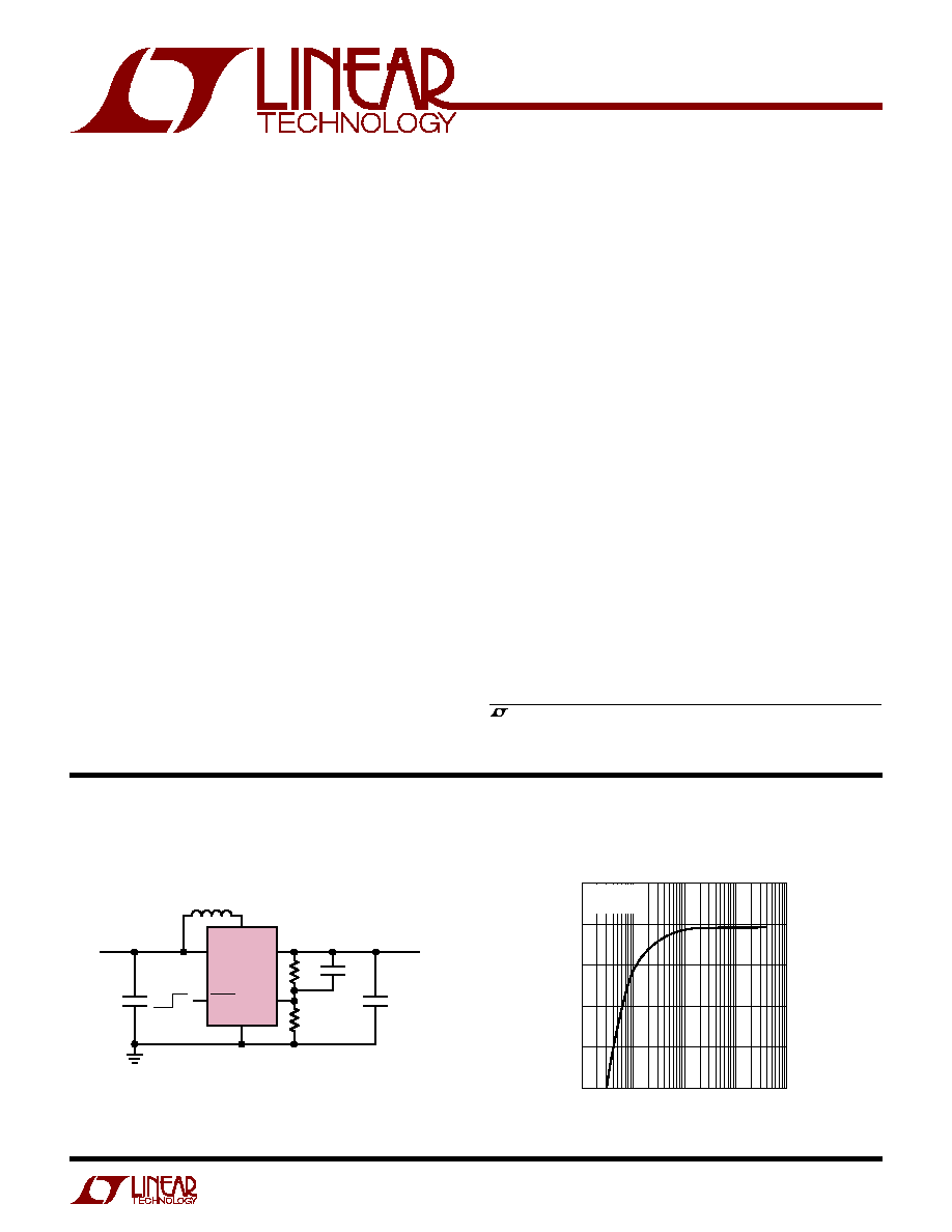
SW
22
µ
H
V
IN
2M
47pF
V
OUT
8V
30mA
4.7
µ
F
1
µ
F
5V
LTC3459
SHDN
V
OUT
FB
OFF ON
GND
365k
3459 TA01a
5V to 8V Converter
I
LOAD
(mA)
60
EFFICIENCY (%)
70
80
90
100
0.01
1
10
100
3459 TA01b
50
0.1
V
IN
= 5V
V
OUT
= 8V
Efficiency
FEATURES
DESCRIPTIO
U
APPLICATIO S
U
TYPICAL APPLICATIO
U

LTC3459
2
3459f
V
IN
, FB Voltage ........................................... ≠ 0.3V to 7V
V
OUT
, SHDN Voltage ................................. ≠ 0.3V to 10V
SW Voltage ............................................... ≠ 0.3V to 12V
Operating Temperature Range
(Notes 2, 3) ........................................ ≠ 40
∞
C to 85
∞
C
Storage Temperature Range ................ ≠ 65
∞
C to 150
∞
C
Lead Temperature (Soldering, 10 sec)................. 300
∞
C
ORDER PART
NUMBER
Referred to GND (Note 1)
ABSOLUTE AXI U RATI GS
W
W
W
U
PACKAGE/ORDER I FOR ATIO
U
U
W
Consult LTC Marketing for parts specified with wider operating temperature ranges.
LTC3459ES6
T
JMAX
= 125
∞
C,
JA
= 165
∞
C/W,
JC
= 102
∞
C/W
S6 PART MARKING
LTAHA
The
q
denotes the specifications which apply over the full operating
temperature range, otherwise specifications are at T
A
= 25
∞
C. V
IN
= 3.3V, V
OUT
= 5V, unless otherwise noted.
ELECTRICAL CHARACTERISTICS
SW 1
GND 2
FB 3
6 V
IN
5 V
OUT
4 SHDN
TOP VIEW
S6 PACKAGE
6-LEAD PLASTIC TSOT-23
Note 1: Absolute Maximum Ratings are those values beyond which the life
of a device may be impaired.
Note 2: The LTC3459E is guaranteed to meet performance specifications
from 0
∞
C to 70
∞
C. Specifications over the ≠ 40
∞
C to 85
∞
C operating
temperature range are assured by design, characterization and correlation
with statistical process controls.
Note 3: This IC includes overtemperature protection that is intended to
protect the device during momentary overload conditions. Junction
temperature will exceed 125
∞
C when overtemperature protection is active.
Continuous operation above the specified maximum operating junction
temperature may impair device reliability.
PARAMETER
CONDITIONS
MIN
TYP
MAX
UNITS
V
IN
Input Voltage Range
q
1.5
5.5
V
V
IN
Quiescent Current
SHDN = V
CC
10
20
µ
A
V
IN
Shutdown Current
SHDN = GND
0.1
1
µ
A
V
OUT
Programmable Voltage Range
q
2.5
10
V
V
OUT
Quiescent Supply Current
SHDN = V
CC
2
4
µ
A
V
OUT
Shutdown Current
SHDN = GND
0.1
1
µ
A
Reference
Feedback Voltage
V
IN
= 3.3V, V
OUT
= 7.5V
q
1.19
1.22
1.25
V
FB Input Leakage Current
Measured on FB
10
50
nA
Converter Performance
Peak Switch Current (V
IN
= 3.3V)
L = 22
µ
H
q
60
75
90
mA
t
OFF
Timer (V
IN
= 3.3V, V
OUT
= 5V)
Varies by 1/(V
OUT
≠ V
IN
)
225
400
550
ns
Zero Current Comparator Threshold
L = 22
µ
H
0
mA
Main NMOS Switch
On Resistance
V
OUT
= 5V
2.8
Leakage Current
V
SWITCH
= 10V, V
OUT
= 10V
0.01
1
µ
A
Main PMOS Switch
On Resistance
V
OUT
= 5V
4.2
Leakage Current
V
IN
= 5V, V
SWITCH
= 5V, V
OUT
= 0V
0.02
2
µ
A
Logic Inputs
SHDN Threshold (Rising Edge)
0.3
1
V
SHDN Hysteresis
80
mV
SHDN Input Leakage Current
0
50
nA

LTC3459
3
3459f
TYPICAL PERFOR A CE CHARACTERISTICS
U
W
Minimum R
OUT
vs V
IN
V
IN
(V)
1.5
R
OUT
(
)
3500
3
3459 G01
2000
1000
2
2.5
3.5
500
0
4000
3000
2500
1500
4
4.5
5.5
5
V
OUT
= 10V
V
OUT
= 7.5V
V
OUT
= 5V
V
OUT
= 3.3V
L = 22
µ
H
V
IN
(V)
1.5
200
250
400
350
3
4
3459 G02
150
100
2
2.5
3.5
4.5
5.5
5
50
0
300
P
OUT
(mW)
V
OUT
= 10V
V
OUT
= 7.5V
V
OUT
= 5V
V
OUT
= 3.3V
L = 22
µ
H
TEMPERATURE (
∞
C)
≠40
CURRENT (
µ
A)
14
20
3459 G03
8
4
≠ 20
0
40
2
0
16
V
IN
= 3.3V
V
OUT
= 5V
I
IN
I
OUT
12
10
6
60
80
Minimum P
OUT
vs V
IN
V
IN
and V
OUT
Quiescent Current
vs Temperature
Switching Frequency
vs V
IN
at Various V
OUTS
V
IN
(V)
1.5
FREQUENCY (MHz)
2.0
2.5
3.0
3
4
5.5
3459 G04
1.5
1.0
0.5
2
2.5
3.5
4.5
5
V
OUT
= 10V
V
OUT
= 7.5V
V
OUT
= 5V
V
OUT
= 3.3V
L = 22
µ
H
V
IN
(V)
1.5
% CHANGE IN V
OUT
0
1.0
5.5
3459 G05
≠1.0
≠2.0
2.5
3.5
4.5
2
3
4
5
2.0
≠0.5
0.5
≠1.5
1.5
4.7
µ
F
10
µ
F
22
µ
F
47
µ
F
V
OUT
= 5V
L = 22
µ
H
TEMPERATURE (
∞
C)
≠40
R
DS(ON)
(
)
4
5
6
20
60
3459 G06
3
2
≠20
0
40
NCH
PCH
80
1
0
V
OUT
= 5V
V
OUT
Regulation vs V
IN
and C
OUT
N-Channel and P-Channel
MOSFET R
DS(ON)
vs Temperature
Shutdown Threshold Voltage
vs Temperature
TEMPERATURE (
∞
C)
≠40
SHUTDOWN THRESHOLD VOLTAGE (V)
0.8
1.0
1.2
20
60
3459 G07
0.6
0.4
≠20
0
40
80
0.2
0
SHDN FALLING
SHDN RISING
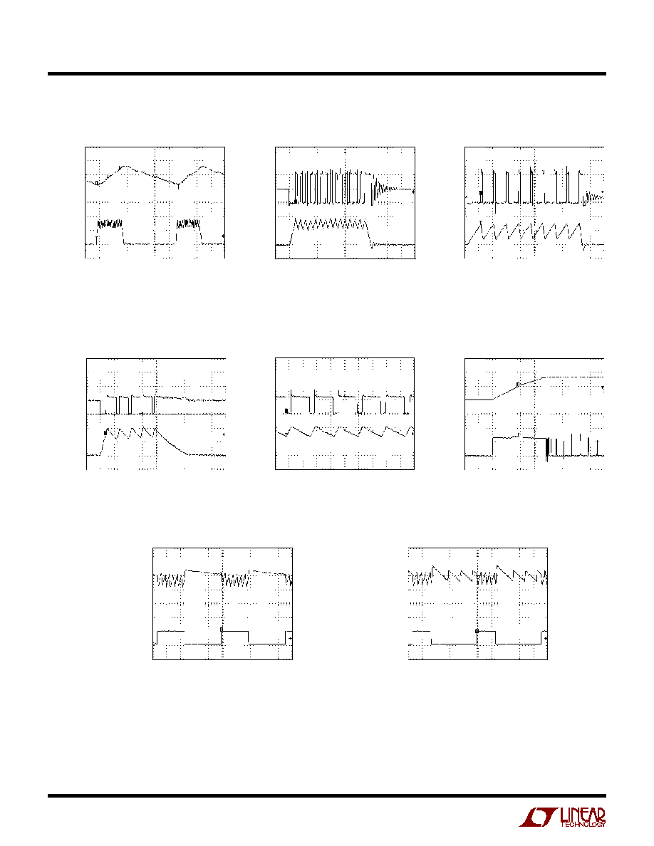
Burst Cycle
SW
CURRENT
50mA/DIV
INDUCTOR
CURRENT
50mA/DIV
V
IN
= 3.3V
V
OUT
= 5V
L = 22
µ
H
1
µ
s/DIV
3459 G08
SW
CURRENT
50mA/DIV
INDUCTOR
CURRENT
50mA/DIV
V
IN
= 3.3V
V
OUT
= 5V
L = 22
µ
H
100ns/DIV
3459 G09
Switch Pin Waveform
(T
A
= 25
∞
C unless otherwise noted.)
LTC3459
4
3459f
V
OUT
AC Ripple
V
OUT
50mV/DIV
INDUCTOR
CURRENT
50mA/DIV
V
IN
= 3.3V
V
OUT
= 5V
L = 22
µ
H
C
OUT
= 4.7
µ
F
C
FF
= 47pF
5
µ
s/DIV
3459 G10
Burst Cycle
SW
CURRENT
50mA/DIV
INDUCTOR
CURRENT
50mA/DIV
V
IN
= 5V
V
OUT
= 10V
L = 22
µ
H
1
µ
s/DIV
3459 G11
SW
CURRENT
50mA/DIV
INDUCTOR
CURRENT
50mA/DIV
V
IN
= 2V
V
OUT
= 10V
L = 22
µ
H
1
µ
s/DIV
3459 G12
Burst Cycle
V
OUT
Regulated Below V
IN
Burst
Cycle
Shorted Output
Start-Up
SW
CURRENT
50mA/DIV
INDUCTOR
CURRENT
50mA/DIV
V
IN
= 5V
V
OUT
= 3.5V
L = 22
µ
H
1
µ
s/DIV
3459 G13
V
IN
= 5V
V
OUT
= 0V
L = 22
µ
H
500ns/DIV
3459 G14
SW
CURRENT
50mA/DIV
INDUCTOR
CURRENT
50mA/DIV
V
IN
= 3.6V
V
OUT
= 0V TO 8V
L = 22
µ
H
C
IN
= 2.2
µ
F
250
µ
s/DIV
3459 G15
V
OUT
VOLTAGE
50mA/DIV
INPUT
CURRENT
50mA/DIV
Load Steps
Load Steps
V
OUT
AC RIPPLE
50mV/DIV
WITH 50k
(TRACE 2
GROUNDED)
TO 500
(TRACE 2 = 5V)
V
IN
= 3.6V
V
OUT
= 8V
L = 22
µ
H
C
OUT
= 4.7
µ
F
C
FF
= 47pF
100
µ
s/DIV
3459 G16
V
IN
= 3.6V
V
OUT
= 8V
L = 22
µ
H
C
OUT
= 4.7
µ
F
C
FF
= 47pF
100
µ
s/DIV
3459 G17
V
OUT
AC RIPPLE
50mV/DIV
WITH 5k
(TRACE 2
GROUNDED)
TO 500
(TRACE 2 = 5V)
TYPICAL PERFOR A CE CHARACTERISTICS
U
W
(T
A
= 25
∞
C unless otherwise noted.)

LTC3459
5
3459f
U
U
U
PI FU CTIO S
SW (Pin 1): Switch Pin. Connect a 15
µ
H to 33
µ
H inductor
between SW and V
IN
. Keep PCB trace lengths as short and
wide as possible to reduce EMI and voltage overshoot. If
the inductor current falls to zero, the internal P-channel
MOSFET synchronous rectifier is turned off to prevent
reverse charging of the inductor.
GND (Pin 2): Signal and Power Ground. Provide a short,
direct PCB path between GND and the (≠) side of the filter
capacitors on V
IN
and V
OUT
.
FB (Pin 3): Input to the Burst Mode Comparator. An
external resistor divider connected between V
OUT
, GND
and this pin sets the output voltage to:
V
OUT
= 1.22(1 + R1/R2)
SHDN (Pin 4): Master Shutdown Input. Driving SHDN low
disables all IC functions and reduces quiescent current
from the battery to less than 2
µ
A. This pin must be pulled
above 1V to enable the IC.
V
OUT
(Pin 5): Regulated Output Voltage of the Boost
Regulator. Bypass V
OUT
with a low ESR, ESL ceramic
capacitor between 2.2
µ
F and 10
µ
F. V
OUT
ripple increases
with smaller capacitors.
V
IN
(Pin 6): Input Supply Pin. Bypass V
IN
with a low ESR,
ESL ceramic capacitor of at least 1
µ
F.