 | ÐлекÑÑоннÑй компоненÑ: LTC3499 | СкаÑаÑÑ:  PDF PDF  ZIP ZIP |
3499f.pm65
LTC3499/LTC3499B
1
3499f
4.7
µH
3499 TA01
LTC3499
SW
FB
GND
V
IN
V
OUT
SHDN
VC
SS
OFF
ON
10
µF
V
OUT
5V
175mA
V
IN
1.8V TO 3.2V
1M
324k
0.01
µF
330pF
100k
2.2
µF
+
The LTC
®
3499/LTC3499B are synchronous, fixed fre-
quency step-up DC/DC power converters with integrated
reverse battery protection that protect and disconnect the
devices and load when the battery polarity is reversed while
delivering high efficiency in a small (3mm
× 3mm) DFN
package. True output disconnect eliminates inrush current
and allows zero load current in shutdown.
The devices feature an input voltage range of 1.8V to 5.5V
enabling operation from two alkaline or NiMH batteries.
The switching frequency is internally set at 1.2MHz allow-
ing the use of tiny surface mount inductors and capacitors.
A minimal number of external components are required to
generate output voltages ranging from 2V to 6V. The
LTC3499 features automatic Burst Mode operation to
increase efficiency at light loads, while the LTC3499B
features continuous switching at light loads.
The soft-start time is externally programmable through a
small capacitor. Anti-ring circuitry reduces EMI emissions
by damping the inductor in discontinuous mode. The
devices feature <1
µA shutdown supply current, integrated
overvoltage protection and are available in both 8-pin
(3mm
× 3mm) DFN and 8-pin MSOP packages.
Medical Equipment
Digital Cameras
MP3 Players
Handheld Instruments
APPLICATIO S
U
TYPICAL APPLICATIO
U
DESCRIPTIO
U
750mA Synchronous
Step-Up DC/DC Converters
with Reverse-Battery Protection
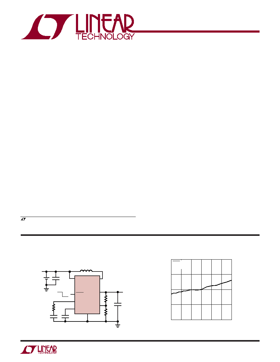
Two AA Cells to 5V Synchronous Boost Converter
Battery Current vs V
IN
FEATURES
Reverse-Battery Protection for DC/DC Converter
and Load
High Efficiency: Up to 94%
Generates 5V at 175mA from a 1.8V Input
Operates from 1.8V to 5.5V Input Supply
2V to 6V Adjustable Output Voltage
Inrush Current Controlled During Start-Up
Output Disconnnect in Shutdown
Low Noise 1.2MHz PWM Operation
Tiny External Components
Automatic Burst Mode
®
Operation (LTC3499)
Continuous Switching at Light Loads (LTC3499B)
Overvoltage Protection
8-Lead (3mm
× 3mm × 0.75mm) DFN
and MSOP Packages
, LTC and LT are registered trademarks of Linear Technology Corporation.
Burst Mode is a registered trademark of Linear Technology Corporation.
All other trademarks are the property of their respective owners.
V
IN
AND SW VOLTAGE (V)
6
1.0
BATTERY CURRENT (
µ
A)
0
2
2
4
0
4
3499 TA01b
6
0.5
1.0
0.5
SHDN = 0V
V
OUT
= 0V
LTC3499/LTC3499B
3499f
2
ABSOLUTE AXI U
RATI GS
W
W
W
U
(Note 1)
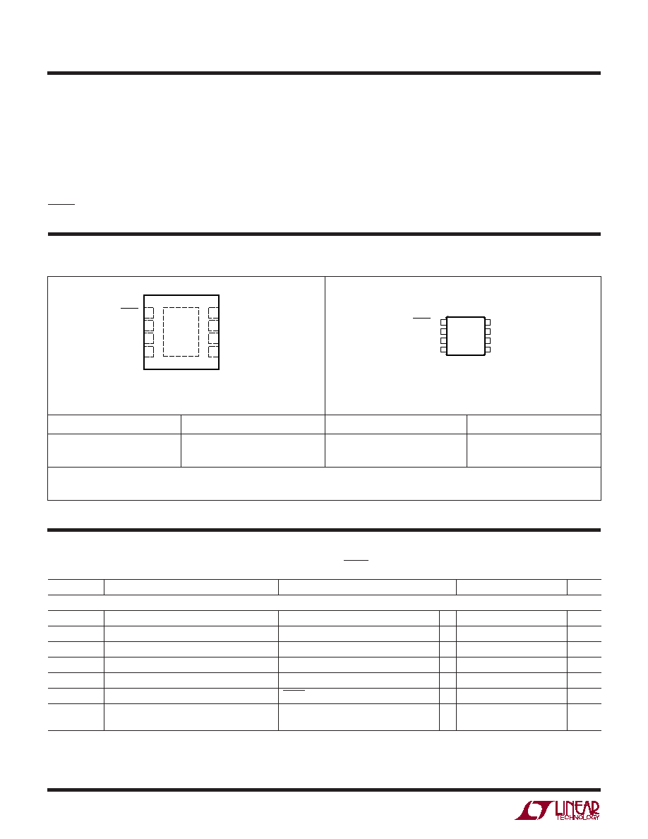
TOP VIEW
DD PACKAGE
8-LEAD PLASTIC DFN
5
6
7
8
4
3
2
1
SHDN
V
IN
SW
GND
VC
FB
V
OUT
SS
9
PACKAGE/ORDER I FOR ATIO
U
U
W
FB, SS to GND ............................................ 0.3V to 7V
Operating Temperature Range
(Notes 3, 4) ........................................ 40
°C to 85°C
Storage Temperature Range ................ 65
°C to 125°C
Lead Temperature (Soldering, 10 sec)
MSOP .............................................................. 300
°C
ELECTRICAL CHARACTERISTICS
The
denotes specifications that apply over the full operating temperature
range, otherwise specifications are at T
A
= 25
°C. V
IN
= 2.4V, V
OUT
= 5V, SHDN = 2.4V, T
A
= T
J
unless otherwise noted.
V
IN
to GND ..................................................... 7V to 7V
V
OUT
to GND ............................................... 0.3V to 7V
SW to V
OUT
.................................................... 7V to 1V
SW to GND
DC .............................................................. 7V to 7V
Pulsed < 100ns .......................................... 7V to 8V
SHDN to GND ................................................ 7V to 7V
ORDER PART NUMBER
LTC3499EDD
LTC3499BEDD
LTC3499EMS8
LTC3499BEMS8
1250
Consult LTC Marketing for parts specified with wider operating temperature ranges.
VC
FB
V
OUT
SS
SHDN
V
IN
SW
GND
1
2
3
4
8
7
6
5
TOP VIEW
MS8 PACKAGE
8-LEAD PLASTIC MSOP
T
JMAX
= 125
°C,
JA
= 160
°C/W
DD PART MARKING
SYMBOL
PARAMETER
CONDITIONS
MIN
TYP
MAX
UNITS
Supply
V
IN
Minimum Start-Up Voltage
1.6
1.8
V
V
OUT
Output Voltage Adjust Range
2
6
V
V
FB
FB Voltage
1.195
1.220
1.245
V
I
FB
FB Input Current
V
FB
= 1.22V
3
50
nA
I
VIN
V
IN
Quiescent Current
No Output Load
300
600
µA
I
SD
V
IN
Quiescent Current in Shutdown
SHDN = 0V, V
OUT
= 0V
0.1
1
µA
I
BURST
Quiescent Current Burst Mode Operation
V
IN
Current at 2.4V (LTC3499 Only)
20
µA
V
OUT
Current at 5V (LTC3499 Only)
1.5
µA
T
JMAX
= 125
°C,
JA
= 45
°C
EXPOSED PAD (PIN 9) IS GND, MUST BE SOLDERED TO PCB
Order Options Tape and Reel: Add #TR Lead Free: Add #PBF Lead Free Tape and Reel: Add #TRPBF
Lead Free Part Marking:
http://www.linear.com/leadfree/
ORDER PART NUMBER
MS8 PART MARKING
LBRB
LCDZ
LTBRC
LTCFB
LTC3499/LTC3499B
3
3499f
ELECTRICAL CHARACTERISTICS
The
denotes specifications that apply over the full operating temperature
range, otherwise specifications are at T
A
= 25
°C. V
IN
= 2.4V, V
OUT
= 5V, SHDN = 2.4V, T
A
= T
J
unless otherwise noted.
Note 1: Stresses beyond those listed under Absolute Maximum Ratings
may cause permanent damage to the device. Exposure to any Absolute
Maximum Rating condition for extended periods may affect device
reliability and lifetime.
Note 2: Specification is guaranteed by design and not 100% tested in
production.
Note 3:The LTC3499E/LTC3499BE are guaranteed to meet device
specifications from 0
°C to 85°C. Specifications over the 40°C to 85°C
operating temperature are assured by design, characterization and
correlation with statistical process controls.
Note 4: These ICs include overtemperature protection that is intended to
protect the devices during momentary overload conditions. Junction
temperatures will exceed 125
°C when overtemperature protection is
active. Continuous operation above the specified maximum operating
temperature range may impair device reliability.
SYMBOL
PARAMETER
CONDITIONS
MIN
TYP
MAX
UNITS
I
NMOS
NMOS Switch Leakage
V
SW
= 6V
0.1
5
µA
I
PMOS
PMOS Switch Leakage
V
OUT
= 6V, V
SW
= 0V
0.1
5
µA
R
NMOS
NMOS Switch On Resistance
V
OUT
= 3.3V
0.45
V
OUT
= 5V
0.4
R
PMOS
PMOS Switch On Resistance
V
OUT
= 3.3V
0.58
V
OUT
= 5V
0.45
I
LIM
NMOS Current Limit
0.75
A
t
DLY, ILIM
Current Limit Delay to Output
Note 2
60
ns
D
MAX
Maximum Duty Cycle
80
85
%
D
MIN
Minimum Duty Cycle
0
%
f
OSC
Frequency Accuracy
1
1.2
1.4
MHz
G
mEA
Error Amplifier Transconductance
40
µmhos
I
SOURCE
Error Amplifier Source Current
5
µA
I
SINK
Error Amplifier Sink Current
5
µA
I
SS
SS Current Source
V
SS
= 1V
3
µA
V
OV
V
OUT
Overvoltage Threshold
6.8
V
V
OV(HYST)
V
OUT
Overvoltage Hysteresis
400
mV
Shutdown
V
SHDN(LOW)
SHDN Input Low
0.2
V
V
SHDN(HIGH)
SHDN Input High
Measured at SW
1.2
V
I
SD
SHDN Input Current
1
µA
Reverse Battery
I
VOUT,REVBATT
V
OUT
Reverse-Battery Current
V
OUT
= 0V, V
IN
= V
SHDN
= V
SW
= 6V
5
µA
I
VIN,REVBATT
V
IN
and V
SW
Reverse-Battery Current
V
OUT
= 0V, V
IN
= V
SHDN
= V
SW
= 6V
5
µA
I
SHDN,REVBATT
SHDN Reverse-Battery Current
V
OUT
= 0V, V
IN
= V
SHDN
= V
SW
= 6V
5
µA
LTC3499/LTC3499B
3499f
4
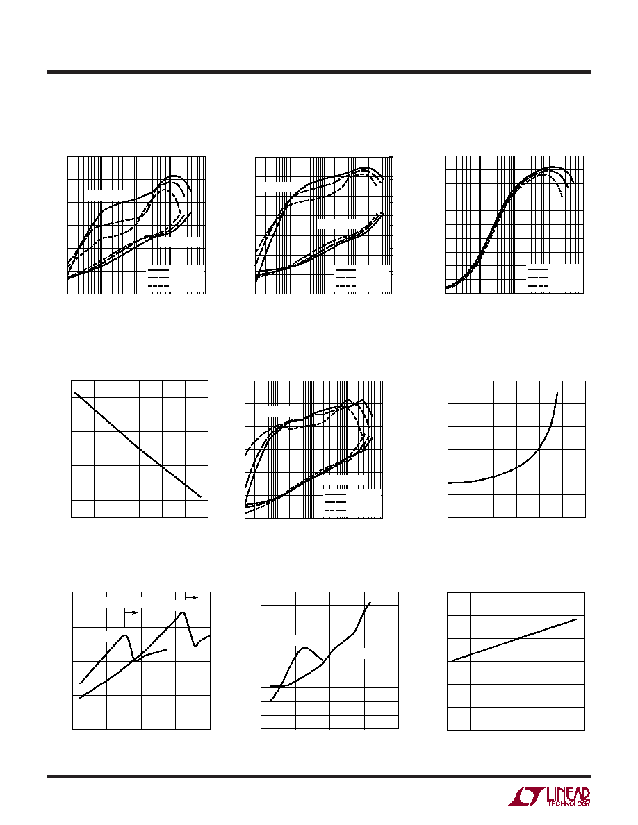
TYPICAL PERFOR A CE CHARACTERISTICS
U
W
2-Cell to 5V Efficiency
vs Load Current (LTC3499 Only)
T
A
= 25
°C unless noted.
LOAD CURRENT (mA)
0.1
40
EFFICIENCY (%)
POWER LOSS (mW)
50
60
70
80
90
100
0.1
1
10
100
1000
10000
100000
1
10
100
1000
3499 G01
V
IN
= 3.2V
V
IN
= 2.4V
V
IN
= 1.8V
POWER LOSS
EFFICIENCY
LOAD CURRENT (mA)
0.1
70
80
100
100
3499 G03
60
50
1
10
1000
40
30
90
100
1000
100000
10
1
0.1
10000
EFFICIENCY (%)
POWER LOSS (mW)
V
IN
= 4.2V
V
IN
= 3.6V
V
IN
= 3V
POWER LOSS
EFFICIENCY
Li-Ion to 5V Efficiency
vs Load Current (LTC3499 Only)
LOAD CURRENT (mA)
0.1
40
EFFICIENCY (%)
POWER LOSS (mW)
50
60
70
80
90
100
0.1
1
10
100
1000
10000
100000
1
10
100
1000
3499 G02
V
IN
= 3V
V
IN
= 2.4V
V
IN
= 1.8V
POWER LOSS
EFFICIENCY
Maximum Output Current
Capability vs V
IN
No Load Input Current vs V
IN
(LTC3499 Only)
Burst Mode Quiescent Current
vs Temperature (LTC3499 Only)
Current Limit Accuracy
vs Temperature
Burst Mode Output Current
Threshold vs Input Voltage
(LTC3499 Only)
2-Cell to 3.3V Efficiency
vs Load Current (LTC3499 Only)
TEMPERATURE (
°C)
50
CURRENT LIMIT (A)
1.00
1.01
1.02
25
75
3499 G04
0.99
0.98
0.97
0.96
25
0
50
1.03
1.04
100
INPUT VOLTAGE (V)
1.8
0
Burst Mode OUTPUT CURRENT THRESHOLD (mA)
10
20
30
40
60
2.3
2.8
3.3
3.8
3499 G05
4.3
4.8
50
V
OUT
= 5V
V
IN
(V)
1.5
OUTPUT CURRENT (mA)
400
500
600
5.5
3499 G06
300
200
0
2.5
3.5
4.5
100
800
700
V
OUT
= 3.3V
V
OUT
= 5V
V
IN
> V
OUT
V
IN
> V
OUT
V
IN
(V)
1.5
0
INPUT CURRENT (
µ
A)
20
60
80
100
200
140
2.5
3.5
3499 G07
40
160
180
120
4.5
5.5
V
OUT
= 3.3V
V
OUT
= 5V
TEMPERATURE (
°C)
50
0
Burst Mode QUIESCENT CURRENT (
µ
A)
5
10
15
20
30
25
0
25
50
3499 G08
75
100
25
LOAD CURRENT (mA)
30
EFFICIENCY (%)
90
100
20
10
80
50
70
60
40
0.1
10
100
1000
3499 G17
0
1
V
IN
= 3.2V
V
IN
= 2.4V
V
IN
= 1.8V
2-Cell to 5V Efficiency
vs Load Current (LTC3499B Only)
LTC3499/LTC3499B
5
3499f
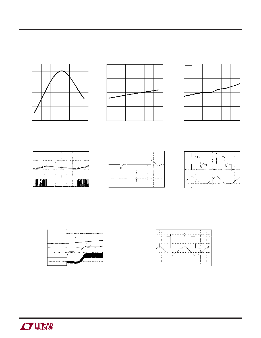
Fixed Frequency Discontinous
Mode Operation
Soft-Start into 25
Load
Load Transient 50mA to 200mA
TYPICAL PERFOR A CE CHARACTERISTICS
U
W
T
A
= 25
°C unless noted.
Fixed Frequency Operation
Oscillator Frequency
vs Temperature
TEMPERATURE (
°C)
50
1.0
OSCILLATOR FREQUENCY (MHz)
1.1
1.2
1.3
1.4
25
0
25
50
3499 G08
75
100
V
IN
and SW Reverse-Battery
Current vs V
IN
and SW Voltage
V
OUT
50mV/DIV
20
µs/DIV
3499 G12
V
IN
= 2.4V
V
OUT
= 5V
L = 4.7
µH
C
OUT
= 10
µF
C
FF
= 10pF (FEEDFORWARD CAPACITOR FROM
V
OUT
TO FB)
I
L
50mA/DIV
Burst Mode Operation
(LTC3499 Only)
V
OUT
200mV/DIV
200
µs/DIV
3499 G13
V
IN
= 2.4V
V
OUT
= 5V
I
LOAD
= 50mA to 200mA
R
Z
= 100k
C
F
= 680pF
C
OUT
= 10
µF
L = 4.7
µH
I
LOAD
100mA/DIV
200mA
50mA
V
IN
2V/DIV
SS
2V/DIV
V
OUT
2V/DIV
1ms/DIV
34991G15
V
IN
= 2.4V
V
OUT
= 5V
L = 4.7
µH
C
SS
= 0.01
µF
C
OUT
= 10
µF
I
L
200mA/DIV
V
IN
AND SW VOLTAGE (V)
6
1.0
REVERSE-BATTERY CURRENT (
µ
A)
0
2
2
4
0
4
3499 G11
6
0.5
1.0
0.5
SHDN = 0V
V
OUT
= 0V
SW
2V/DIV
200ns/DIV
3499 G14
V
IN
= 2.4V
V
OUT
= 5V
L = 4.7
µH
I
L
100mA/DIV
SW
2V/DIV
200ns/DIV
3499 G16
V
IN
= 2.4V
V
OUT
= 5V
L = 4.7
µH
I
L
100mA/DIV
FB Voltage vs Temperature
TEMPERATURE (
°C)
50
FB VOLTAGE (V)
25
75
3499 G09
25
0
50
1.2215
1.2210
1.2205
1.2200
1.2195
1.2190
1.2185
1.2220
1.2225
100