 | ÐлекÑÑоннÑй компоненÑ: LTC3717 | СкаÑаÑÑ:  PDF PDF  ZIP ZIP |
Äîêóìåíòàöèÿ è îïèñàíèÿ www.docs.chipfind.ru
1
LTC3717
sn3717 3717fs
Wide Operating Range,
No R
SENSE
TM
Step-Down Controller
for DDR/QDR Memory Termination
s
V
OUT
= 1/2 V
IN
(Supply Splitter)
s
Adjustable and Symmetrical Sink/Source
Current Limit up to 20A
s
±
0.65% Output Voltage Accuracy
s
Up to 97% Efficiency
s
No Sense Resistor Required
s
Ultrafast Transient Response
s
True Current Mode Control
s
2% to 90% Duty Cycle at 200kHz
s
t
ON(MIN)
100ns
s
Stable with Ceramic C
OUT
s
Dual N-Channel MOSFET Synchronous Drive
s
Power Good Output Voltage Monitor
s
Wide V
CC
Range: 4V to 36V
s
Adjustable Switching Frequency up to 1.5MHz
s
Output Overvoltage Protection
s
Optional Short-Circuit Shutdown Timer
s
Available in a 16-Pin Narrow SSOP Package
s
Bus Termination: DDR and QDR Memory, SSTL,
HSTL, ...
s
Notebook Computers, Desktop Servers
s
Tracking Power Supply
The LTC
®
3717 is a synchronous step-down switching
regulator controller for double data rate (DDR) and Quad
Data Rate
TM
(QDR
TM
) memory termination. The controller
uses a valley current control architecture to deliver very
low duty cycles without requiring a sense resistor. Oper-
ating frequency is selected by an external resistor and is
compensated for variations in V
IN
.
Forced continuous operation reduces noise and RF inter-
ference. Output voltage is internally set to half of V
REF
,
which is user programmable.
Fault protection is provided by an output overvoltage
comparator and optional short-circuit shutdown timer.
Soft-start capability for supply sequencing is accom-
plished using an external timing capacitor. The regulator
current limit level is symmetrical and user programmable.
Wide supply range allows operation from 4V to 36V at the
V
CC
input.
, LTC and LT are registered trademarks of Linear Technology Corporation.
No R
SENSE
is a trademark of Linear Technology Corporation.
QDR RAMs and Quad Data Rate RAMs comprise a new family of products developed by Cypress
Semiconductor, Hitachi, IDT, Micron Technology, Inc. and Samsung.
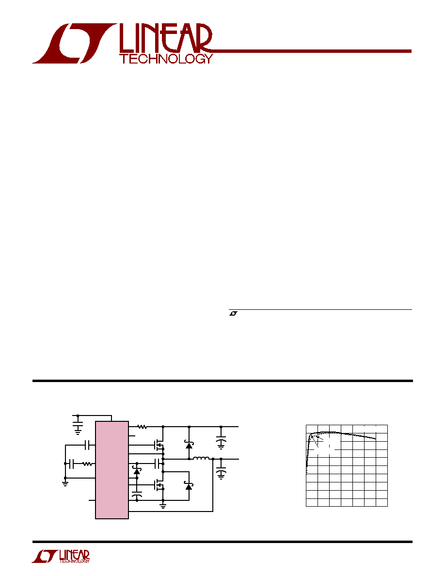
Figure 1. High Efficiency DDR Memory Termination Supply
Efficiency vs Load Current
+
D
B
CMDSH-3
D1
B320A
L1
0.68
µ
H
C
VCC
4.7
µ
F
C
IN
150
µ
F
6.3V
×
2
V
IN
2.5V TO 5.5V
V
OUT
1.25V
±
10A
+
+
C
OUT
180
µ
F
4V
×
2
M2
Si7840DP
3717 F01a
M1
Si7840DP
R
ON
715k
C
SS
0.1
µ
F
I
ON
V
REF
TG
SW
BOOST
RUN/SS
I
TH
SGND
INTV
CC
BG
PGND
V
FB
PGOOD
C
B
0.22
µ
F
R
C
20k
LTC3717
C
C
470pF
1
µ
F
V
CC
V
CC
5V TO 28V
D2
B320A
V
DD
= 2.5V
LOAD CURRENT (A)
0
EFFICIENCY (%)
3717 F01b
100
90
80
70
60
50
40
30
20
10
0
2
4
6
8
10
12
14
V
IN
= 2.5V
V
IN
= 5V
V
OUT
= 1.25V
APPLICATIO S
U
FEATURES
TYPICAL APPLICATIO
U
DESCRIPTIO
U
2
LTC3717
sn3717 3717fs
(Note 1)
Input Supply Voltage (V
CC
, I
ON
) .................36V to 0.3V
Boosted Topside Driver Supply Voltage
(BOOST) ................................................... 42V to 0.3V
SW Voltage .................................................. 36V to 5V
EXTV
CC
, (BOOST SW), RUN/SS,
PGOOD Voltages ....................................... 7V to 0.3V
V
REF
, V
RNG
Voltages ...............(INTV
CC
+ 0.3V) to 0.3V
I
TH
, V
FB
Voltages...................................... 2.7V to 0.3V
TG, BG, INTV
CC
, EXTV
CC
Peak Currents .................... 2A
TG, BG, INTV
CC
, EXTV
CC
RMS Currents .............. 50mA
Operating Ambient Temperature
Range (Note 4) ................................... 40
°
C to 85
°
C
Junction Temperature (Note 2) ............................ 125
°
C
Storage Temperature Range ................. 65
°
C to 150
°
C
Lead Temperature (Soldering, 10 sec).................. 300
°
C
ORDER PART
NUMBER
LTC3717EGN
Consult LTC Marketing for parts specified with wider operating temperature ranges.
T
JMAX
= 125
°
C,
JA
= 130
°
C/ W
The
q
denotes specifications which apply over the full operating
temperature range, otherwise specifications are T
A
= 25
°
C. V
CC
= 15V unless otherwise noted.
ABSOLUTE AXI U RATI GS
W
W
W
U
PACKAGE/ORDER I FOR ATIO
U
U
W
ELECTRICAL CHARACTERISTICS
TOP VIEW
GN PACKAGE
16-LEAD PLASTIC SSOP
1
2
3
4
5
6
7
8
16
15
14
13
12
11
10
9
RUN/SS
PGOOD
V
RNG
I
TH
SGND
I
ON
V
FB
V
REF
BOOST
TG
SW
PGND
BG
INTV
CC
V
CC
EXTV
CC
GN PART
MARKING
3717
SYMBOL
PARAMETER
CONDITIONS
MIN
TYP
MAX
UNITS
Main Control Loop
I
Q
Input DC Supply Current
Normal
1000
2000
µ
A
Shutdown Supply Current
V
RUN/SS
= 0V
15
30
µ
A
V
FB
Feedback Voltage Accuracy
I
TH
= 1.2V (Note 3), V
REF
= 2.4V
0.65
0.65
%
V
FB(LINEREG)
Feedback Voltage Line Regulation
V
CC
= 4V to 36V, I
TH
= 1.2V (Note 3)
0.002
%/V
V
FB(LOADREG)
Feedback Voltage Load Regulation
I
TH
= 0.5V to 1.9V (Note 3)
q
0.05
0.3
%
g
m(EA)
Error Amplifier Transconductance
I
TH
= 1.2V (Note 3)
0.93
1.13
1.33
mS
t
ON
On-Time
I
ON
= 30
µ
A
186
233
280
ns
I
ON
= 60
µ
A
95
115
135
ns
t
ON(MIN)
Minimum On-Time
I
ON
= 180
µ
A
50
100
ns
t
OFF(MIN)
Minimum Off-Time
I
ON
= 30
µ
A
300
400
ns
V
SENSE(MAX)
Maximum Current Sense Threshold (Source)
V
RNG
= 1V, V
FB
= V
REF/2
50mV
q
108
135
162
mV
V
PGND
V
SW
V
RNG
= 0V, V
FB
= V
REF/2
50mV
q
76
95
114
mV
V
RNG
= INTV
CC
, V
FB
= V
REF/2
50mV
q
148
185
222
mV
V
SENSE(MIN)
Minimum Current Sense Threshold (Sink)
V
RNG
= 1V, V
FB
= V
REF/2
+ 50mV
q
140
165
190
mV
V
PGND
V
SW
V
RNG
= 0V, V
FB
= V
REF/2
+ 50mV
q
97
115
133
mV
V
RNG
= INTV
CC
, V
FB
= V
REF/2
+ 50mV
q
200
235
270
mV
V
FB(OV)
Output Overvoltage Fault Threshold
8
10
12
%
V
FB(UV)
Output Undervoltage Fault Threshold
25
%
V
RUN/SS(ON)
RUN Pin Start Threshold
q
0.8
1.5
2
V
V
RUN/SS(LE)
RUN Pin Latchoff Enable Threshold
RUN/SS Pin Rising
4
4.5
V
V
RUN/SS(LT)
RUN Pin Latchoff Threshold
RUN/SS Pin Falling
3.5
4.2
V
I
RUN/SS(C)
Soft-Start Charge Current
0.5
1.2
3
µ
A
I
RUN/SS(D)
Soft-Start Discharge Current
0.8
1.8
3
µ
A
3
LTC3717
sn3717 3717fs
The
q
denotes specifications which apply over the full operating
temperature range, otherwise specifications are T
A
= 25
°
C. V
CC
= 15V unless otherwise noted.
ELECTRICAL CHARACTERISTICS
Note 1: Absolute Maximum Ratings are those values beyond which the life of
a device may be impaired.
Note 2: T
J
is calculated from the ambient temperature T
A
and power
dissipation P
D
as follows:
LTC3717EGN: T
J
= T
A
+ (P
D
· 130
°
C/W)
Note 3: The LTC3717 is tested in a feedback loop that adjusts V
FB
to achieve
a specified error amplifier output voltage (I
TH
).
Note 4: The LTC3717E is guaranteed to meet performance specifications from
0
°
C to 70
°
C. Specifications over the 40
°
C to 85
°
C operating temperature
range are assured by design, characterization and correlation with statistical
process controls.
SYMBOL
PARAMETER
CONDITIONS
MIN
TYP
MAX
UNITS
V
CC(UVLO)
Undervoltage Lockout Threshold
V
CC
Falling
q
3.4
3.9
V
V
CC(UVLOR)
Undervoltage Lockout Threshold
V
CC
Rising
q
3.5
4
V
TG R
UP
TG Driver Pull-Up On Resistance
TG High
2
3
TG R
DOWN
TG Driver Pull-Down On Resistance
TG Low
2
3
BG R
UP
BG Driver Pull-Up On Resistance
BG High
3
4
BG R
DOWN
BG Driver Pull-Down On Resistance
BG Low
1
2
TG t
r
TG Rise Time
C
LOAD
= 3300pF
20
ns
TG t
f
TG Fall Time
C
LOAD
= 3300pF
20
ns
BG t
r
BG Rise Time
C
LOAD
= 3300pF
20
ns
BG t
f
BG Fall Time
C
LOAD
= 3300pF
20
ns
Internal V
CC
Regulator
V
INTVCC
Internal V
CC
Voltage
6V < V
CC
< 30V, V
EXTVCC
= 4V
q
4.7
5
5.3
V
V
LDO(LOADREG)
Internal V
CC
Load Regulation
I
CC
= 0mA to 20mA, V
EXTVCC
= 4V
0.1
±
2
%
V
EXTVCC
EXTV
CC
Switchover Voltage
I
CC
= 20mA, V
EXTVCC
Rising
q
4.5
4.7
V
V
EXTVCC
EXTV
CC
Switch Drop Voltage
I
CC
= 20mA, V
EXTVCC
= 5V
150
300
mV
V
EXTVCC(HYS)
EXTV
CC
Switchover Hysteresis
200
mV
PGOOD Output
V
FBH
PGOOD Upper Threshold
V
FB
Rising (0% = 1/3 V
REF
)
8
10
12
%
V
FBL
PGOOD Lower Threshold
V
FB
Falling (0% = 1/3 V
REF
)
8
10
12
%
V
FB(HYS)
PGOOD Hysteresis
V
FB
Returning (0% = 1/3 V
REF
)
1
2
%
V
PGL
PGOOD Low Voltage
I
PGOOD
= 5mA
0.15
0.4
V
4
LTC3717
sn3717 3717fs
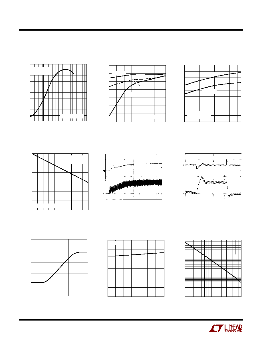
TYPICAL PERFOR A CE CHARACTERISTICS
U
W
LOAD CURRENT (A)
EFFICIENCY (%)
100
90
80
70
60
50
40
30
20
10
0
0.01
1
10
100
3717 G06
0.1
V
IN
= 2.5V
V
OUT
= 1.25V
FIGURE 1 CIRCUIT
INPUT VOLTAGE (V)
1.5
1.7
1.9
2.1
2.3
2.5
2.7
2.9
V
OUT
/V
IN
(%)
3717 G07
50.00
49.95
49.90
49.85
49.80
49.75
49.70
49.65
LOAD = 0A
LOAD = 10A
FIGURE 1 CIRCUIT
LOAD = 1A
1.5
1.7
1.9
2.1
2.3
2.5
2.7
2.9
INPUT VOLTAGE (V)
FREQUENCY (kHz)
3717 G08
450
400
350
300
250
200
150
100
50
0
LOAD = 0A
V
OUT
= 1.25V
FIGURE 1 CIRCUIT
LOAD = 10A
LOAD CURRENT (A)
0
1
2
3
4
5
6
7
8
9
10
V
OUT
/V
OUT
(%)
3717 G09
0
0.1
0.2
0.3
0.4
0.5
0.6
V
IN
= 2.5V
V
OUT
= 1.25V
FIGURE 1 CIRCUIT
Efficiency vs Load Current
V
OUT
/V
IN
Tracking Ratio vs Input
Voltage
Frequency vs Input Voltage
Load Regulation
Start-Up Response
Load-Step Transient
V
IN
= 2.5V
4ms/DIV
3718 G09.eps
V
OUT
= 1.25V
LOAD = 0.2
FIGURE 1 CIRCUIT
V
IN
= 2.5V
20
µ
s/DIV
3718 G10.eps
V
OUT
= 1.25V
LOAD = 500mA TO 10A STEP
FIGURE 1 CIRCUIT
V
OUT
1V/DIV
I
L
2A/DIV
V
OUT
200mV/DIV
I
L
5A/DIV
V
ON
VOLTAGE (V)
0
ON-TIME (ns) 400
600
3717 G11
200
0
1
2
3
1000
I
ION
= 30
µ
A
800
TEMPERATURE (
°
C)
50
ON-TIME (ns)
200
250
300
25
75
3717 G12
150
100
25
0
50
100
125
50
0
I
ION
= 30
µ
A
I
ON
CURRENT (
µ
A)
1
10
ON-TIME (ns)
100
1k
10k
10
100
3717 G13
On-Time vs V
ON
Voltage
On-Time vs
Temperature
On-Time vs I
ON
Current
5
LTC3717
sn3717 3717fs
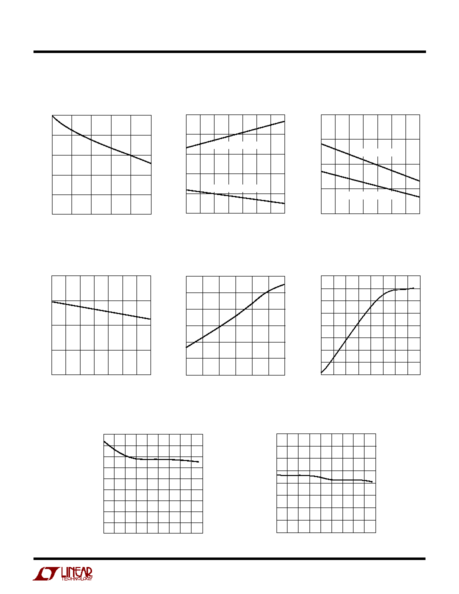
TYPICAL PERFOR A CE CHARACTERISTICS
U
W
TEMPERATURE (
°
C)
50
3.0
RUN/SS THRESHOLD (V) 3.5
4.0
4.5
5.0
25
0
25
50
3717 G16
75
100
125
LATCHOFF ENABLE
LATCHOFF THRESHOLD
TEMPERATURE (C)
50
2.0
UNDERVOLTAGE LOCKOUT THRESHOLD (V)
2.5
3.0
3.5
4.0
25
0
25
50
3717 G17
75
100
125
V
RNG
(V)
0.50
MAXIMUM CURRENT SENSE THRESHOLD (mV)
300
250
200
150
100
50
0
0.75
1.00
1.25
1.50
3717 G18
1.75
2.00
RUN/SS (V)
2.0
MAXIMUM CURRENT SENSE THRESHOLD (mV)
3.6
3717 G19
2.8
3.0
3.2
3.4
2.2
2.4
2.6
160
140
120
100
80
60
40
20
0
Maximum Current Sense Threshold
vs V
RNG
Voltage
Maximum Current Sense Threshold
vs RUN/SS Voltage, V
RNG
= 1V
RUN/SS Latchoff Thresholds
vs Temperature
Undervoltage Lockout Threshold
vs Temperature
INTV
CC
LOAD CURRENT (mA)
0
INTV
CC
(%)
0.2
0.1
0
40
3717 G14
0.3
0.4
0.5
10
20
30
50
TEMPERATURE (
°
C)
50
25
2
FCB PIN CURRENT (
µ
A)
0
3
0
50
75
3717 G15
1
2
1
25
100
125
PULL-UP CURRENT
PULL-DOWN CURRENT
INTV
CC
Load Regulation
RUN/SS Latchoff Thresholds
vs Temperature
TEMPERATURE (
°
C)
MAXIMUM CURRENT SENSE THRESHOLD (mV)
70
180
160
140
120
100
80
60
40
20
0
3717 G20
50
130
30 10 10
30
50
90 110
TEMPERATURE (
°
C)
gm (ms)
70
1.50
1.40
1.30
1.20
1.10
1.00
0.90
0.80
0.70
3717 G21
50
130
30 10 10
30
50
90 110
Error Amplifier gm
vs Temperature
Maximum Current Sense Threshold
vs Temperature, V
RNG
= 1V