 | ÐлекÑÑоннÑй компоненÑ: LTC3720 | СкаÑаÑÑ:  PDF PDF  ZIP ZIP |
Äîêóìåíòàöèÿ è îïèñàíèÿ www.docs.chipfind.ru
1
LTC3720
3720f
Single Phase VRM8.5
Current Mode Step-Down Controller
s
5-Bit Programmable Output Voltage:
1.05V to 1.825V (VRM8.5)
s
No Sense Resistor Required
s
2% to 87% Duty Cycle at 200kHz
s
t
ON(MIN)
100ns
s
Supports Active Voltage Positioning
s
True Current Mode Control
s
Stable with Ceramic C
OUT
s
Dual N-Channel MOSFET Synchronous Drive
s
Power Good Output Voltage Monitor
s
Wide V
IN
Range: 4V to 36V
s
±
1% 0.8V Reference
s
Adjustable Current Limit
s
Adjustable Switching Frequency
s
Forced Continuous Control Pin
s
Programmable Soft-Start
s
Output Overvoltage Protection
s
Optional Short-Circuit Shutdown Timer
s
Micropower Shutdown: I
Q
< 30
µ
A
s
Available in 28-Lead Narrow SSOP Package
s
Power Supplies for Pentium
®
Processors
s
Notebook Computers and Servers
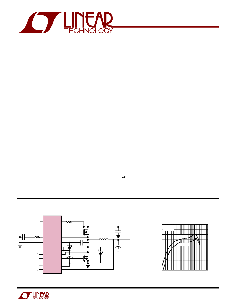
The LTC
®
3720 is a synchronous step-down switching
regulator controller for CPU power. An output voltage
between 1.05V and 1.825V is selected by a 5-bit code
(Intel VRM8.5 VID specification). The controller uses a
valley current control architecture to deliver very low duty
cycles without requiring a sense resistor. Operating fre-
quency is selected by an external resistor and is compen-
sated for variations in V
IN
and V
OUT
.
Discontinuous mode operation provides high efficiency
operation at light loads. A forced continuous control pin
reduces noise and RF interference and can assist second-
ary winding regulation by disabling discontinuous mode
operation when the main output is lightly loaded.
Fault protection is provided by internal foldback current
limiting, an output overvoltage comparator and optional
short-circuit shutdown timer. Soft-start capability for sup-
ply sequencing is accomplished using an external timing
capacitor. The regulator current limit level is also user
programmable. Wide supply range allows operation from
4V to 36V at the input.
, LTC and LT are registered trademarks of Linear Technology Corporation.
No R
SENSE
is a trademark of Linear Technology Corporation.
Pentium is a registered trademark of Intel Corporation.
CMDSH-3
UPS840
C
OUT
: CORNELL DUBILIER
ESRE271M02B
L1: SUMIDA CEP125-IROMC
L1
1
µ
H
4.7
µ
F
10
µ
F
×
5
V
IN
5V TO 24V
V
OUT
1.05V TO 1.825V
20A
+
C
OUT
270
µ
F
2V
×
4
IRF7811W
×
3
3720 F01a
IRF7811W
×
2
330k
0.1
µ
F
I
ON
PGOOD
V
IN
TG
SW
BOOST
RUN/SS
I
TH
SGND
INTV
CC
BG
PGND
5-BIT VID
V
OSENSE
VID0
VID1
VID2
VID3
VID4
0.33
µ
F
20k
LTC3720
470pF
SENSE¯
SENSE
+
V
CC
+
Figure 1. High Efficiency Step-Down Converter
OUTPUT CURRENT (A)
0.01
EFFICIENCY (%)
100
3720 F01b
0.1
1
10
100
95
90
85
80
75
70
65
60
55
V
IN
= 5V
V
IN
= 15V
V
OUT
= 1.45V
L1 = 1
µ
H
Efficiency vs Output Current
DESCRIPTIO
U
FEATURES
APPLICATIO S
U
TYPICAL APPLICATIO
U
2
LTC3720
3720f
(Note 1)
Input Supply Voltage
V
IN
, I
ON
..................................................36V to 0.3V
Boosted Topside Driver Supply Voltage
BOOST .................................................. 42V to 0.3V
SW, SENSE
+
Voltages ................................. 36V to 5V
EXTV
CC
, (BOOST SW), RUN/SS, V
CC
VID0-VID4, PGOOD Voltages ..................... 7V to 0.3V
FCB, V
ON
, V
RNG
Voltages .......... INTV
CC
+ 0.3V to 0.3V
I
TH
, V
FB
, V
OSENSE
Voltages ....................... 2.7V to 0.3V
TG, BG, INTV
CC
, EXTV
CC
Peak Currents .................... 2A
TG, BG, INTV
CC
, EXTV
CC
RMS Currents .............. 50mA
Operating Ambient Temperature Range
LTC3720EGN (Note 2) ........................ 40
°
C to 85
°
C
Junction Temperature (Note 3) ............................ 125
°
C
Storage Temperature Range ................. 65
°
C to 150
°
C
Lead Temperature (Soldering, 10 sec).................. 300
°
C
ORDER PART
NUMBER
LTC3720EGN
T
JMAX
= 125
°
C,
JA
= 95
°
C/ W
The
q
denotes specifications which apply over the full operating
temperature range, otherwise specifications are T
A
= 25
°
C. V
IN
= 15V unless otherwise noted.
ABSOLUTE AXI U RATI GS
W
W
W
U
PACKAGE/ORDER I FOR ATIO
U
U
W
ELECTRICAL CHARACTERISTICS
Consult LTC Marketing for parts specified with wider operating temperature ranges.
1
2
3
4
5
6
7
8
9
10
11
12
13
14
TOP VIEW
GN PACKAGE
28-LEAD NARROW PLASTIC SSOP
28
27
26
25
24
23
22
21
20
19
18
17
16
15
RUN/SS
V
ON
PGOOD
V
RNG
FCB
I
TH
SGND
I
ON
V
FB
SGND
V
FB
V
OSENSE
VID0
VID1
BOOST
TG
SW
SENSE
+
SENSE
PGND
BG
INTV
CC
V
IN
EXTV
CC
V
CC
VID4
VID3
VID2
SYMBOL
PARAMETER
CONDITIONS
MIN
TYP
MAX
UNITS
Main Control Loop
I
Q
Input DC Supply Current
Normal
900
2000
µ
A
Shutdown Supply Current
15
30
µ
A
V
FB
Feedback Reference Voltage
I
TH
= 1.2V (Note 4)
q
0.792
0.800
0.808
V
V
FB(LINEREG)
Feedback Voltage Line Regulation
V
IN
= 4V to 30V, I
TH
= 1.2V (Note 4)
0.002
%/V
V
FB(LOADREG)
Feedback Voltage Load Regulation
I
TH
= 0.5V to 1.9V (Note 4)
q
0.05
0.3
%
I
FB
Feedback Pin Input Current
5
±
50
nA
g
m(EA)
Error Amplifier Transconductance
I
TH
= 1.2V (Note 4)
1.4
1.7
2
mS
V
FCB
Forced Continuous Threshold
q
0.76
0.8
0.84
V
I
FCB
Forced Continuous Pin Current
V
FCB
= 0.8V
1
2
µ
A
t
ON
On-Time
I
ON
= 60
µ
A, V
ON
= 1.5V
200
250
300
ns
I
ON
= 30
µ
A, V
ON
= 1.5V
425
500
575
ns
t
ON(MIN)
Minimum On-Time
I
ON
= 180
µ
A, V
ON
= 0V
50
100
ns
t
OFF(MIN)
Minimum Off-Time
I
ON
= 60
µ
A, V
ON
= 1.5V
250
400
ns
V
SENSE(MAX)
Maximum Current Sense Threshold
V
RNG
= 1V, V
FB
= 0.76V
q
113
133
153
mV
V
SENSE
V
SENSE
+
V
RNG
= 0V, V
FB
= 0.76V
q
79
93
107
mV
V
RNG
= INTV
CC
, V
FB
= 0.76V
q
158
186
214
mV
V
SENSE(MIN)
Minimum Current Sense Threshold
V
RNG
= 1V, V
FB
= 0.84V
67
mV
V
SENSE
V
SENSE
+
V
RNG
= 0V, V
FB
= 0.84V
47
mV
V
RNG
= INTV
CC
, V
FB
= 0.84V
93
mV
V
FB(OV)
Output Overvoltage Fault Threshold
5.5
7.5
9.5
%
V
FB(UV)
Output Undervoltage Fault Threshold
520
600
680
mV
V
RUN/SS(ON)
RUN Pin Start Threshold
q
0.8
1.5
2
V
3
LTC3720
3720f
The
q
denotes specifications which apply over the full operating
temperature range, otherwise specifications are T
A
= 25
°
C. V
IN
= 15V unless otherwise noted.
ELECTRICAL CHARACTERISTICS
Note 1: Absolute Maximum Ratings are those values beyond which the life of
a device may be impaired.
Note 2: The LTC3720E is guaranteed to meet performance specifications from
0
°
C to 70
°
C. Specifications over the 40
°
C to 85
°
C operating temperature
range are assured by design, characterization and correlation with statistical
process controls.
Note 3: T
J
is calculated from the ambient temperature T
A
and power
dissipation P
D
as follows:
LTC3720EGN: T
J
= T
A
+ (P
D
· 95
°
C/W)
Note 4: The LTC3720 is tested in a feedback loop that adjusts V
FB
to achieve
a specified error amplifier output voltage (I
TH
).
Note 5: The LTC3720 VID DAC is tested in a feedback loop that adjusts
V
OSENSE
to achieve a specified feedback voltage (V
FB
= 0.8V) for each DAC VID
code.
Note 6: Each built-in pull-up resistor attached to VID inputs also has a series
diode connected to V
CC
to allow input voltages higher than the V
CC
supply
without damage or clamping. (See Operation section for further details.)
Note 7: Supply current is specified with all VID inputs floating. Due to the
internal pull-ups on the VID pins, the supply current will increase depending
on the number of grounded VID lines. Each grounded VID line will draw
approximately (V
CC
0.6V)/40k mA. (See Operation section for further
details.)
SYMBOL
PARAMETER
CONDITIONS
MIN
TYP
MAX
UNITS
V
RUN/SS(LE)
RUN Pin Latchoff Enable Threshold
RUN/SS Pin Rising
4
4.5
V
V
RUN/SS(LT)
RUN Pin Latchoff Threshold
RUN/SS Pin Falling
3.5
V
I
RUN/SS(C)
Soft-Start Charge Current
0.5
1.2
3
µ
A
I
RUN/SS(D)
Soft-Start Discharge Current
0.8
1.8
3
µ
A
V
IN
(UVLO)
Undervoltage Lockout
V
IN
Falling
q
3.4
3.9
V
V
IN
Rising
q
3.5
4.0
V
TG R
UP
TG Driver Pull-Up On Resistance
TG High
2
3
TG R
DOWN
TG Driver Pull-Down On Resistance
TG Low
2
3
BG R
UP
BG Driver Pull-Up On Resistance
BG High
3
4
BG R
DOWN
BG Driver Pull-Down On Resistance
BG Low
1
2
TG t
r
TG Rise Time
C
LOAD
= 3300pF
20
ns
TG t
f
TG Fall Time
C
LOAD
= 3300pF
20
ns
BG t
r
BG Rise Time
C
LOAD
= 3300pF
20
ns
BG t
f
BG Fall Time
C
LOAD
= 3300pF
20
ns
Internal V
CC
Regulator
V
INTVCC
Internal V
CC
Voltage
6V < V
IN
< 30V, V
EXTVCC
= 4V
q
4.7
5
5.3
V
V
LDO(LOADREG)
Internal V
CC
Load Regulation
I
CC
= 0mA to 20mA, V
EXTVCC
= 4V
0.1
±
2
%
V
EXTVCC
EXTV
CC
Switchover Voltage
I
CC
= 20mA, V
EXTVCC
Rising
q
4.5
4.7
V
V
EXTVCC
EXTV
CC
Switch Drop Voltage
I
CC
= 20mA, V
EXTVCC
= 5V
150
300
mV
V
EXTVCC(HYS)
EXTV
CC
Switchover Hysteresis
200
mV
PGOOD Output
V
FBH
PGOOD Upper Threshold
V
FB
Rising
5.5
7.5
9.5
%
V
FBL
PGOOD Lower Threshold
V
FB
Falling
5.5
7.5
9.5
%
V
FB(HYS)
PGOOD Hysteresis
V
FB
Returning
1
2
%
V
PGL
PGOOD Low Voltage
I
PGOOD
= 5mA
0.15
0.4
V
VID DAC
V
CC
Operating Supply Voltage Range
3.1
5.5
V
V
VID(T)
VID0-VID4 Logic Threshold Voltage
V
CC
= 3.3V
0.4
1.2
2
V
V
VID(LEAK)
VID0-VID4 Leakage Current
V
VID0
-V
VID4
= V
CC
0.01
±
1
µ
A
V
OSENSE
DAC Output Accuracy
V
OSENSE
Programmed from
0.25
0
0.25
%
1.05V to 1.825V (Note 5), V
CC
= 5V
R
PULLUP
Pull-Up Resistance on VID
V
DIODE
= 0.6V (Note 6)
28
40
56
k
R
VID
Resistance from V
OSENSE
to V
FB
6
10
14
k
I
VCC
Supply Current
(Note 7)
1
10
µ
A
4
LTC3720
3720f
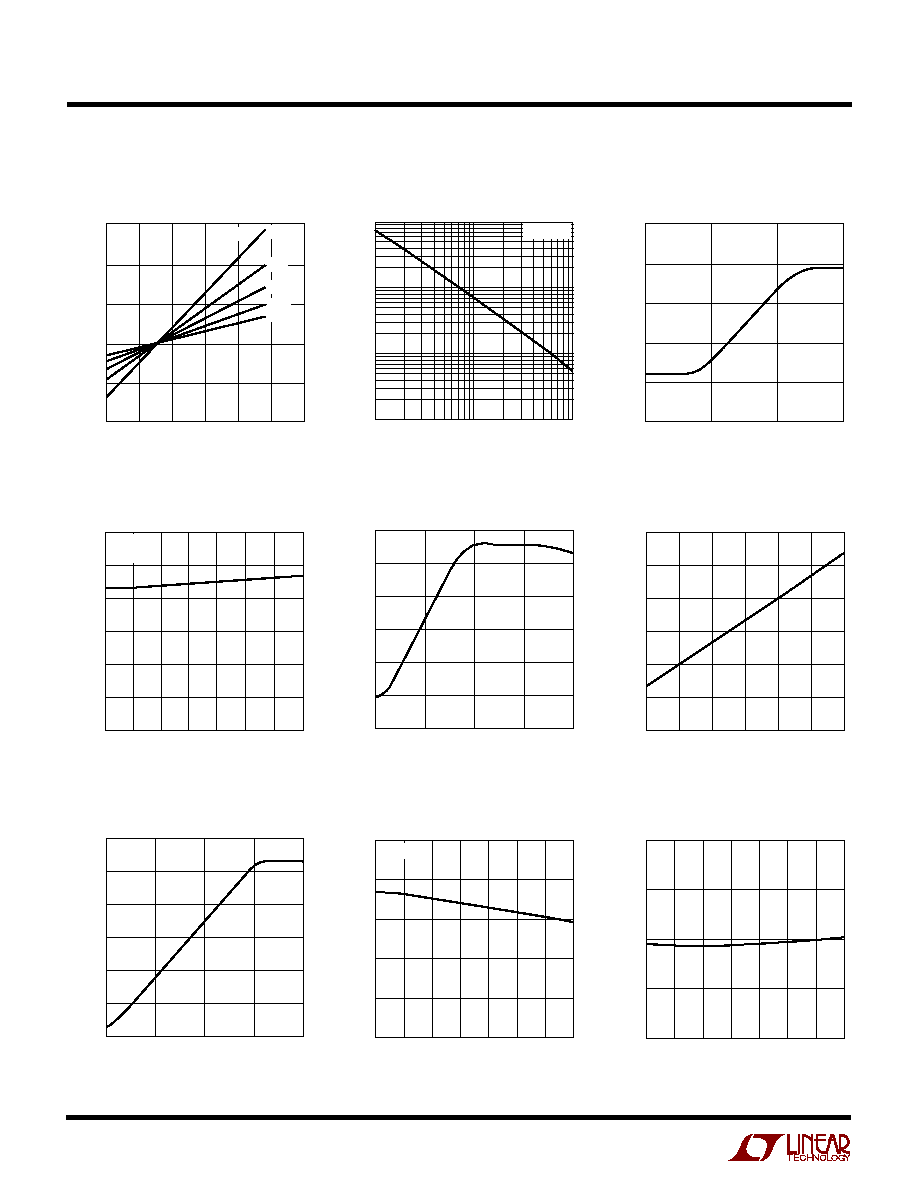
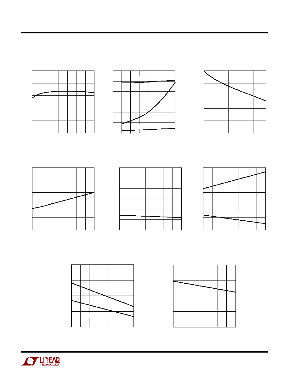
TYPICAL PERFOR A CE CHARACTERISTICS
U
W
Current Sense Threshold
vs I
TH
Voltage
I
TH
VOLTAGE (V)
0
200
CURRENT SENSE THRESHOLD (mV)
100
0
100
200
300
0.5
1.0
1.5
2.0
3720 G01
2.5
3.0
V
RNG
=
1V
0.7V
0.5V
1.4V
2V
I
ON
CURRENT (
µ
A)
1
10
ON-TIME (ns)
100
1k
10k
10
100
3720 G02
V
VON
= 0V
V
ON
VOLTAGE (V)
0
ON-TIME (ns) 400
600
3720 G02
200
0
1
2
3
1000
I
ION
= 30
µ
A
800
On-Time vs I
ON
Current
On-Time vs V
ON
Voltage
On-Time vs Temperature
TEMPERATURE (
°
C)
50
ON-TIME (ns)
200
250
300
25
75
3720 G04
150
100
25
0
50
100
125
50
0
I
ION
= 30
µ
A
V
VON
= 0V
V
FB
(V)
0
0
MAXIMUM CURRENT SENSE THRESHOLD (mV)
25
50
75
100
125
150
V
RNG
= 1V
0.2
0.4
0.6
0.8
3720 G05
Current Limit Foldback
V
RNG
VOLTAGE (V)
0.5
0
MAXIMUM CURRENT SENSE THRESHOLD (mV)
50
100
150
200
300
0.75
1.0
1.25
1.5
3720 G06
1.75
2.0
250
Maximum Current Sense
Threshold vs V
RNG
Voltage
Maximum Current Sense
Threshold vs RUN/SS Voltage
RUN/SS VOLTAGE (V)
1.5
0
MAXIMUM CURRENT SENSE THRESHOLD (mV)
25
50
75
100
125
150
V
RNG
= 1V
2
2.5
3
3.5
3729 G07
Maximum Current Sense
Threshold vs Temperature
TEMPERATURE (
°
C)
50
25
100
MAXIMUM CURRENT SENSE THRESHOLD (mV)
120
150
0
50
75
3720 G08
110
140
130
25
100
125
V
RNG
= 1V
TEMPERATURE (
°
C)
50
0.78
FEEDBACK REFERENCE VOLTAGE (V)
0.79
0.80
0.81
0.82
25
0
25
50
3720 G09
75
100
125
Feedback Reference Voltage
vs Temperature
5
LTC3720
3720f
TYPICAL PERFOR A CE CHARACTERISTICS
U
W
Error Amplifier g
m
vs Temperature
EXTV
CC
Switch Resistance
vs Temperature
RUN/SS Latchoff Thresholds
vs Temperature
TEMPERATURE (
°
C)
50
25
1.0
g
m
(mS)
1.4
2.0
0
50
75
3720 G10
1.2
1.8
1.6
25
100
125
INPUT VOLTAGE (V)
0
INPUT CURRENT (
µ
A)
SHUTDOWN CURRENT (
µ
A)
800
1000
1200
15
25
3720 G11
600
400
5
10
20
30
35
200
0
30
40
60
50
20
10
0
EXTV
CC
OPEN
EXTV
CC
= 5V
SHUTDOWN
INTV
CC
LOAD CURRENT (mA)
0
INTV
CC
(%)
0.2
0.1
0
40
3720 G12
0.3
0.4
0.5
10
20
30
50
Input and Shutdown Currents
vs Input Voltage
INTV
CC
Load Regulation
TEMPERATURE (
°
C)
50
25
0
EXTV
CC
SWITCH RESISTANCE (
)
4
10
0
50
75
3720 G13
2
8
6
25
100
125
TEMPERATURE (
°
C)
50
FCB PIN CURRENT (
µ
A)
0.50
0.25
0
25
75
3720 G14
0.75
1.00
25
0
50
100
125
1.25
1.50
TEMPERATURE (
°
C)
50
25
2
FCB PIN CURRENT (
µ
A)
0
3
0
50
75
3720 G15
1
2
1
25
100
125
PULL-UP CURRENT
PULL-DOWN CURRENT
FCB Pin Current vs Temperature
RUN/SS Pin Current
vs Temperature
TEMPERATURE (
°
C)
50
3.0
RUN/SS THRESHOLD (V) 3.5
4.0
4.5
5.0
25
0
25
50
3720 G16
75
100
125
LATCHOFF ENABLE
LATCHOFF THRESHOLD
TEMPERATURE (C)
50
2.0
UNDERVOLTAGE LOCKOUT THRESHOLD (V)
2.5
3.0
3.5
4.0
25
0
25
50
3720 G17
75
100
125
Undervoltage Lockout Threshold
vs Temperature