 | –≠–ª–µ–∫—Ç—Ä–æ–Ω–Ω—ã–π –∫–æ–º–ø–æ–Ω–µ–Ω—Ç: LTC3776 | –°–∫–∞—á–∞—Ç—å:  PDF PDF  ZIP ZIP |
1
LTC3776
3776f
, LTC and LT are registered trademarks of Linear Technology Corporation. Burst Mode
is a registered trademark of Linear Technology Corporation.
No R
SENSE
is a trademark of
Linear Technology Corporation.
All other trademarks are the property of their respective
owners. Protected by U.S. Patents including
5481178, 5929620, 6144194, 6580258,
6304066, 6611131, 6498466, patent pending on Spread Spectrum.
Dual 2-Phase, No R
SENSE
TM
,
Synchronous Controller for
DDR/QDR Memory Termination
High Efficiency, 2-Phase, DDR Memory (V
DDQ
and V
TT
) Supplies
No Current Sense Resistors Required
Out-of-Phase Controllers Reduce Required
Input Capacitance
V
OUT2
Tracks 1/2 V
REF
Symmetrical Source/Sink Output Current
Capability (V
OUT2
)
Spread Spectrum Operation (When Enabled)
Wide V
IN
Range: 2.75V to 9.8V
Constant Frequency Current Mode Operation
0.6V ±1.5% Voltage Reference (V
OUT1
)
Low Dropout Operation: 100% Duty Cycle
True PLL for Frequency Locking or Adjustment
Internal Soft-Start Circuitry
Power Good Output Voltage Monitor
Output Overvoltage Protection
Micropower Shutdown: I
Q
= 9µA
Tiny Low Profile (4mm ◊ 4mm) QFN and Narrow
SSOP Packages
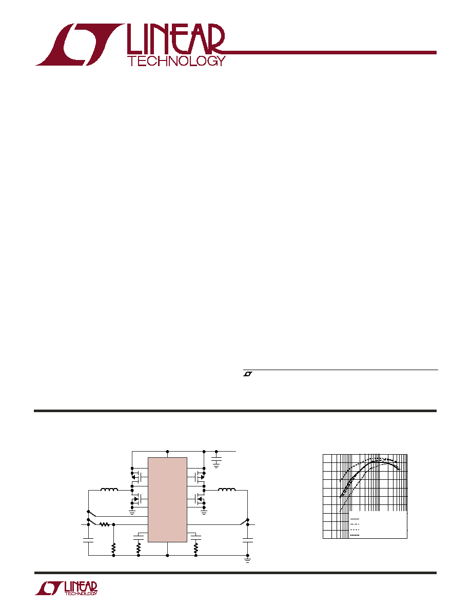
The LTC
Æ
3776 is a 2-phase dual output synchronous step-
down switching regulator controller for DDR/QDR memory
termination applications. The second controller regulates
its output voltage to 1/2 V
REF
while providing symmetrical
source and sink output current capability.
The No R
SENSE
constant frequency current mode architec-
ture eliminates the need for sense resistors and improves
efficiency. Power loss and noise due to the ESR of the
input capacitance are minimized by operating the two
controllers out of phase.
The switching frequency can be programmed up to 750kHz,
allowing the use of small surface mount inductors and ca-
pacitors. For noise sensitive applications, the LTC3776
switching frequency can be externally synchronized from
250kHz to 850kHz, or can be enabled for spread spectrum
operation. Forced continuous operation reduces noise and
RF interference. Soft-start for V
OUT1
is provided internally
and can be extended using an external capacitor.
The LTC3776 is available in the tiny thermally enhanced
(4mm ◊ 4mm) QFN package or 24-lead SSOP narrow
package.
DDR, DDR II and QDR Memory
SSTL, HSTL Termination Supplies
Servers, RAID Systems
Distributed DC Power Systems
SENSE1
+
V
IN
LTC3776
SGND
SENSE2
+
TG1
TG2
SW1
SW2
BG1
BG2
PGND
PGND
V
REF
V
FB2
470pF
(V
DDQ
)V
OUT1
2.5V
4A
V
OUT2
(V
TT
)
1.25V
±4A
47µF
47µF
15k
2200pF
6.2k
59k
187k
1.5µH
1.5µH
I
TH1
3776 TA01a
I
TH2
10µF
◊2
V
IN
3.3V
V
FB1
LOAD CURRENT (mA)
EFFICIENCY (%)
100
60
90
80
70
10
100
1000
10000
3776 TA01b
0
50
40
30
20
10
FIGURE 14 CIRCUIT
CHANNEL 2 (V
IN
= 3.3V)
CHANNEL 1 (V
IN
= 5V)
CHANNEL 1 (V
IN
= 3.3V)
CHANNEL 2 (V
IN
= 5V)
Efficiency vs Load Current
FEATURES
DESCRIPTIO
U
APPLICATIO S
U
TYPICAL APPLICATIO
U

2
LTC3776
3776f
Input Supply Voltage (V
IN
) ........................ ≠ 0.3V to 10V
PLLLPF, RUN/SS, SYNC/SSEN,
V
REF
, SENSE1
+
, SENSE2
+
, V
FB2
IPRG1, IPRG2 Voltages ................. ≠ 0.3V to (V
IN
+ 0.3V)
V
FB1
, I
TH1
, I
TH2
Voltages ........................... ≠ 0.3V to 2.4V
SW1, SW2 Voltages .............. ≠2V to V
IN
+ 1V (10V Max)
PGOOD ..................................................... ≠ 0.3V to 10V
ABSOLUTE AXI U RATI GS
W
W
W
U
(Note 1)
TG1, TG2, BG1, BG2 Peak Output Current (<10µs) ..... 1A
Operating Temperature Range (Note 2) ... ≠40∞C to 85∞C
Storage Temperature Range .................. ≠65∞C to 125∞C
Junction Temperature (Note 3) ............................ 125∞C
Lead Temperature (Soldering, 10 sec)
(LTC3776EGN) ..................................................... 300∞C
PACKAGE/ORDER I FOR ATIO
U
U
W
24 23 22 21 20 19
7
8
9
TOP VIEW
25
UF PACKAGE
24-LEAD (4mm ◊ 4mm) PLASTIC QFN
10 11 12
6
5
4
3
2
1
13
14
15
16
17
18
I
TH1
IPRG2
PLLLPF
SGND
V
IN
V
REF
SYNC/SSEN
TG1
PGND
TG2
RUN/SS
BG2
V
FB1
IPRG1
SW1
SENSE1
+
PGND
BG1
V
FB2
I
TH2
PGOOD
SW2
SENSE2
+
PGND
T
JMAX
= 125∞C,
JA
= 37∞C/W
EXPOSED PAD (PIN 25) IS PGND
MUST BE SOLDERED TO PCB
1
2
3
4
5
6
7
8
9
10
11
12
TOP VIEW
GN PACKAGE
24-LEAD PLASTIC SSOP
24
23
22
21
20
19
18
17
16
15
14
13
SW1
IPRG1
V
FB1
I
TH1
IPRG2
PLLLPF
SGND
V
IN
V
REF
V
FB2
I
TH2
PGOOD
SENSE1
+
PGND
BG1
SYNC/SSEN
TG1
PGND
TG2
RUN/SS
BG2
PGND
SENSE2
+
SW2
ORDER PART
NUMBER
UF PART MARKING
3776
LTC3776EUF
T
JMAX
= 125∞C,
JA
= 130∞C/ W
ORDER PART
NUMBER
LTC3776EGN
Consult LTC Marketing for parts specified with wider operating temperature ranges.
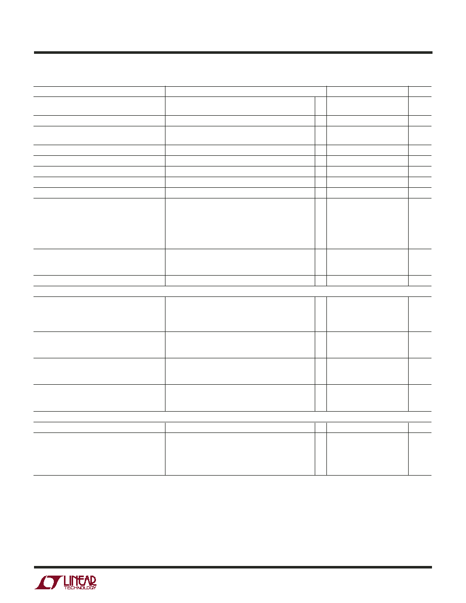
ELECTRICAL CHARACTERISTICS
The
denotes specifications that apply over the full operating temperature
range, otherwise specifications are at T
A
= 25∞C. V
IN
= 4.2V unless otherwise specified.
PARAMETER
CONDITIONS
MIN
TYP
MAX
UNITS
Main Control Loops
Input DC Supply Current
(Note 4)
Normal Operation
I
TH1
= I
TH2
= 1.3V
575
850
µA
Shutdown
RUN/SS = 0V
9
20
µA
UVLO
V
IN
< UVLO Threshold ≠200mV
3
10
µA
Undervoltage Lockout Threshold
V
IN
Falling
1.95
2.25
2.55
V
V
IN
Rising
2.15
2.45
2.75
V
Shutdown Threshold at RUN/SS
0.45
0.65
0.85
V
Start-Up Current Source
RUN/SS = 0V
0.4
0.7
1
µA
Regulated Feedback Voltage (V
FB1
)
0∞C to 85∞C (Note 5)
0.591
0.6
0.609
V
≠40∞C to 85∞C
0.588
0.6
0.612
V
Regulated Feedback Voltage (V
FB2
)
V
REF
= 2.5V
1.232
1.250
1.268
V
Output Voltage Line Regulation (V
FB1
)
2.75V < V
IN
< 9.8V (Note 5)
0.05
0.2
mV/V
Output Voltage Line Regulation (V
FB2
)
0.02
0.1
mV/V
3
LTC3776
3776f
ELECTRICAL CHARACTERISTICS
The
denotes specifications that apply over the full operating temperature
range, otherwise specifications are at T
A
= 25∞C. V
IN
= 4.2V unless otherwise specified.
Note 1: Absolute Maximum Ratings are those values beyond which the life
of a device may be impaired.
Note 2: The LTC3776E is guaranteed to meet specified performance from
0∞C to 70∞C. Specifications over the ≠40∞C to 85∞C operating range are
assured by design, characterization and correlation with statistical process
controls.
Note 3: T
J
is calculated from the ambient temperature T
A
and power
dissipation P
D
according to the following formula:
T
J
= T
A
+ (P
D
∑
JA
∞C/W)
Note 4: Dynamic supply current is higher due to gate charge being
delivered at the switching frequency.
Note 5: The LTC3776 is tested in a feedback loop that servos I
TH
to a
specified voltage and measures the resultant V
FB
voltage.
Note 6: Peak current sense voltage is reduced dependent on duty cycle to
a percentage of value as shown in Figure 2.
PARAMETER
CONDITIONS
MIN
TYP
MAX
UNITS
Output Voltage Load Regulation
I
TH
= 0.9V (Note 5)
0.12
0.5
%
I
TH
= 1.7V
≠0.12
≠0.5
%
V
FB1
Input Current
(Note 5)
10
50
nA
Overvoltage Protect Threshold
Measured at V
FB
with Respect to
10
13.3
16
%
Regulated Feedback Voltage
Overvoltage Protect Hysteresis
3
%
Top Gate (TG) Drive 1, 2 Rise Time
C
L
= 3000pF
40
ns
Top Gate (TG) Drive 1, 2 Fall Time
C
L
= 3000pF
40
ns
Bottom Gate (BG) Drive 1, 2 Rise Time
C
L
= 3000pF
50
ns
Bottom Gate (BG) Drive 1, 2 Fall Time
C
L
= 3000pF
40
ns
Maximum Current Sense Voltage (Channel 1)
IPRG1 = Floating (Note 6)
110
125
140
mV
(SENSE1
+
≠ SW1)(V
SENSE(MAX)
) (SOURCE)
IPRG1 = 0V
70
85
100
mV
IPRG1 = V
IN
185
204
223
mV
Maximum Current Sense Voltage (Channel 2)
IPRG2 = Floating (Note 6)
127
147
167
mV
(SENSE2
+
≠ SW2)(V
SENSE(MAX)
) (SOURCE)
IPRG2 = 0V
85
100
105
mV
IPRG2 = V
IN
215
245
275
mV
Minimum Current Sense Voltage (Channel 2 Only)
IPRG2 = Floating (Note 6)
≠130
≠112
≠94
mV
(SENSE2
+
≠ SW2)(V
SENSE(MAX)
) (SINK)
IPRG2 = 0V
≠90
≠75
≠60
mV
IPRG2 = V
IN
≠208
≠188
≠168
mV
Soft-Start Time
Time for V
FB1
to Ramp from 0.05V to 0.55V
0.667
0.833
1
ms
Oscillator and Phase-Locked Loop
Oscillator Frequency
Spread Spectrum Disabled (SYNC/SSEN = GND)
PLLLPF = Floating
460
550
610
kHz
PLLLPF = 0V
260
300
340
kHz
PLLLPF = V
IN
650
750
825
kHz
Spread Spectrum Frequency Range
SYNC/SSEN = V
IN
Minimum Switching Frequency
450
kHz
Maximum Switching Frequency
580
kHz
Phase-Locked Loop Lock Range
SYNC/SSEN Clocked
Minimum Synchronizable Frequency
200
250
kHz
Maximum Synchronizable Frequency
850
1150
kHz
Phase Detector Output Current
Sinking
f
OSC
> f
SYNC/FCB
≠4
µA
Sourcing
f
OSC
< f
SYNC/FCB
4
µA
PGOOD Output
PGOOD Voltage Low
I
PGOOD
Sinking 1mA
125
mV
PGOOD Trip Level
V
FB
with Respect to Set Output Voltage
V
FB
< Regulated Feedback Voltage, Ramping Positive
≠13
≠10.0
≠7
%
V
FB
< Regulated Feedback Voltage, Ramping Negative
≠16
≠13.3
≠10
%
V
FB
> Regulated Feedback Voltage, Ramping Negative
7
10.0
13
%
V
FB
> Regulated Feedback Voltage, Ramping Positive
10
13.3
16
%

4
LTC3776
3776f
TYPICAL PERFOR A CE CHARACTERISTICS
U
W
Efficiency vs Load Current
Step from Sinking to Sourcing
Load Current (CH2)
Load Step (Load Connected
Between V
OUT1
and V
OUT2
)
Tracking Start-Up with Internal
Soft-Start (C
SS
= 0µF)
Oscillator Frequency
vs Input Voltage
Tracking Start-Up with External
Soft-Start (C
SS
= 0.15µF)
T
A
= 25∞C unless otherwise noted.
Maximum Current Sense Voltage
vs I
TH1
Pin Voltage (CH1)
LOAD CURRENT (mA)
EFFICIENCY (%)
100
60
90
80
70
10
100
1000
10000
3776 G01
0
50
40
30
20
10
FIGURE 14 CIRCUIT
CHANNEL 2 (V
IN
= 3.3V)
CHANNEL 1 (V
IN
= 5V)
CHANNEL 1 (V
IN
= 3.3V)
CHANNEL 2 (V
IN
= 5V)
V
IN
= 3.3V
FIGURE 14 CIRCUIT
20µs/DIV
3776 G02
V
OUT2
100mV/DIV
AC-COUPLED
LOAD CURRENT
500mA/DIV
V
IN
= 3.3V
FIGURE 14 CIRCUIT
V
OUT1
SOURCING
V
OUT2
SINKING
20µs/DIV
3776 G03
V
OUT1
100mV/DIV
AC-COUPLED
V
OUT2
100mV/DIV
AC-COUPLED
LOAD CURRENT
1A/DIV
V
IN
= 3.3V
FIGURE 14 CIRCUIT
4ms/DIV
3776 G05
V
OUT1
=
2.5V
V
OUT2
=
1.25V
500mV/DIV
INPUT VOLTAGE (V)
2
≠5
NORMALIZED FREQUENCY SHIFT (%)
≠4
≠2
≠1
0
5
2
4
6
7
3736 G06
≠3
3
4
1
3
5
8
9
10
I
TH
VOLTAGE (V)
0.5
≠20
CURRENT LIMIT (%)
0
20
40
60
100
1
1.5
3776 G07
2
80
V
IN
= 3.3V
FIGURE 14 CIRCUIT
500µs/DIV
3776 G04
V
OUT1
=
2.5V
V
OUT2
=
1.25V
500mV/DIV
5
LTC3776
3776f
Regulated Feedback Voltage
(CH2) vs Temperature
Regulated Feedback Voltage
(CH1) vs Temperature
Shutdown (RUN) Threshold
vs Temperature
RUN/SS Pull-Up Current
vs Temperature
Maximum Current Sense Threshold
(CH1) vs Temperature
Oscillator Frequency
vs Temperature
TEMPERATURE (∞C)
≠60
≠10
NROMALIZED FREQUENCY (%)
≠8
≠4
≠2
0
10
4
≠20
20
40
3736 G15
≠6
6
8
2
≠40
0
60
80
100
TEMPERATURE (∞C)
≠60
INPUT (V
IN
) VOLTAGE (V) 2.30
2.40
100
3736 G16
2.20
2.10
≠20
20
60
≠40
0
40
80
2.50
2.25
2.35
2.15
2.45
V
IN
RISING
V
IN
FALLING
Undervoltage Lockout Threshold
vs Temperature
TYPICAL PERFOR A CE CHARACTERISTICS
U
W
T
A
= 25∞C unless otherwise noted.
Maximum Current Sense Voltage
vs I
TH2
Pin Voltage (CH2)
I
TH2
VOLTAGE (V)
0
≠100
CURRENT LIMIT (%)
≠80
≠40
≠20
0
100
40
1.5
3776 G08
≠60
60
80
20
1.0
2.0
TEMPERATURE (∞C)
≠60
FEEDBACK VOLTAGE (V
FB2
) (V)
1.2625
1.2600
1.2575
1.2550
1.2525
1.2500
1.2475
1.2450
1.2425
1.2400
1.2375
≠20
20
40
3776 G09
≠40
0
60
80
100
V
REF
= 2.500V
TEMPERATURE (∞C)
≠60
0.588
FEEDBACK VOLTAGE (V
FB1
) (V)
0.592
0.596
0.600
0.604
≠20
20
60
100
3776 G10
0.608
0.612
≠40
0
40
80
TEMPERATURE (∞C)
≠60
0
RUN/SS VOLTAGE (V)
0.1
0.3
0.4
0.5
1.0
0.7
≠20
20
40
3736 G11
0.2
0.8
0.9
0.6
≠40
0
60
80
100
TEMPERATURE (∞C)
≠60
0.4
RUN/SS PULL-UP CURRENT (
µ
A)
0.5
0.6
0.7
0.8
≠20
20
60
100
3736 G12
0.9
1.0
≠40
0
40
80
TEMPERATURE (∞C)
≠60
115
MAXIMUM CURRENT SENSE THRESHOLD (mV)
120
125
130
135
≠40 ≠20
0
20
3736 G13
40
60
80
100
I
PRG1
= FLOAT
Maximum Current Sense
Threshold (CH2) vs Temperature
TEMPERATURE (∞C)
≠60
MAXIMUM CURRENT SENSE THRESHOLD (mV)
140
145
150
0
40
100
3776 G14
135
130
125
≠40 ≠20
20
60
80
I
PRG2
= FLOAT

6
LTC3776
3776f
U
U
U
PI FU CTIO S
I
TH1
/I
TH2
(Pins 1, 8/ Pins 4, 11): Current Threshold and
Error Amplifier Compensation Point. Nominal operating
range on these pins is from 0.7V to 2V. The voltage on
these pins determines the threshold of the main current
comparator.
PLLLPF (Pin 3/Pin 6): Frequency Set/PLL Lowpass Filter.
When synchronizing to an external clock, this pin serves
as the lowpass filter point for the phase-locked loop. Nor-
mally a series RC is connected between this pin and ground.
When SYNC/SSEN is tied to GND, this pin serves as the fre-
quency select input. Tying this pin to GND selects 300kHz
operation; tying this pin to V
IN
selects 750kHz operation.
Floating this pin selects 550kHz operation. When SYNC/
SSEN is tied to V
IN
to enable spread spectrum operation,
a capacitor (1nF to 4.7nF) should be connected from this
pin to SGND to filter and smooth the changes in frequency
of the LTC3776's internal oscillator.
SGND (Pin 4/Pin 7): Small-Signal Ground. This pin serves
as the ground connection for most internal circuits.
V
IN
(Pin 5/Pin 8): Chip Signal Power Supply. This pin
powers the entire chip except for the gate drivers. Externally
filtering this pin with a lowpass RC network (e.g.,
R = 10, C = 1µF) is suggested to minimize noise pickup,
especially in high load current applications.
V
REF
(Pin 6/Pin 9): Reference voltage input for channel 2.
(UF/GN Package)
The positive input of the error amplifier for channel 2 senses
one half of the voltage on this pin through an internal
resistor divider.
PGOOD (Pin 9/Pin 12): Power Good Output Voltage Moni-
tor Open-Drain Logic Output. This pin is pulled to ground
when the voltage on either feedback pin (V
FB1
, V
FB2
) is not
within ±13.3% of its nominal set point.
PGND (Pins 12, 16, 20, 25/ Pins 15, 19, 23): Power
Ground. These pins serve as the ground connection for the
gate drivers and the negative input to the reverse current
comparators. The Exposed Pad (UF package) must be
soldered to PCB ground.
RUN/SS (Pin 14/Pin 17): Run Control Input and Optional
External Soft-Start Input. Forcing this pin below 0.65V shuts
down the chip (both channels). Driving this pin to V
IN
or
releasing this pin enables the chip, using the chip's inter-
nal soft-start. An external soft-start can be programmed by
connecting a capacitor between this pin and ground.
TG1/TG2 (Pins 17, 15/Pins 20, 18): Top (PMOS) Gate Drive
Output. These pins drive the gates of the external P-channel
MOSFETs. These pins have an output swing from PGND to
SENSE
+
.
SYNC/SSEN (Pin 18/Pin 21): Synchronization Input and
Spread Spectrum Modulation Enable Input. To synchronize
the LTC3776's switching frequency to an external clock
Shutdown Quiescent Current
vs Input Voltage
INPUT VOLTAGE (V)
2
0
SHUTDOWN CURRENT (
µ
A)
2
6
8
10
20
14
4
6
7
3736 G17
4
16
18
12
3
5
8
9
10
RUN/SS = 0V
RUN/SS Start-Up Current
vs Input Voltage
INPUT VOLTAGE (V)
2
RUN/SS PIN PULL-UP CURRENT (
µ
A)
0.5
0.6
0.7
10
3736 G18
0.4
0.3
0
0.1
4
6
8
3
5
7
9
0.2
0.9
0.8
RUN/SS = 0V
TYPICAL PERFOR A CE CHARACTERISTICS
U
W
T
A
= 25∞C unless otherwise noted.

7
LTC3776
3776f
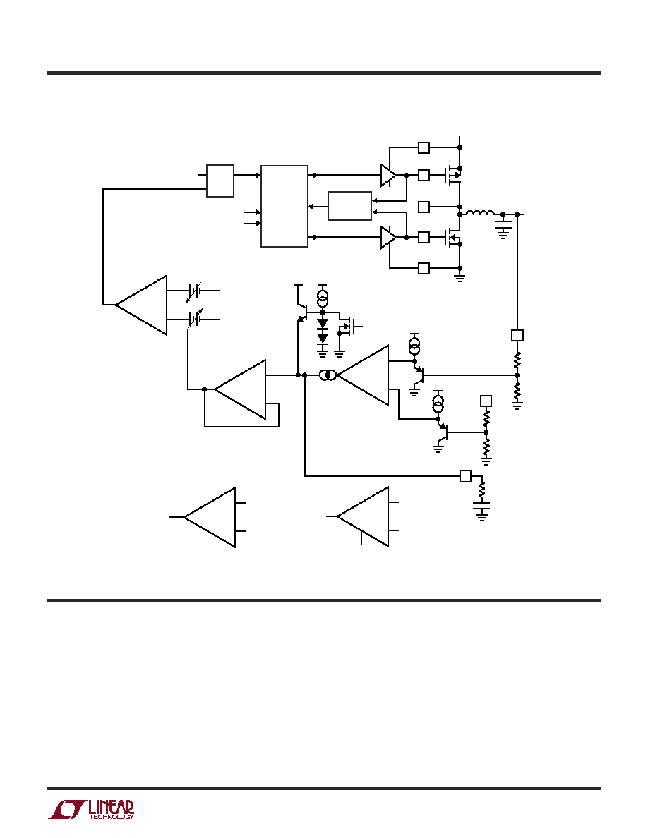
FU CTIO AL DIAGRA
U
U
W
≠
+
≠
+
≠
+
SHDN
0.6V
V
REF
EXTSS
0.7µA
CLK1
CLK2
0.54V
0.9 ∑ V
REF
/2
V
FB1
V
FB2
SLOPE1
SLOPE2
RUN/SS
V
IN
C
VIN
V
IN
(TO CONTROLLER 1, 2)
R
VIN
SYNC/SSEN
PLLLPF
UNDERVOLTAGE
LOCKOUT
SYNC DETECT/
SPREAD
SPECTRUM
ENABLE
VOLTAGE
CONTROLLED
OSCILLATOR
SLOPE
COMP
VOLTAGE
REFERENCE
t
SEC
= 1ms
INTSS
PHASE
DETECTOR
IPROG1
IPROG2
IPRG1
IPRG2
VOLTAGE
CONTROLLED
OSCILLATOR
MAXIMUM
SENSE VOLTAGE
SELECT
PGOOD
SHDN
OV1
UV1
UV2
OV2
3776 FD
(Common Circuitry)
using the phase-locked loop, apply a CMOS compatible
clock with a frequency between 250kHz and 850kHz to this
pin. Tie this pin to GND to enable constant frequency
operation (300kHz, 550kHz or 750kHz as determined by the
state of the PLLLPF pin). Tie this pin to V
IN
to enable spread
spectrum operation. In spread spectrum mode, the
LTC3776's frequency is randomly varied between 450kHz
and 580kHz.
BG1/BG2 (Pins 19, 13/Pins 22, 16): Bottom (NMOS) Gate
Drive Output. These pins drive the gates of the external N-
channel MOSFETs. These pins have an output swing from
PGND to SENSE
+
.
SENSE1
+
/SENSE2
+
(Pins 21, 11/Pins 24, 14): Positive
Input to Differential Current Comparator. Also powers the
gate drivers. Normally connected to the source of the ex-
ternal P-channel MOSFET.
SW1/SW2 (Pins 22, 10/Pins 1, 13): Switch Node Connec-
tion to Inductor. Also the negative input to differential peak
current comparator and an input to the reverse current
comparator. Normally connected to the drain of the exter-
nal P-channel MOSFETs, the drain of the external N-channel
MOSFET and the inductor.
IPRG1/IPRG2 (Pins 23, 2/Pins 2, 5): Three-State Pins to
Select Maximum Peak Sense Voltage Threshold. These pins
select the maximum allowed voltage drop between the
SENSE
+
and SW pins (i.e., the maximum allowed drop
across the external P-channel MOSFET) for each channel.
Tie to V
IN
, GND or float to select one of three discrete
levels.
V
FB1
/V
FB2
(Pins 24, 7/Pins 3, 10): Feedback Pins. Receives
the remotely sensed feedback voltage for its controller.
Exposed Pad (Pin 25/NA): The Exposed Pad (UF Package)
must be soldered to the PCB ground.
U
U
U
PI FU CTIO S
(UF/GN Package)

8
LTC3776
3776f
FU CTIO AL DIAGRA
U
U
W
Q
OV1
CLK1
SC1
SLOPE1
SW1
SENSE1
+
S
R
RS1
ANTISHOOT
THROUGH
PGND
TG1
SENSE1
+
V
IN
V
OUT1
C
IN
C
OUT1
MP1
MN1
BG1
R1B
L1
PGND
V
FB1
I
TH1
R
ITH1
C
ITH1
0.6V
0.12V
SC1
V
FB1
SW1
SENSE1
+
R1A
≠
+
EXTSS
INTSS
EAMP
SHDN
≠
+
IPROG1
≠
+
ICMP
≠
+
V
FB1
OV1
0.68V
≠
+
SWITCHING
LOGIC
AND
BLANKING
CIRCUIT
SCP
OVP
(Controller 1)
9
LTC3776
3776f
OPERATIO
U
(Refer to Functional Diagram)
Main Control Loop
The LTC3776 uses a constant frequency, current mode
architecture with the two controllers operating 180 de-
grees out of phase. During normal operation, the top
external P-channel power MOSFET is turned on when the
clock for that channel sets the RS latch, and turned off
when the current comparator (I
CMP
) resets the latch. The
FU CTIO AL DIAGRA
U
U
W
(Controller 2)
Q
OV2
CLK2
SC2
SLOPE2
SW2
SENSE2
+
SHDN
S
R
RS2
ANTISHOOT
THROUGH
PGND
SENSE2
+
TG2
SENSE2
+
V
IN
V
OUT2
C
OUT2
MP2
MN2
BG2
40k
120k
40k
L2
PGND
V
FB2
I
TH2
R
ITH2
C
ITH2
V
REF
/8
SC2
SHORT1
V
FB2
/2
SW2
40k
V
REF
≠
+
EAMP
≠
+
≠
+
ICMP
≠
+
V
FB2
OV2
1.1 ∑ V
REF
/2
SWITCHING
LOGIC
AND
BLANKING
CIRCUIT
SCP
3776 CONT2
≠
+
OVP
peak inductor current at which I
CMP
resets the RS latch is
determined by the voltage on the I
TH
pin, which is driven
by the output of the error amplifier (EAMP). The V
FB
pin
receives the output voltage feedback signal from an exter-
nal resistor divider. This feedback signal is compared to a
reference (either the internal 0.6V reference for controller
1 or the divided down V
REF
pin for CH2) by the EAMP.

10
LTC3776
3776f
OPERATIO
U
Short-Circuit Protection
When an output is shorted to ground, the switching
frequency of that controller is reduced to 1/5 of the normal
operating frequency.
The short-circuit threshold on V
FB2
is based on the smaller
of 0.12V and a fraction of the voltage on the V
REF
pin. This
also allows V
OUT2
to start up and track V
OUT1
more easily.
Note that if V
OUT1
is truly short-circuited (V
OUT1
= V
FB1
=
0V), then the LTC3776 will try to regulate V
OUT2
to 0V if
V
OUT1
is connected to the V
REF
pin.
Output Overvoltage Protection
As further protection, the overvoltage comparator (OV)
guards against transient overshoots, as well as other more
serious conditions that may overvoltage the output. When
the feedback voltage on the V
FB
pin has risen 13.33%
above its resolution point, the external P-channel MOSFET
is turned off and the N-channel MOSFET is turned on until
the overvoltage is cleared.
Frequency Selection and Phase-Locked Loop
(PLLLPF and SYNC/SSEN Pins)
The selection of switching frequency is a tradeoff between
efficiency and component size. Low frequency operation
increases efficiency by reducing MOSFET switching losses,
but requires larger inductance and/or capacitance to main-
tain low output ripple voltage.
The switching frequency of the LTC3776's controllers can
be selected using the PLLLPF pin.
If the SYNC/SSEN pin is tied to ground, the PLLLPF pin can be
floated, tied to V
IN
, or tied to SGND to select 550kHz, 750kHz,
or 300kHz constant frequency operation, respectively.
A phase-locked loop (PLL) is available on the LTC3776 to
synchronize the internal oscillator to an external clock
source that connected to the SYNC/SSEN pin. In this case,
a series RC should be connected between the PLLLPF pin
and SGND to serve as the PLL's loop filter. The LTC3776
(Refer to Functional Diagram)
When the load current increases, it causes a slight
decrease in V
FB
relative to the reference, which in turn
causes the I
TH
voltage to increase until the average induc-
tor current matches the new load current. While the top
P-channel MOSFET is off, the bottom N-channel MOSFET
is turned on until the beginning of the next cycle.
Shutdown, Soft-Start and Tracking Start-Up
(RUN/SS and TRACK Pins)
The LTC3776 is shut down by pulling the RUN/SS pin low.
In shutdown, all controller functions are disabled and the
chip draws only 9µA. The TG outputs are held high (off)
and the BG outputs low (off) in shutdown. Releasing
RUN/SS allows an internal 0.7µA current source to charge
up the RUN/SS pin. When the RUN/SS pin reaches 0.65V,
the LTC3776's two controllers are enabled.
The start-up of V
OUT1
is controlled by the LTC3776's
internal soft-start. During soft-start, the error amplifier
EAMP compares the feedback signal V
FB1
to the internal
soft-start ramp (instead of the 0.6V reference), which rises
linearly from 0V to 0.6V in about 1ms. This allows the
output voltage to rise smoothly from 0V to its final value,
while maintaining control of the inductor current.
The 1ms soft-start time can be increased by connecting
the optional external soft-start capacitor C
SS
between the
RUN/SS and SGND pins. As the RUN/SS pin continues to
rise linearly from approximately 0.65V to 1.25V (being
charged by the internal 0.7µA current source), the EAMP
regulates the V
FB1
proportionally linearly from 0V to 0.6V.
The start-up of V
OUT2
is controlled by the voltage on the
V
REF
pin. Typically, V
OUT1
is connected to the V
REF
pin to
allow the start-up of V
OUT2
to "track" that of 1/2 V
OUT1
.
Note that if either V
OUT1
or V
OUT2
is less than 90% (lower
PGOOD threshold) of its regulation point (in either a
startup or short-circuit condition), then channel one's
inductor current is not allowed to reverse (i.e., discontinu-
ous operation is forced). This is to prevent a minimum on-
time condition during startup.

11
LTC3776
3776f
phase detector adjusts the voltage on the PLLLPF pin to
align the turn-on of controller 1's external P-channel
MOSFET to the rising edge of the synchronizing signal.
Thus, the turn-on of controller 2's external P-channel
MOSFET is 180 degrees out of phase with the rising edge
of the external clock source.
The typical capture range of the LTC3776's phase-locked
loop is from approximately 200kHz to 1MHz, with a
guarantee over all process variations and temperature to
be between 250kHz and 850kHz. In other words, the
LTC3776's PLL is guaranteed to lock to an external clock
source whose frequency is between 250kHz and 850kHz.
Alternatively, the SYNC/SSEN pin may be tied to V
IN
to
OPERATIO
U
(Refer to Functional Diagram)
enable spread spectrum operation (see Spread Spectrum
Operation section).
Spread Spectrum Operation
Switching regulators can be particularly troublesome in
applications where electromagnetic interference (EMI) is
a concern. Switching regulators operate on a cycle-by-
cycle basis to transfer power to an output. In most cases,
the frequency of operation is either fixed or is a constant
based on the output load. This method of conversion
creates large components of noise at the frequency of
operation (fundamental) and multiples of the operating
frequency (harmonics). Figures 1a and 1b depict the
Figure 1a. Output Noise Spectrum of Conventional Buck
Switching Converter (LTC3776 with Spread Spectrum
Disabled) Showing Fundamental and Harmonic Frequencies
Figure 1b. Zoom-In of Fundamental Frequency of Conventional
Buck Switching Converter
FREQUENCY (kHz)
≠80
AMPLITUDE (dBm)
≠20
≠10
≠90
≠100
≠30
≠60
≠40
≠50
≠70
37361 F01b
≠110
R
BW
= 30Hz
410
450
490
530
570
610
FREQUENCY (MHz)
≠80
AMPLITUDE (dBm)
≠20
≠10
≠90
≠100
≠30
≠60
≠40
≠50
≠70
0
6
12
18
24
30
37361 F01a
≠110
R
BW
= 3kHz
Figure 1c. Output Noise Spectrum of the LTC3776 Spread
Spectrum Buck Switching Converter. Note the Reduction in
Fundamental and Harmonic Peak Spectral Amplitude
Compared to Figure 1a.
Figure 1d. Zoom-In of Fundamental Frequency of the
LTC3776 Spread Spectrum Switching Converter. Note the
>20dB Reduction in Peak Amplitude and Spreading of the
Frequency Spectrum (Between Approximately 450kHz and
580kHz) Compared to Figure 1b.
FREQUENCY (kHz)
≠80
AMPLITUDE (dBm)
≠20
≠10
≠90
≠100
≠30
≠60
≠40
≠50
≠70
37361 F01d
≠110
R
BW
= 30Hz
410
450
490
530
570
610
FREQUENCY (MHz)
≠80
AMPLITUDE (dBm)
≠20
≠10
≠90
≠100
≠30
≠60
≠40
≠50
≠70
0
6
12
18
24
30
37361 F01c
≠110
R
BW
= 1kHz

12
LTC3776
3776f
OPERATIO
U
(Refer to Functional Diagram)
output noise spectrum of a conventional buck switching
converter (1/2 of LTC3776 with spread spectrum opera-
tion disabled) with V
IN
= 5V, V
OUT
= 2.5V and I
OUT
= 2A.
Unlike conventional buck converters, the LTC3776's inter-
nal oscillator can be selected to produce a clock pulse
whose frequency is randomly varied between 450kHz and
580kHz by tying the SYNC/SSEN pin to V
IN
. This has the
benefit of spreading the switching noise over a range of
frequencies, thus significantly reducing the peak noise.
Figures 1c and 1d show the output noise spectrum of the
LTC3776 (with spread spectrum operation enabled) with
V
IN
= 5V, V
OUT
= 2.5V and I
OUT
= 1A. Note the significant
reduction in peak output noise (>20dBm).
Dropout Operation
When the input supply voltage (V
IN
) decreases towards the
output voltage, the rate of change of the inductor current
while the external P-channel MOSFET is on (ON cycle)
decreases. This reduction means that the P-channel MOS-
FET will remain on for more than one oscillator cycle if the
inductor current has not ramped up to the threshold set by
the EAMP on the I
TH
pin. Further reduction in the input
supply voltage will eventually cause the P-channel MOS-
FET to be turned on 100%; i.e., DC. The output voltage will
then be determined by the input voltage minus the voltage
drop across the P-channel MOSFET and the inductor.
Undervoltage Lockout
To prevent operation of the external MOSFETs below safe
input voltage levels, an undervoltage lockout is incorporated
in the LTC3776. When the input supply voltage (V
IN
) drops
below 2.3V, the external P- and N-channel MOSFETs and
all internal circuitry are turned off except for the undervolt-
age block, which draws only a few microamperes.
Peak Current Sense Voltage Selection and Slope
Compensation (IPRG1 and IPRG2 Pins)
When controller 1 is operating below 20% duty cycle, the
peak current sense voltage (between the SENSE1
+
and
SW1 pins) allowed across the external P-channel MOSFET
is determined by:
=
(
)
V
A V
V
SENSE MAX
ITH
(
)
≠ .
1
1
1
0 7
10
where A1 is a constant determined by the state of the IPRG
pins. Floating the IPRG1 pin selects A1 = 1; tying IPRG to
V
IN
selects A1 = 5/3; tying IPRG1 to SGND selects A1 =
2/3. The maximum value of V
ITH1
is typically about 1.98V,
so the maximum sense voltage allowed across the exter-
nal P-channel MOSFET is 125mV, 85mV or 204mV for the
three respective states of the IPRG1 pin.
When controller 2 is operating below 20% duty cycle, the
peak current sense voltage (between the SENSE2
+
and
SW2 pins) allowed across the external P-channel MOSFET
is determined by:
=
(
)
=
(
)
<
V
A V
V
V
V
V
A V
V
V
V
SENSE MAX
ITH
ITH
SENSE MAX
ITH
ITH
(
)
(
)
≠ .
.
,
.
≠ .
.
,
.
2
1 3
4 6
1 3
2
1 3
5 4
1 3
2
2
2
2
where A is a constant determined by the state of the IPRG
pins. Floating the IPRG2 pin selects A2 = 1; tying IPRG2
to V
IN
selects A = 5/3; tying IPRG2 to SGND selects A2 =
2/3. The maximum value of V
ITH2
is typically about 1.98V,
so the maximum sense voltage allowed across the exter-
nal P-channel MOSFET is 147mV, 100mV or 245mV for
the three respective states of the IPRG2 pin. The minimum
value of V
ITH2
is typically about 0.7V, so the minimum
(most negative) peak sense voltage is ≠112mV, ≠75mV or
≠188mV, respectively.
However, once the controller's duty cycle exceeds 20%,
slope compensation begins and effectively reduces the
peak sense voltage by a scale factor given by the curve in
Figure 2.
DUTY CYCLE (%)
10
SF = I/I
MAX
(%)
60
80
110
100
90
3776 F02
40
20
50
70
90
30
10
0
30
50
70
20
0
40
60
80
100
Figure 2. Maximum Peak Current vs Duty Cycle
13
LTC3776
3776f
OPERATIO
U
(Refer to Functional Diagram)
Figure 3. Example Waveforms for a Single Phase
Dual Controller vs the 2-Phase LTC3776
Single Phase
Dual Controller
2-Phase
Dual Controller
SW1 (V)
SW2 (V)
I
L1
I
L2
I
IN
3776 F03
The peak inductor current is determined by the peak sense
voltage and the on-resistance of the external P-channel
MOSFET:
I
V
R
PK
SENSE MAX
DS ON
=
(
)
(
)
Power Good (PGOOD) Pin
A window comparator monitors both feedback voltages
and the open-drain PGOOD output pin is pulled low when
either or both feedback voltages are not within ±10% of
their reference voltages. PGOOD is low when the LTC3776
is shut down or in undervoltage lockout.
2-Phase Operation
Why the need for 2-phase operation? Until recently, con-
stant frequency dual switching regulators operated both
controllers in phase (i.e., single phase operation). This
means that both topside MOSFETs (P-channel) are turned
on at the same time, causing current pulses of up to twice
the amplitude of those from a single regulator to be drawn
from the input capacitor. These large amplitude pulses
increase the total RMS current flowing in the input capaci-
tor, requiring the use of larger and more expensive input
capacitors, and increase both EMI and power losses in the
input capacitor and input power supply.
With 2-phase operation, the two controllers of the LTC3776
are operated 180 degrees out of phase. This effectively
interleaves the current pulses coming from the topside
MOSFET switches, greatly reducing the time where they
overlap and add together. The result is a significant
reduction in the total RMS current, which in turn allows the
use of smaller, less expensive input capacitors, reduces
shielding requirements for EMI and improves real world
operating efficiency.
Figure 3 shows qualitatively example waveforms for a
single phase dual controller versus a 2-phase LTC3776
system. In this case, 2.5V and 1.8V outputs, each drawing
a load current of 2A, are derived from a 7V (e.g., a 2-cell
Li-Ion battery) input supply. In this example, 2-phase
operation would reduce the RMS input capacitor current
from 1.79A
RMS
to 0.91A
RMS
. While this is an impressive
reduction by itself, remember that power losses are
proportional to I
RMS
2
, meaning that actual power wasted
is reduced by a factor of 3.86.
The reduced input ripple current also means that less
power is lost in the input power path, which could include
batteries, switches, trace/connector resistances, and pro-
tection circuitry. Improvements in both conducted and
radiated EMI also directly accrue as a result of the reduced
RMS input current and voltage. Significant cost and board
footprint savings are also realized by being able to use
smaller, less expensive, lower RMS current-rated input
capacitors.
Of course, the improvement afforded by 2-phase opera-
tion is a function of the relative duty cycles of the two
controllers, which in turn are dependent upon the input
supply voltage. Figure 4 depicts how the RMS input
current varies for single phase and 2-phase dual control-
lers with 2.5V and 1.8V outputs over a wide input voltage
range.
It can be readily seen that the advantages of 2-phase
operation are not limited to a narrow operating range, but
in fact extend over a wide region. A good rule of thumb for
most applications is that 2-phase operation will reduce the
input capacitor requirement to that for just one channel
operating at maximum current and 50% duty cycle.

14
LTC3776
3776f
The typical LTC3776 application circuit is shown in
Figure 11. External component selection for each of the
LTC3776's controllers is driven by the load requirement
and begins with the selection of the inductor (L) and the
power MOSFETs (MP and MN).
Power MOSFET Selection
Each of the LTC3776's two controllers requires two exter-
nal power MOSFETs: a P-channel MOSFET for the topside
(main) switch and an N-channel MOSFET for the bottom
(synchronous) switch. Important parameters for the power
MOSFETs are the breakdown voltage V
BR(DSS)
, threshold
voltage V
GS(TH)
, on-resistance R
DS(ON)
, reverse transfer
capacitance C
RSS
, turn-off delay t
D(OFF)
and the total gate
charge Q
G
.
The gate drive voltage is the input supply voltage. Since the
LTC3776 is designed for operation down to low input
voltages, a sublogic level MOSFET (R
DS(ON)
guaranteed at
V
GS
= 2.5V) is required for applications that work close to
this voltage. When these MOSFETs are used, make sure
that the input supply to the LTC3776 is less than the abso-
lute maximum MOSFET V
GS
rating, which is typically 8V.
The P-channel MOSFET's on-resistance is chosen based
on the required load current. The maximum average
output load current I
OUT(MAX)
is equal to the peak inductor
current minus half the peak-to-peak ripple current I
RIPPLE
.
The LTC3776's current comparator monitors the drain-to-
source voltage V
DS
of the P-channel MOSFET, which is
sensed between the SENSE
+
and SW pins. The peak
inductor current is limited by the current threshold, set by
the voltage on the I
TH
pin of the current comparator. The
voltage on the I
TH
pin is internally clamped, which limits
the maximum current sense threshold V
SENSE(MAX)
.
The output current that the LTC3776 can provide is given
by:
I
V
R
I
OUT MAX
SENSE MAX
DS ON
RIPPLE
(
)
(
)
(
)
≠
=
2
A reasonable starting point is setting ripple current I
RIPPLE
to be 40% of I
OUT(MAX)
. Rearranging the above equation
yields:
R
V
I
DS ON MAX
SENSE MAX
OUT MAX
(
)(
)
(
)
(
)
∑
=
5
6
for Duty Cycle < 20%.
However, for operation above 20% duty cycle, slope
compensation has to be taken into consideration to select
the appropriate value of R
DS(ON)
to provide the required
amount of load current:
R
SF
V
I
DS ON MAX
SENSE MAX
OUT MAX
(
)(
)
(
)
(
)
∑
∑
=
5
6
where SF is a scale factor whose value is obtained from the
curve in Figure 2.
These must be further derated to take into account the
significant variation in on-resistance with temperature.
The following equation is a good guide for determining the
required R
DS(ON)MAX
at 25∞C (manufacturer's specifica-
tion), allowing some margin for variations in the LTC3776
and external component values:
R
SF
V
I
DS ON MAX
SENSE MAX
OUT MAX
T
(
)(
)
(
)
(
)
∑ . ∑
∑
∑
=
5
6
0 9
The
T
is a normalizing term accounting for the tempera-
ture variation in on-resistance, which is typically about
0.4%/∞C, as shown in Figure 5. Junction to case tempera-
ture T
JC
is about 10∞C in most applications. For a maxi-
mum ambient temperature of 70∞C, using
80∞C
~ 1.3 in
the above equation is a reasonable choice.
APPLICATIO S I FOR ATIO
W
U
U
U
INPUT VOLTAGE (V)
2
0
INPUT CAPACITOR RMS CURRENT
0.2
0.6
0.8
1.0
2.0
1.4
4
6
7
3776 F04
0.4
1.6
1.8
1.2
3
5
8
9
10
SINGLE PHASE
DUAL CONTROLLER
2-PHASE
DUAL CONTROLLER
V
OUT1
= 2.5V/2A
V
OUT2
= 1.8V/2A
Figure 4. RMS Input Current Comparison

15
LTC3776
3776f
Reasonable starting criteria for selecting the P-channel
MOSFET are that it must typically have a gate charge (Q
G
)
less than 25nC to 30nC (at 4.5V
GS
) and a turn-off delay
(t
D(OFF)
) of less than approximately 140ns. However, due
to differences in test and specification methods of various
MOSFET manufacturers, and in the variations in Q
G
and
t
D(OFF)
with gate drive (V
IN
) voltage, the P-channel MOSFET
ultimately should be evaluated in the actual LTC3776
application circuit to ensure proper operation.
Shoot-through between the P-channel and N-channel
MOSFETs can most easily be spotted by monitoring the
input supply current. As the input supply voltage in-
creases, if the input supply current increases dramatically,
then the likely cause is shoot-through. Note that some
MOSFETs that do not work well at high input voltages (e.g.,
V
IN
> 5V) may work fine at lower voltages (e.g., 3.3V).
Table 1 shows a selection of P-channel MOSFETs from
different manufacturers that are known to work well in
LTC3776 applications.
Selecting the N-channel MOSFET is typically easier, since
for a given R
DS(ON)
, the gate charge and turn-on and turn-
off delays are much smaller than for a P-channel MOSFET.
Table 1. Selected P-Channel MOSFETs Suitable for LTC3776
Applications
PART
NUMBER
MANUFACTURER
TYPE
PACKAGE
Si7540DP
Siliconix
Complementary
PowerPak
P/N
SO-8
Si9801DY
Siliconix
Complementary
SO-8
P/N
FDW2520C
Fairchild
Complementary
TSSOP-8
P/N
FDW2521C
Fairchild
Complementary
TSSOP-8
P/N
Si3447BDV
Siliconix
Single P
TSOP-6
Si9803DY
Siliconix
Single P
SO-8
FDC602P
Fairchild
Single P
TSOP-6
FDC606P
Fairchild
Single P
TSOP-6
FDC638P
Fairchild
Single P
TSOP-6
FDW2502P
Fairchild
Dual P
TSSOP-8
FDS6875
Fairchild
Dual P
SO-8
HAT1054R
Hitachi
Dual P
SO-8
NTMD6P02R2-D
On Semi
Dual P
SO-8
APPLICATIO S I FOR ATIO
W
U
U
U
JUNCTION TEMPERATURE (∞C)
≠ 50
T
NORMALIZED ON RESISTANCE
1.0
1.5
150
3776 F07
0.5
0
0
50
100
2.0
Figure 5. R
DS(ON)
vs Temperature
The power dissipated in the top and bottom MOSFETs
strongly depends on their respective duty cycles and load
current. When the LTC3776 is operating in continuous
mode, the duty cycles for the MOSFETs are:
Top P-Channel Duty Cycle =
V
Bottom N-Channel Duty Cycle =
V
OUT
IN
V
V
V
IN
OUT
IN
≠
The MOSFET power dissipations at maximum output
current are:
P
V
V
I
R
V
I
C
f
P
V
V
V
I
R
TOP
OUT
IN
OUT MAX
T
DS ON
IN
OUT MAX
RSS
OSC
BOT
IN
OUT
IN
OUT MAX
T
DS ON
=
+
=
∑
∑
∑
∑
∑
∑
∑
≠
∑
∑
∑
(
)
(
)
(
)
(
)
(
)
2
2
2
2
Both MOSFETs have I
2
R losses and the P
TOP
equation
includes an additional term for transition losses, which are
largest at high input voltages. The bottom MOSFET losses
are greatest at high input voltage or during a short circuit
when the bottom duty cycle is nearly 100%.
The LTC3776 utilizes a nonoverlapping, antishoot-through
gate drive control scheme to ensure that the P- and
N-channel MOSFETs are not turned on at the same time.
To function properly, the control scheme requires that the
MOSFETs used are intended for DC/DC switching applica-
tions. Many power MOSFETs, particularly P-channel
MOSFETs, are intended to be used as static switches and
therefore are slow to turn on or off.
16
LTC3776
3776f
Operating Frequency and Synchronization
The choice of operating frequency, f
OSC
, is a trade-off
between efficiency and component size. Low frequency
operation improves efficiency by reducing MOSFET switch-
ing losses, both gate charge loss and transition loss.
However, lower frequency operation requires more induc-
tance for a given amount of ripple current.
The internal oscillator for each of the LTC3776's control-
lers runs at a nominal 550kHz frequency when the PLLLPF
pin is left floating and the SYNC/SSEN pin is tied to GND.
Pulling the PLLLPF to V
IN
selects 750kHz operation;
pulling the PLLLPF to GND selects 300kHz operation.
Alternatively, the LTC3776 will phase-lock to a clock signal
applied to the SYNC/SSEN pin with a frequency between
250kHz and 850kHz (see Phase-Locked Loop and Fre-
quency Synchronization).
When spread spectrum operation is enabled (SYNC/
SSEN = V
IN
), the frequency of the LTC3776 is randomly
varied over the range of frequencies between 450kHz and
580kHz. In this case, a capacitor (1nF to 4.7nF) should be
connected between the FREQ pin and SGND to smooth
out the changes in frequency. This not only provides a
smoother frequency spectrum but also ensures that the
switching regulator remains stable by preventing abrupt
changes in frequency. A value of 2200pF is suitable in
most applications.
Inductor Value Calculation
Given the desired input and output voltages, the inductor
value and operating frequency f
OSC
directly determine the
inductor's peak-to-peak ripple current:
I
V
V
V
V
f
L
RIPPLE
OUT
IN
IN
OUT
OSC
=
≠
∑
Lower ripple current reduces core losses in the inductor,
ESR losses in the output capacitors, and output voltage
ripple. Thus, highest efficiency operation is obtained at
low frequency with a small ripple current. Achieving this,
however, requires a large inductor.
A reasonable starting point is to choose a ripple current
that is about 40% of I
OUT(MAX)
. Note that the largest ripple
current occurs at the highest input voltage. To guarantee
that ripple current does not exceed a specified maximum,
the inductor should be chosen according to:
L
V
V
f
I
V
V
IN
OUT
OSC
RIPPLE
OUT
IN
≠
∑
∑
Inductor Core Selection
Once the inductance value is determined, the type of
inductor must be selected. Actual core loss is independent
of core size for a fixed inductor value, but it is very
dependent on inductance selected. As inductance in-
creases, core losses go down. Unfortunately, increased
inductance requires more turns of wire and therefore
copper losses will increase.
Ferrite designs have very low core loss and are preferred
at high switching frequencies, so design goals can
concentrate on copper loss and preventing saturation.
Ferrite core material saturates "hard," which means that
inductance collapses abruptly when the peak design cur-
rent is exceeded. This results in an abrupt increase in
inductor ripple current and consequent output voltage
ripple. Do not allow the core to saturate!
Different core materials and shapes will change the size/
current and price/current relationship of an inductor.
Toroid or shielded pot cores in ferrite or permalloy
materials are small and don't radiate much energy, but
generally cost more than powdered iron core inductors
with similar characteristics. The choice of which style
inductor to use mainly depends on the price vs size
requirements and any radiated field/EMI requirements.
New designs for surface mount inductors are available
from Coiltronics, Coilcraft, Toko and Sumida.
Schottky Diode Selection (Optional)
The Schottky diodes D1 and D2 in Figure 16 conduct
current during the dead time between the conduction of
the power MOSFETs . This prevents the body diode of the
bottom N-channel MOSFET from turning on and storing
charge during the dead time, which could cost as much as
1% in efficiency. A 1A Schottky diode is generally a good
APPLICATIO S I FOR ATIO
W
U
U
U
Kool Mµ is a registered trademark of Magnetics, Inc.

17
LTC3776
3776f
size for most LTC3776 applications, since it conducts a
relatively small average current. Larger diodes result in
additional transition losses due to their larger junction
capacitance. This diode may be omitted if the efficiency
loss can be tolerated.
C
IN
and C
OUT
Selection
The selection of C
IN
is simplified by the 2-phase architec-
ture and its impact on the worst-case RMS current drawn
through the input network (battery/fuse/capacitor). It can
be shown that the worst-case capacitor RMS current
occurs when only one controller is operating. The control-
ler with the highest (V
OUT
)(I
OUT
) product needs to be used
in the formula below to determine the maximum RMS
capacitor current requirement. Increasing the output cur-
rent drawn from the other controller will actually decrease
the input RMS ripple current from its maximum value. The
out-of-phase technique typically reduces the input
capacitor's RMS ripple current by a factor of 30% to 70%
when compared to a single phase power supply solution.
In continuous mode, the source current of the P-channel
MOSFET is a square wave of duty cycle (V
OUT
)/(V
IN
). To
prevent large voltage transients, a low ESR capacitor sized
for the maximum RMS current of one channel must be
used. The maximum RMS capacitor current is given by:
C
I
V
V
V
V
IN
MAX
IN
OUT
IN
OUT
Required I
RMS
(
)(
)
[
]
≠
/
1 2
This formula has a maximum at V
IN
= 2V
OUT
, where I
RMS
= I
OUT
/2. This simple worst-case condition is commonly
used for design because even significant deviations do not
offer much relief. Note that capacitor manufacturers'
ripple current ratings are often based on only 2000 hours
of life. This makes it advisable to further derate the
capacitor, or to choose a capacitor rated at a higher
temperature than required. Several capacitors may be
paralleled to meet size or height requirements in the
design. Due to the high operating frequency of the LTC3776,
ceramic capacitors can also be used for C
IN
. Always
consult the manufacturer if there is any question.
The benefit of the LTC3776 2-phase operation can be cal-
culated by using the equation above for the higher power
controller and then calculating the loss that would have
resulted if both controller channels switched on at the
same time. The total RMS power lost is lower when both
controllers are operating due to the reduced overlap of
current pulses required through the input capacitor's ESR.
This is why the input capacitor's requirement calculated
above for the worst-case controller is adequate for the
dual controller design. Also, the input protection fuse re-
sistance, battery resistance, and PC board trace resistance
losses are also reduced due to the reduced peak currents
in a 2-phase system. The overall benefit of a multiphase
design will only be fully realized when the source imped-
ance of the power supply/battery is included in the effi-
ciency testing. The sources of the P-channel MOSFETs
should be placed within 1cm of each other and share a
common C
IN
(s). Separating the sources and C
IN
may pro-
duce undesirable voltage and current resonances at V
IN
.
A small (0.1µF to 1µF) bypass capacitor between the chip
V
IN
pin and ground, placed close to the LTC3776, is also
suggested. A 10 resistor placed between C
IN
(C1) and
the V
IN
pin provides further isolation between the two
channels.
The selection of C
OUT
is driven by the effective series
resistance (ESR). Typically, once the ESR requirement is
satisfied, the capacitance is adequate for filtering. The
output ripple (V
OUT
) is approximated by:
+
V
I
ESR
fC
OUT
RIPPLE
OUT
1
8
where f is the operating frequency, C
OUT
is the output
capacitance and I
RIPPLE
is the ripple current in the induc-
tor. The output ripple is highest at maximum input voltage
since I
RIPPLE
increases with input voltage.
Setting Output Voltage
The LTC3776's channel 1 output voltage is set by an
external feedback resistor divider carefully placed across
the output, as shown in Figure 6. The regulated output
voltage is determined by:
V
V
R
R
OUT
B
A
1
0 6
1
=
+
.
∑
APPLICATIO S I FOR ATIO
W
U
U
U

18
LTC3776
3776f
During soft-start, the start-up of V
OUT1
is controlled by
slowly ramping the positive reference to the error amplifier
from 0V to 0.6V, allowing V
OUT1
to rise smoothly from 0V
to its final value. The default internal soft-start time is 1ms.
This can be increased by placing a capacitor between the
RUN/SS pin and SGND. In this case, the soft-start time will
be approximately:
t
C
mV
A
SS
SS
1
600
0 7
=
µ
∑
.
V
REF
Pin
The regulation of V
OUT2
is controlled by the voltage on the
V
REF
pin. Normally this pin is used in DDR memory
termination applications so that V
OUT2
tracks 1/2 V
OUT1
as
shown in Figure 8.
APPLICATIO S I FOR ATIO
W
U
U
U
3.3V OR 5V
RUN/SS
RUN/SS
C
SS
C
SS
D1
3776 F07
Figure 7. RUN/SS Pin Interfacing
Channel 2's output voltage is set to 1/2 V
REF
by connecting
the V
FB2
pin to V
OUT2
. To improve the frequency response,
a feed-forward capacitor, C
FF
, may be used. Great care
should be taken to route the V
FB
line away from noise
sources, such as the inductor or the SW line.
LTC3776
V
FB2
V
FB1
V
OUT1
V
OUT2
R
B
C
FF
R
A
3776 F06
Figure 6. Setting Output Voltage
Run/Soft Start Function
The RUN/SS pin is a dual purpose pin that provides the
optional external soft-start function and a means to shut
down the LTC3776.
Pulling the RUN/SS pin below 0.65V puts the LTC3776 into
a low quiescent current shutdown mode (I
Q
= 9µA). If
RUN/SS has been pulled all the way to ground, there will
be a delay before the LTC3776 comes out of shutdown and
is given by:
t
V
C
A
s F C
DELAY
SS
SS
=
µ
=
µ
0 65
0 7
0 93
.
∑
.
.
/
∑
This pin can be driven directly from logic as shown in
Figure 7. Diode D1 in Figure 7 reduces the start delay but
allows C
SS
to ramp up slowly providing the soft-start
function. This diode (and capacitor) can be deleted if the
external soft-start is not needed.
LTC3776
V
FB2
V
OUT2
V
OUT1
V
FB1
V
REF
3776 F08
R1B
R1A
Figure 8. Using the V
REF
Pin (V
OUT2
is Regulated to 1/2 V
REF
= 1/2V
OUT1
)
Phase-Locked Loop and Frequency Synchronization
The LTC3776 has a phase-locked loop (PLL) comprised
of an internal voltage-controlled oscillator (VCO) and a
phase detector. This allows the turn-on of the external
P-channel MOSFET of controller 1 to be locked to the
rising edge of an external clock signal applied to the
SYNC/SSEN pin. The turn-on of controller 2's external
P-channel MOSFET is thus 180 degrees out of phase with
the external clock. The phase detector is an edge sensitive
digital type that provides zero degrees phase shift
between the external and internal oscillators. This type of
phase detector does not exhibit false lock to harmonics of
the external clock.
The output of the phase detector is a pair of complemen-
tary current sources that charge or discharge the external
filter network connected to the PLLLPF pin. The relation-
ship between the voltage on the PLLLPF pin and operating

19
LTC3776
3776f
frequency, when there is a clock signal applied to SYNC/
SSEN, is shown in Figure 9 and specified in the Electrical
Characteristics table. Note that the LTC3776 can only be
synchronized to an external clock whose frequency is
within range of the LTC3776's internal VCO, which is
nominally 200kHz to 1MHz. This is guaranteed, over
temperature and process variations, to be between 250kHz
and 850kHz. A simplified block diagram is shown in
Figure 10.
If the external clock frequency is greater than the internal
oscillator's frequency, f
OSC
, then current is sourced con-
tinuously from the phase detector output, pulling up the
PLLLPF pin. When the external clock frequency is less
than f
OSC
, current is sunk continuously, pulling down the
PLLLPF pin. If the external and internal frequencies are the
same but exhibit a phase difference, the current sources
turn on for an amount of time corresponding to the phase
difference. The voltage on the PLLLPF pin is adjusted until
the phase and frequency of the internal and external
APPLICATIO S I FOR ATIO
W
U
U
U
PLLLPF PIN VOLTAGE (V)
0
0
FREQUENCY (kHz)
0.5
1
1.5
2
3776 F09
2.4
200
400
600
800
1000
1200
1400
Figure 9. Relationship Between Oscillator Frequency and Voltage
at the PLLLPF Pin When Synchronizing to an External Clock
DIGITAL
PHASE/
FREQUENCY
DETECTOR
OSCILLATOR
2.4V
R
LP
C
LP
3776 F10
PLLLPF
EXTERNAL
OSCILLATOR
SYNC/
SSEN
Figure 10. Phase-Locked Loop Block Diagram
oscillators are identical. At the stable operating point, the
phase detector output is high impedance and the filter
capacitor C
LP
holds the voltage.
The loop filter components, C
LP
and R
LP
, smooth out the
current pulses from the phase detector and provide a
stable input to the voltage-controlled oscillator. The filter
components C
LP
and R
LP
determine how fast the loop
acquires lock. Typically R
LP
= 10k and C
LP
is 2200pF to
0.01µF.
Typically, the external clock (on SYNC/SSEN pin) input high
threshold is 1.6V, while the input low threshold is 1.2V.
Table 2 summarizes the different states in which the
PLLLPF pin can be used.
Table 2
PLLLPF PIN
SYNC/SSEN PIN
FREQUENCY
0V
GND
300kHz
Floating
GND
550kHz
V
IN
GND
750kHz
RC Loop Filter
Clock Signal
Phase-Locked to External Clock
Capacitor to
V
IN
Spread Spectrum Operation
GND
450kHz to 550kHz
Low Supply Operation
Although the LTC3776 can function down to below 2.4V,
the maximum allowable output current is reduced as V
IN
decreases below 3V. Figure 11 shows the amount of
change as the supply is reduced down to 2.4V. Also shown
is the effect on V
REF
.
INPUT VOLTAGE (V)
75
NORMALIZED VOLTAGE OR CURRENT (%)
85
95
105
80
90
100
2.2
2.4
2.6
2.8
3776 F11
3.0
2.1
2.0
2.3
2.5
2.7
2.9
V
REF
MAXIMUM
SENSE VOLTAGE
Figure 11. Line Regulation of V
REF
and
Maximum Sense Voltage for Low Input Supply

20
LTC3776
3776f
APPLICATIO S I FOR ATIO
W
U
U
U
Minimum On-Time Considerations
Minimum on-time, t
ON(MIN)
,
is the smallest amount of time
in which the LTC3776 is capable of turning the top P-channel
MOSFET on and then off. It is determined by internal
timing delays and the gate charge required to turn on the
top MOSFET. Low duty cycle and high frequency applica-
tions may approach the minimum on-time limit and care
should be taken to ensure that:
t
V
f
V
ON MIN
OUT
OSC
IN
(
)
∑
<
If the duty cycle falls below what can be accommodated
by the minimum on-time, the LTC3776 will regulate by
overvoltage protection. The minimum on-time for the
LTC3776 is typically about 200ns. However, as the peak
sense voltage (I
L(PEAK)
∑ R
DS(ON)
) decreases, the mini-
mum on-time gradually increases up to about 250ns.
Efficiency Considerations
The efficiency of a switching regulator is equal to the
output power divided by the input power times 100%. It is
often useful to analyze individual losses to determine what
is limiting efficiency and which change would produce the
most improvement. Efficiency can be expressed as:
Efficiency = 100% ≠ (L1 + L2 + L3 + ...)
where L1, L2, etc. are the individual losses as a percentage
of input power.
Although all dissipative elements in the circuit produce
losses, five main sources usually account for most of the
losses in LTC3776 circuits: 1) LTC3776 DC bias current,
2) MOSFET gate charge current, 3) I
2
R losses, and
4) transition losses.
1) The V
IN
(pin) current is the DC supply current, given in
the electrical characteristics, excluding MOSFET driver
currents. V
IN
current results in a small loss that in-
creases with V
IN
.
2) MOSFET gate charge current results from switching the
gate capacitance of the power MOSFETs. Each time a
MOSFET gate is switched from low to high to low again,
a packet of charge dQ moves from SENSE
+
to ground.
The resulting dQ/dt is a current out of SENSE
+
, which is
typically much larger than the DC supply current. In
continuous mode, I
GATECHG
= f ∑ Q
P
.
3) I
2
R losses are calculated from the DC resistances of the
MOSFETs and inductor. In continuous mode, the aver-
age output current flows through L but is "chopped"
between the top P-channel MOSFET and the bottom
N-channel MOSFET. The MOSFET R
DS(ON)
s multiplied
by duty cycle can be summed with the resistance of L
to obtain I
2
R losses.
4) Transition losses apply to the top external P-channel
MOSFET and increase with higher operating frequen-
cies and input voltages. Transition losses can be esti-
mated from:
Transition Loss = 2 (V
IN
)
2
I
O(MAX)
C
RSS
(f)
Other losses, including C
IN
and C
OUT
ESR dissipative
losses and inductor core losses, generally account for less
than 2% total additional loss.
Checking Transient Response
The regulator loop response can be checked by looking at
the load transient response. Switching regulators take
several cycles to respond to a step in load current. When
a load step occurs, V
OUT
immediately shifts by an amount
equal to (I
LOAD
)(ESR), where ESR is the effective series
resistance of
COUT
. I
LOAD
also begins to charge or dis-
charge C
OUT
, which generates a feedback error signal. The
regulator loop then returns V
OUT
to its steady-state value.
During this recovery time, V
OUT
can be monitored for over-
shoot or ringing. OPTI-LOOP compensation allows the
transient response to be optimized over a wide range of
output capacitance and ESR values.
The I
TH
series R
C
-C
C
filter (see Functional Diagram) sets
the dominant pole-zero loop compensation. The I
TH
exter-
nal components shown in the Typical Application on the
front page of this data sheet will provide an adequate
starting point for most applications. The values can be
modified slightly (from 0.2 to 5 times their suggested
values) to optimize transient response once the final PC
layout is done and the particular output capacitor type and
value have been determined. The output capacitors need
to be decided upon because the various types and values

21
LTC3776
3776f
APPLICATIO S I FOR ATIO
W
U
U
U
determine the loop feedback factor gain and phase. An
output current pulse of 20% to 100% of full load current
having a rise time of 1µs to 10µs will produce output
voltage and I
TH
pin waveforms that will give a sense of the
overall loop stability. The gain of the loop will be increased
by increasing R
C
, and the bandwidth of the loop will be
increased by decreasing C
C
. The output voltage settling
behavior is related to the stability of the closed-loop
system and will demonstrate the actual overall supply
performance. For a detailed explanation of optimizing the
compensation components, including a review of control
loop theory, refer to Application Note 76.
A second, more severe transient is caused by switching in
loads with large (>1µF) supply bypass capacitors. The
discharged bypass capacitors are effectively put in parallel
with C
OUT
, causing a rapid drop in V
OUT
. No regulator can
deliver enough current to prevent this problem if the load
switch resistance is low and it is driven quickly. The only
solution is to limit the rise time of the switch drive so that
the load rise time is limited to approximately (25)(C
LOAD
).
Thus a 10µF capacitor would require a 250µs rise time,
limiting the charging current to about 200mA.
PC Board Layout Checklist
When laying out the printed circuit board, the following
checklist should be used to ensure proper operation of the
LTC3776. These items are illustrated in the layout diagram
of Figure 12. Figure 13 depicts the current waveforms
present in the various branches of the 2-phase dual
regulator.
1) The power loop (input capacitor, MOSFETs, inductor,
output capacitor) of each channel should be as small as
possible and isolated as much as possible from the power
loop of the other channel. Ideally, the drains of the P- and
N-channel FETs should be connected close to one another
with an input capacitor placed across the FET sources
(from the P-channel source to the N-channel source) right
at the FETs. It is better to have two separate, smaller valued
input capacitors (e.g., two 10µF--one for each channel)
than it is to have a single larger valued capacitor (e.g.,
22µF) that the channels share with a common connection.
2) The signal and power grounds should be kept separate.
The signal ground consists of the feedback resistor
dividers, I
TH
compensation networks and the SGND pin.
The power grounds consist of the (≠) terminal of the input
and output capacitors and the source of the N-channel
MOSFET. Each channel should have its own power ground
for its power loop (as described in (1) above). The power
grounds for the two channels should connect together at
a common point. It is most important to keep the ground
paths with high switching currents away from each other.
The PGND pins on the LTC3776 IC should be shorted
together and connected to the common power ground
connection (away from the switching currents).
3) Put the feedback resistors close to the V
FB
pins. The
trace connecting the top feedback resistor (R
B
) to the
output capacitor should be a Kelvin trace. The I
TH
compen-
sation components should also be very close to the
LTC3776.
4) The current sense traces (SENSE
+
and SW) should be
Kelvin connections right at the P-channel MOSFET source
and drain.
5) Keep the switch nodes (SW1, SW2) and the gate driver
nodes (TG1, TG2, BG1, BG2) away from the small-signal
components, especially the opposite channels feedback
resistors, I
TH
compensation components and the current
sense pins (SENSE
+
and SW).
SW1
IPRG1
V
FB1
I
TH1
IPRG2
PLLLPF
SGND
V
IN
V
REF
V
FB2
I
TH2
PGOOD
SENSE1
+
PGND
BG1
SYNC/SSEN
TG1
PGND
TG2
RUN/SS
BG2
PGND
SENSE2
+
SW2
1
2
3
4
5
6
7
8
9
10
11
12
24
23
22
21
20
19
18
17
16
15
14
13
LTC3776EGN
+
+
C
OUT1
C
OUT2
C
VIN1
C
VIN
V
OUT1
V
OUT2
BOLD LINES INDICATE HIGH CURRENT PATHS
3776 F12
L1
L2
MN1
MP1
MN2
MP2
V
IN
C
VIN2
Figure 12. LTC3776 Layout Diagram

22
LTC3776
3776f
R
L1
L1
MP1
V
OUT1
C
OUT1
MN1
MN2
+
V
IN
C
IN
R
IN
+
R
L2
BOLD LINES INDICATE
HIGH, SWITCHING
CURRENT LINES.
KEEP LINES TO A
MINIMUM LENGTH
L2
MP2
3776 F13
V
OUT2
C
OUT2
+
APPLICATIO S I FOR ATIO
W
U
U
U
Figure 13. Branch Current Waveforms
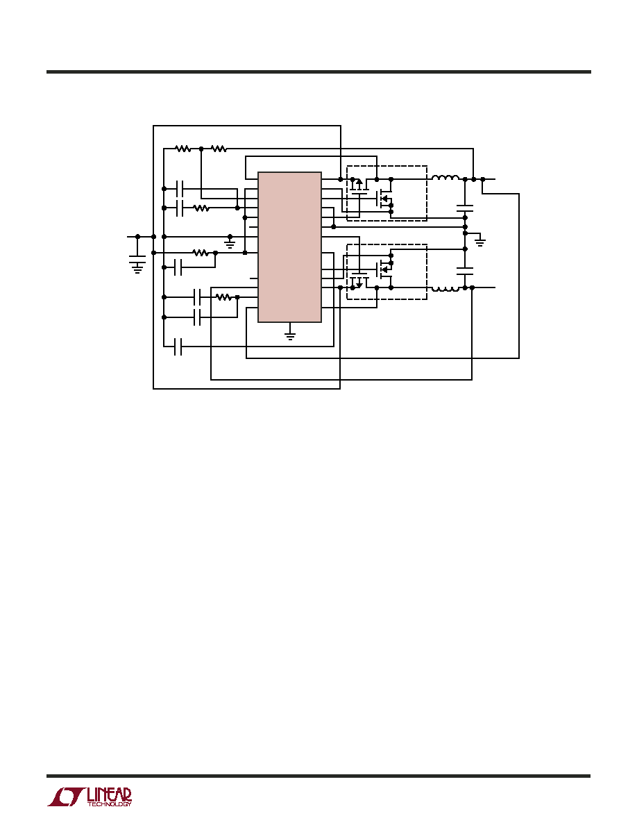
23
LTC3776
3776f
TYPICAL APPLICATIO S
U
Figure 14. 2-Phase, 550kHz, DDR Memory Supplies
SGND
PLLLPF
IPRG2
IPRG1
V
FB1
I
TH1
SW1
R
VIN
10
R
ITH2
6.2k
C
ITH2
2.2nF
C
SS
10nF
C
IN
10µF
◊2
C
VIN
1µF
V
IN
5V
V
IN
C
ITH2B
330pF
R
ITH1
22k
C
ITH1
1000pF
C
ITH1A
100pF
R
FB1B
187k
R
FB1A
59k
PGOOD
V
FB2
V
REF
25
I
TH2
TG2
LTC3776EUF
PGND
TG1
SYNC/SSEN
BG1
PGND
22
21
20
19
18
17
16
15
14
13
12
11
10
23
24
1
2
3
4
5
9
8
7
6
SENSE1
+
MP1
MP2
L1
1.5µH
L2
1.5µH
MN1
Si7540DP
MN2
Si7540DP
RUN/SS
BG2
PGND
PGND
SW2
SENSE2
+
C
OUT2
100µF
C
OUT1
100µF
V
DDQ
2.5V
5A
V
TT
1.25V
±5A
3776 F14

24
LTC3776
3776f
TYPICAL APPLICATIO S
U
Figure 15. 2-Phase, 750kHz, DDR Memory Supplies with Ceramic Output Capacitors
SGND
PLLLPF
IPRG2
IPRG1
V
FB1
I
TH1
SW1
R
VIN
10
R
ITH2
6.2k
C
ITH2
2.2nF
C
SS
10nF
C
IN
22µF
C
VIN
1µF
V
IN
3.3V
V
IN
C
ITH2A
330pF
R
ITH1
22k
C
ITH1
1000pF
C
ITH1A
100pF
R
FB1B
187k
R
FB1A
59k
PGOOD
V
FB2
V
REF
PGND
I
TH2
TG2
LTC3776EUF
PGND
TG1
SYNC/SSEN
BG1
PGND
22
21
20
19
18
17
16
15
14
13
12
11
10
25
23
24
1
2
3
4
5
9
8
7
6
SENSE1
+
MP1
FDC638P
MP2
FDC638P
L1
2.2µH
L2
2.2µH
MN1
FDC637N
MN2
FDC637N
RUN/SS
BG2
PGND
SW2
SENSE2
+
C
OUT2
47µF
C
OUT1
47µF
V
DDQ
2.5V
2A
V
TT
1.25V
±2A
3776 F15
L1, L2: VISHAY IHLP-2525CZ-01

25
LTC3776
3776f
TYPICAL APPLICATIO S
U
Figure 16. 2-Phase, Synchronizable, DDR Memory Supplies
SGND
PLLLPF
IPRG2
IPRG1
V
FB1
I
TH1
SW1
R
VIN
10
R
ITH2
15k
C
ITH2
220pF
C
IN
22µF
C
VIN
1µF
V
IN
3.3V
V
IN
R
ITH1
15k
C
ITH1
220pF
C
FF1
100pF
C
LP
10nF
R
LP
15k
R
FB1B
187k
R
FB1A
59k
PGOOD
V
FB2
V
REF
I
TH2
TG2
LTC3776EGN
PGND
TG1
SYNC/SSEN
BG1
PGND
1
24
23
22
21
20
19
18
17
16
15
14
13
C
OUT1
, C
OUT2
: SANYO 4TPB150MC
D1, D2: OPTIONAL SCHOTTKY DIODES
L1, L2: VISHAY IHLP-2525CZ-01
2
3
4
5
6
7
5
12
11
10
9
SENSE1
+
MP1
SW1
SW2
CLK IN
MP2
L1
1.5µH
L2
1.5µH
MN1
Si7540DP
MN2
Si7540DP
RUN/SS
BG2
PGND
SW2
SENSE2
+
C
OUT2
150µF
C
OUT1
150µF
V
DDQ
2.5V
4A
V
TT
1.25V
±4A
3736 F16
+
+
D1
D2
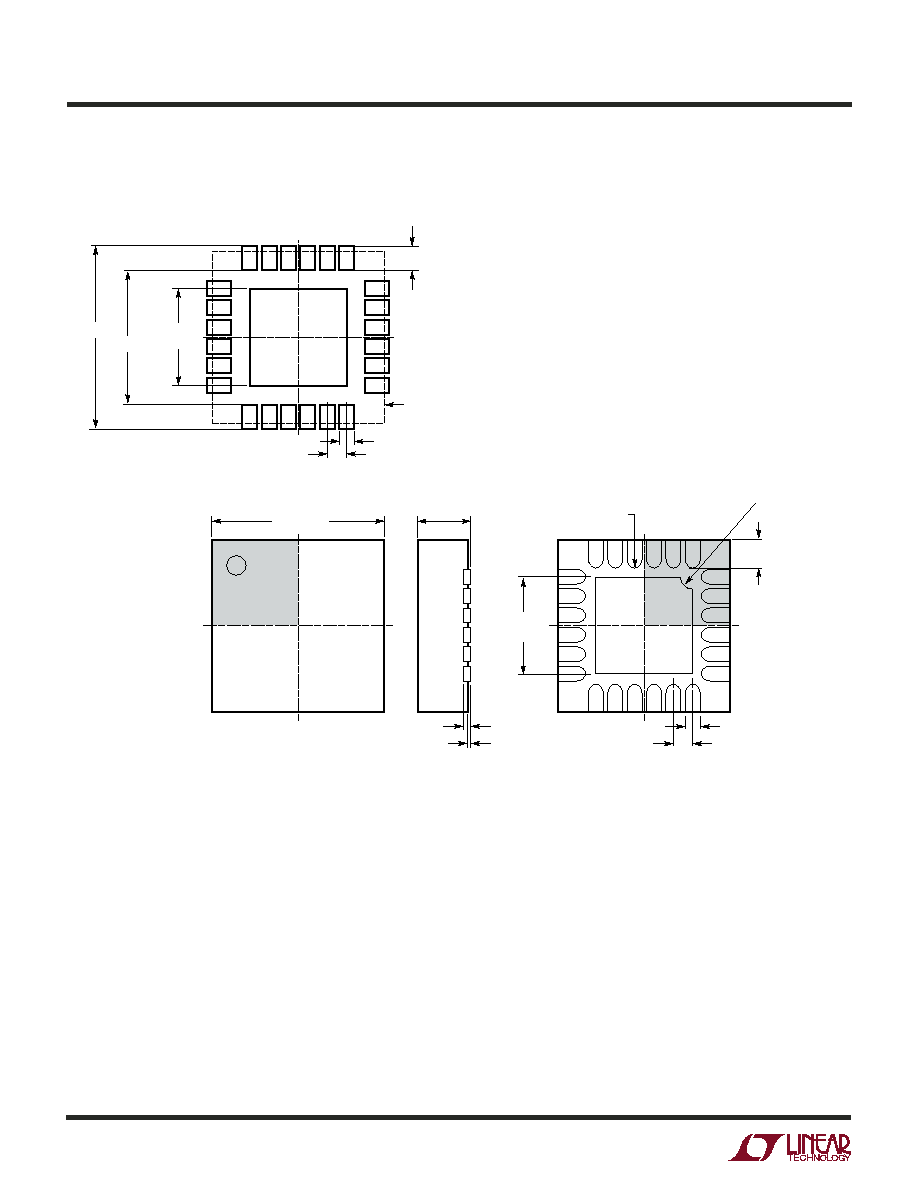
26
LTC3776
3776f
U
PACKAGE DESCRIPTIO
UF Package
24-Lead Plastic QFN (4mm ◊ 4mm)
(Reference LTC DWG # 05-08-1697)
4.00 ± 0.10
(4 SIDES)
NOTE:
1. DRAWING PROPOSED TO BE MADE A JEDEC PACKAGE OUTLINE MO-220 VARIATION (WGGD-X)--TO BE APPROVED
2. DRAWING NOT TO SCALE
3. ALL DIMENSIONS ARE IN MILLIMETERS
4. DIMENSIONS OF EXPOSED PAD ON BOTTOM OF PACKAGE DO NOT INCLUDE
MOLD FLASH. MOLD FLASH, IF PRESENT, SHALL NOT EXCEED 0.15mm ON ANY SIDE, IF PRESENT
5. EXPOSED PAD SHALL BE SOLDER PLATED
6. SHADED AREA IS ONLY A REFERENCE FOR PIN 1 LOCATION
ON THE TOP AND BOTTOM OF PACKAGE
PIN 1
TOP MARK
(NOTE 6)
0.40 ± 0.10
24
23
1
2
BOTTOM VIEW--EXPOSED PAD
2.45 ± 0.10
(4-SIDES)
0.75 ± 0.05
R = 0.115
TYP
0.25 ± 0.05
0.50 BSC
0.200 REF
0.00 ≠ 0.05
(UF24) QFN 0105
RECOMMENDED SOLDER PAD PITCH AND DIMENSIONS
0.70 ±0.05
0.25 ±0.05
0.50 BSC
2.45 ± 0.05
(4 SIDES)
3.10 ± 0.05
4.50 ± 0.05
PACKAGE OUTLINE
PIN 1 NOTCH
R = 0.20 TYP OR
0.35 ◊ 45∞ CHAMFER

27
LTC3776
3776f
U
PACKAGE DESCRIPTIO
GN Package
24-Lead Plastic SSOP (Narrow .150 Inch)
(Reference LTC DWG # 05-08-1641)
.337 ≠ .344*
(8.560 ≠ 8.738)
GN24 (SSOP) 0204
1
2
3
4
5
6
7
8
9 10 11 12
.229 ≠ .244
(5.817 ≠ 6.198)
.150 ≠ .157**
(3.810 ≠ 3.988)
16
17
18
19
20
21
22
23
24
15 1413
.016 ≠ .050
(0.406 ≠ 1.270)
.015 ± .004
(0.38 ± 0.10)
◊ 45∞
0∞ ≠ 8∞ TYP
.0075 ≠ .0098
(0.19 ≠ 0.25)
.0532 ≠ .0688
(1.35 ≠ 1.75)
.008 ≠ .012
(0.203 ≠ 0.305)
TYP
.004 ≠ .0098
(0.102 ≠ 0.249)
.0250
(0.635)
BSC
.033
(0.838)
REF
.254 MIN
RECOMMENDED SOLDER PAD LAYOUT
.150 ≠ .165
.0250 BSC
.0165 ± .0015
.045 ±.005
*DIMENSION DOES NOT INCLUDE MOLD FLASH. MOLD FLASH
SHALL NOT EXCEED 0.006" (0.152mm) PER SIDE
**DIMENSION DOES NOT INCLUDE INTERLEAD FLASH. INTERLEAD
FLASH SHALL NOT EXCEED 0.010" (0.254mm) PER SIDE
INCHES
(MILLIMETERS)
NOTE:
1. CONTROLLING DIMENSION: INCHES
2. DIMENSIONS ARE IN
3. DRAWING NOT TO SCALE
Information furnished by Linear Technology Corporation is believed to be accurate and reliable.
However, no responsibility is assumed for its use. Linear Technology Corporation makes no represen-
tation that the interconnection of its circuits as described herein will not infringe on existing patent rights.

28
LTC3776
3776f
PART NUMBER
DESCRIPTION
COMMENTS
LTC1735
High Efficiency Synchronous Step-Down Controller
Burst Mode Operation, 16-Pin Narrow SSOP, Fault Protection,
3.5V V
IN
36V
LTC1772
Constant Frequency Current Mode Step-Down
2.5V V
IN
9.8V, I
OUT
Up to 4A, SOT-23 Package, 550kHz
DC/DC Controller
LTC1778
No R
SENSE
TM
Synchronous Step-Down Controller
Current Mode Operation Without Sense Resistor,
Fast Transient Response, 4V V
IN
36V
LTC2923
Power Supply Tracking Controller
Controls Up to Three Supplies, 10-Lead MSOP
LTC3411
1.25A (I
OUT
), 4MHz, Synchronous Step-Down DC/DC Converter
95% Efficiency, V
IN
: 2.5V to 5.5V, V
OUT
= 0.8V, I
Q
= 60µA,
I
SD
= <1µA, MS Package
LTC3412
2.5A (I
OUT
), 4MHz, Synchronous Step-Down DC/DC Converter
95% Efficiency, V
IN
: 2.5V to 5.5V, V
OUT
= 0.8V, I
Q
= 60µA,
I
SD
= <1µA, TSSOP-16E Package
LTC3413
3A Monolithic DDR Memory Termination Regulator
±3A Output Current, 2.25V V
IN
5.5V
LTC3701
2-Phase, Low Input Voltage Dual Step-Down DC/DC Controller
2.5V V
IN
9.8V, 550kHz, PGOOD, PLL, 16-Lead SSOP
LTC3708
Fast 2-Phase, No R
SENSE
Buck Controller with
Constant On-Time Dual Controller, V
IN
Up to 36V, Very Low
Output Tracking
Duty Cycle Operation, 5mm ◊ 5mm QFN Package
LTC3717
High Power DDR Memory Termination Regulator
4V V
IN
36V, V
OUT
Tracks V
IN
or V
REF
, I
OUT
from 1A to 20A
LTC3728/LTC3728L
Dual, 550kHz, 2-Phase Synchronous Step-Down
Constant Frequency, V
IN
to 36V, 5V and 3.3V LDOs,
Switching Regulator
5mm ◊ 5mm QFN or 28-Lead SSOP
LTC3736
Dual, 2-Phase, No R
SENSE
, Synchronous Controller
V
IN
: 2.75 to 9.8V, I
OUT
up to 5A, 4mm x 4mm QFN Package
with Output Tracking
LTC3736-1
Dual, 2-Phase, No R
SENSE
, Synchronous Controller
V
IN
: 2.75 to 9.8V, Spread Spectrum Operation, Output Voltage
with Spread Spectrum
Tracking, 4mm x 4mm QFN Package
LTC3737
Dual, 2-Phase, No R
SENSE
, Controller
V
IN
: 2.75 to 9.8V, I
OUT
up to 5A, 4mm x 4mm QFN Package
with Output Tracking
LTC3831
High Power DDR Memory Termination Regulator
V
OUT
Tracks 1/2 V
IN
or V
REF
, 3V V
IN
8V, I
OUT
from 1A to 20A
No R
SENSE
is a trademark of Linear Technology Corporation.
LT/TP 0205 1K ∑ PRINTED IN USA
© LINEAR TECHNOLOGY CORPORATION 2005
RELATED PARTS
Linear Technology Corporation
1630 McCarthy Blvd., Milpitas, CA 95035-7417
(408) 432-1900
FAX: (408) 434-0507
www.linear.com
TYPICAL APPLICATIO
U
2-Phase, Spread Spectrum, DDR Memory Supplies with Ceramic Output Capacitors
SGND
PLLLPF
IPRG2
IPRG1
V
FB1
I
TH1
SW1
R
VIN
10
2200pF
R
ITH2
6.2k
C
ITH2
2.2nF
C
SS
10nF
C
IN
22µF
C
VIN
1µF
V
IN
3.3V
V
IN
C
ITH2A
330pF
R
ITH1
22k
C
ITH1
1000pF
C
ITH1A
100pF
R
FB1B
187k
R
FB1A
59k
PGOOD
V
FB2
V
REF
PGND
I
TH2
TG2
LTC3776EUF
PGND
TG1
SYNC/SSEN
BG1
PGND
22
21
20
19
18
17
16
15
14
13
12
11
10
25
23
24
1
2
3
4
5
9
8
7
6
SENSE1
+
MP1
FDC638P
MP2
FDC638P
L1
2.2µH
L2
2.2µH
MN1
FDC637N
MN2
FDC637N
RUN/SS
BG2
PGND
SW2
SENSE2
+
C
OUT2
47µF
C
OUT1
47µF
V
DDQ
2.5V
2A
V
TT
1.25V
±2A
3776 TA02
L1, L2: VISHAY IHLP-2525CZ-01