 | –≠–ª–µ–∫—Ç—Ä–æ–Ω–Ω—ã–π –∫–æ–º–ø–æ–Ω–µ–Ω—Ç: LTC3783 | –°–∫–∞—á–∞—Ç—å:  PDF PDF  ZIP ZIP |

1
LTC3783
3783f
High Voltage LED Arrays
Telecom Power Supplies
42V Automotive Systems
24V Industrial Controls
IP Phone Power Supplies
PWM LED Driver and Boost,
Flyback and SEPIC Controller
True Color PWM
TM
Delivers Constant Color with
3000:1 Dimming Ratio
Fully Integrated Load FET Driver for PWM Dimming
Control of High Power LEDs
100:1 Dimming from Analog Inputs
Wide FB Voltage Range: 0V to 1.23V
Constant Current or Constant Voltage Regulation
Low Shutdown Current: I
Q
= 20
µA
1% 1.23V Internal Voltage Reference
2% RUN Pin Threshold with 100mV Hysteresis
Programmable Operating Frequency (20kHz to
1MHz) with One External Resistor
Synchronizable to an External Clock Up to 1.3f
OSC
Internal 7V Low Dropout Voltage Regulator
Programmable Output Overvoltage Protection
Programmable Soft-Start
Can be Used in a No R
SENSE
TM
Mode for V
DS
< 36V
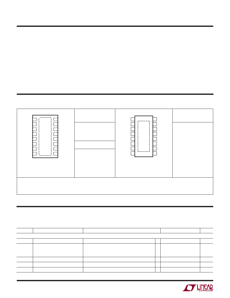
16-Lead DFN and TSSOP Packages
FEATURES
DESCRIPTIO
U
APPLICATIO S
U
TYPICAL APPLICATIO
U
The LTC
Æ
3783 is a current mode LED driver and boost,
flyback and SEPIC controller that drives both an N-channel
power MOSFET and an N-channel load PWM switch.
When using an external load switch, the PWMIN input not
only drives PWMOUT, but also enables controller GATE
switching and error amplifier operation, allowing the con-
troller to store load current information while PWMIN is
low. This feature (patent pending) provides extremely fast,
true PWM load switching with no transient overvoltage or
undervoltage issues; LED dimming ratios of 3000:1 can be
achieved digitally, avoiding the color shift normally asso-
ciated with LED current dimming. The FBP pin allows
analog dimming of load current, further increasing the
effective dimming ratio by 100:1 over PWM alone.
In applications where output load current must be re-
turned to V
IN
, optional constant current/constant voltage
regulation controls either output (or input) current or
output voltage and provides a limit for the other. I
LIM
provides a 10:1 analog dimming ratio.
For low- to medium-power applications, No R
SENSE
mode
can utilize the power MOSFET's on-resistance to eliminate
the current-sense resistor, thereby maximizing efficiency.
The IC's operating frequency can be set with an external
resistor over a 20kHz to 1MHz range and can be synchro-
nized to an external clock using the SYNC pin.
The LTC3783 is available in the 16-lead DFN and TSSOP
packages.
, LTC and LT are registered trademarks of Linear Technology Corporation.
True Color PWM and No R
SENSE
are trademarks of Linear Technology Corporation.
All other trademarks are the property of their respective owners. Patent pending.
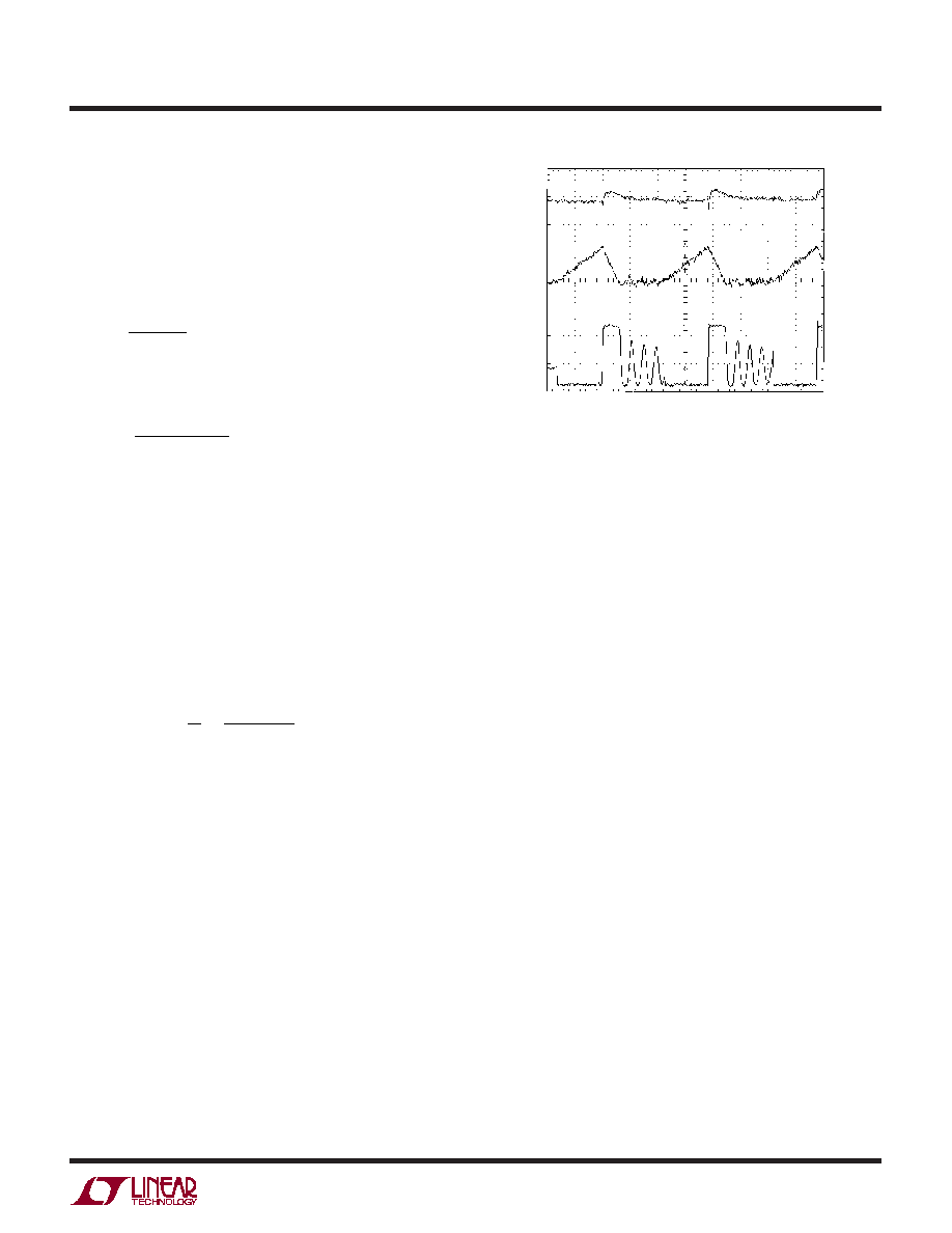
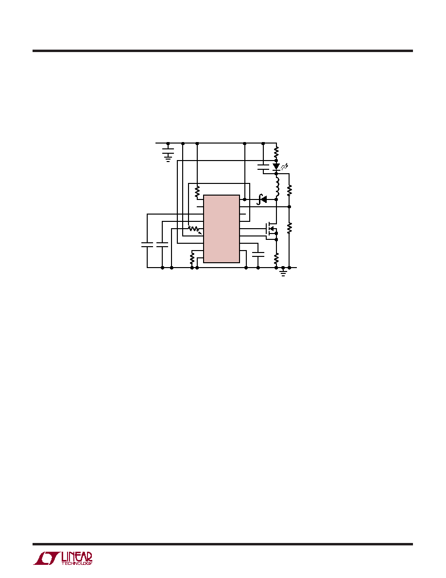
350mA PWM LED Boost Application
LTC3783
1M
RUN
PWMIN
I
TH
SS
V
REF
FBP
FBN
FREQ
SYNC
V
IN
OV/FB
PWMOUT
I
LIM
GATE
SENSE
INTV
CC
GND
LED*
STRING
V
IN
6V TO 16V
(< TOTAL V
F
OF LEDs)
GND
M1
M1, M2: SILICONIX Si4470EY
10
µF
◊2
ZETEX ZLL51000
M2
C
OUT
10
µF
V
OUT
<25V
*LUMILEDS LHXL-BW02
3783 TA01a
0.1
µF
10k
6k
105k
10
µF
2.2
µH
4.7
µF
0.05
237k
12.4k
0.3
Typical Waveforms
V
PWMIN
5V/DIV
I
L
2.5A/DIV
I
LED
0.5A/DIV
V
OUT
0.2V/DIV
AC COUPLED
1
µs/DIV
3783 TA01b
2
LTC3783
3783f
V
IN
, SENSE, FBP, FBN Voltages ................ ≠ 0.3V to 42V
INTV
CC
Voltage ........................................... ≠ 0.3V to 9V
INTV
CC
Output Current ........................................ 75mA
GATE Output Current ................................ 50mA (RMS)
PWMOUT Output Current ......................... 25mA (RMS)
V
REF
Ouput Current ................................................ 1mA
GATE, PWMOUT Voltages ..... ≠0.3V to (V
INTVCC
+ 0.3V)
I
TH
, I
LIM
, SS Voltages .............................. ≠ 0.3V to 2.7V
RUN, SYNC, PWMIN Voltages .................... ≠ 0.3V to 7V
Consult LTC Marketing for parts specified with wider operating temperature ranges.
ABSOLUTE AXI U RATI GS
W
W
W
U
PACKAGE/ORDER I FOR ATIO
U
U
W
(Note 1)
LTC3783EDHD
ORDER PART
NUMBER
DHD PART MARKING
3783
T
JMAX
= 125
∞C,
JA
= 43
∞C/ W
EXPOSED PAD (PIN 17) IS GND
MUST BE SOLDERED TO PCB
FREQ, V
REF
, OV/FB Voltages .....................≠ 0.3V to 1.5V
Operating Junction Temperature Range
(Note 2) .................................................. ≠ 40
∞C to 85∞C
Junction Temperature (Note 3) ............ ≠ 40
∞C to 125∞C
Storage Temperature Range
DFN Package ................................... ≠ 65
∞C to 125∞C
TSSOP Package ............................... ≠ 65
∞C to 150∞C
Lead Temperature (Soldering, 10sec)
TSSOP Package ............................................... 300
∞C
LTC3783EFE
ORDER PART
NUMBER
16
15
14
13
12
11
10
9
17
1
2
3
4
5
6
7
8
RUN
I
TH
OV/FB
SS
SENSE
V
IN
INTV
CC
GATE
FBN
FBP
I
LIM
V
REF
FREQ
SYNC
PWMIN
PWMOUT
TOP VIEW
DHD PACKAGE
16-LEAD (5mm
◊ 4mm) PLASTIC DFN
FE PACKAGE
16-LEAD PLASTIC TSSOP
1
2
3
4
5
6
7
8
TOP VIEW
16
15
14
13
12
11
10
9
FBN
FBP
I
LIM
V
REF
FREQ
SYNC
PWMIN
PWMOUT
RUN
I
TH
OV/FB
SS
SENSE
V
IN
INTV
CC
GATE
17
T
JMAX
= 125
∞C,
JA
= 38
∞C/ W
EXPOSED PAD (PIN 17) IS GND
MUST BE SOLDERED TO PCB
The
denotes specifications which apply over the full operating temperature range, otherwise specifications are T
A
= 25
∞C.
V
IN
= 12V, V
RUN
= 1.5V, V
SYNC
= 0V, V
FBP
= V
REF
, R
T
= 20k, unless otherwise specified.
ELECTRICAL CHARACTERISTICS
SYMBOL
PARAMETER
CONDITIONS
MIN
TYP
MAX
UNITS
Main Control Loop/Whole System
V
IN
Input Voltage Range
3
36
V
I
Q
Input Voltage Supply Current
(Note 4)
Continuous Mode
V
OV/FB
= 1.5V, V
ITH
= 0.75V
1.5
mA
Shutdown Mode
V
RUN
= 0V
20
µA
V
RUN
+
Rising RUN Input Threshold Voltage
1.348
V
V
RUN
≠
Falling RUN Input Threshold Voltage
1.223
1.248
1.273
V
V
RUN(HYST)
RUN Pin Input Threshold Hysteresis
100
mV
Order Options Tape and Reel: Add #TR
Lead Free: Add #PBF Lead Free Tape and Reel: Add #TRPBF
Lead Free Part Marking:
http://www.linear.com/leadfree/
3
LTC3783
3783f
The
denotes specifications which apply over the full operating temperature range, otherwise specifications are T
A
= 25
∞C.
V
IN
= 12V, V
RUN
= 1.5V, V
SYNC
= 0V, V
FBP
= V
REF
, R
T
= 20k, unless otherwise specified.
ELECTRICAL CHARACTERISTICS
SYMBOL
PARAMETER
CONDITIONS
MIN
TYP
MAX
UNITS
I
RUN
RUN Pin Input Current
5
nA
V
SENSE(MAX)
Maximum Current Sense Threshold
125
150
180
mV
I
SENSE(ON)
SENSE Pin Current (GATE High)
V
SENSE
= 0V
70
µA
I
SENSE(OFF)
SENSE Pin Current (GATE Low)
V
SENSE
= 36V
0.2
µA
I
SS
Soft-Start Pin Output Current
V
SS
= 0V
≠50
µA
Voltage/Temperature Reference
V
REF
Reference Voltage
1.218
1.230
1.242
V
1.212
1.248
V
I
REF
Max Reference Pin Output Current
0.5
mA
V
REF
/
V
IN
Reference Voltage Line Regulation
3V
V
IN
36V
0.002
0.02
%/V
V
REF
/
I
REF
Reference Voltage Load Regulation
0mA
I
REF
0.5mA
0.2
1.0
%/mA
T
MAX
Overtemperature SD Threshold
165
∞C
Rising
T
HYST
Overtemperature Hysteresis
25
∞C
Error Amplifier
I
OV/FB
OV/FB Pin Input Current
18
60
nA
V
OV/FB(OV)
OV/FB Overvoltage Lockout Threshold V
OV/FB(OV)
≠ V
OV/FB(NOM)
in %, V
FBP
V
REF
7
%
V
OV/FB(FB)
OV/FB Pin Regulation Voltage
2.5V < V
FBP
< 36V
1.212
1.230
1.248
V
I
FBP
, I
FBN
Error Amplifier Input Current
0V
V
FBP
V
REF
≠0.4
µA
2.5V < V
FBP
< 36V
50
µA
V
FBP
≠ V
FBN
Error Amplifier Offset Voltage
0V
V
FBP
V
REF
≠3
3
mV
(Note 5)
2.5V < V
FBP
36V (V
ILIM
= V
REF
)
100
mV
2.5V < V
FBP
36V (V
ILIM
= 0.123V)
10
mV
g
m
Error Amplifier Transconductance
V
FBP
V
REF
1.7
mmho
2.5V < V
FBP
< 36V
14
mmho
A
VOL
Error Amplifier Open-Loop Gain
500
V/V
Oscillator
f
OSC
Oscillator Frequency
R
FREQ
= 20k
250
300
350
kHz
Oscillator Frequency Range
20
1000
kHz
D
MAX
Maximum Duty Cycle
85
90
97
%
f
SYNC
/f
OSC
Recommended Max SYNC Freq Ratio f
OSC
= 300kHz (Note 6)
1.25
1.3
t
SYNC(MIN)
SYNC Minimum Input Pulse Width
V
SYNC
= 0V to 5V
25
ns
t
SYNC(MAX)
SYNC Maximum Input Pulse Width
V
SYNC
= 0V to 5V
0.8/f
OSC
ns
V
IH(SYNC)
SYNC Input Voltage High Level
1.2
V
V
HYST(SYNC)
SYNC Input Voltage Hysteresis
0.5
V
R
SYNC
SYNC Input Pull-Down Resistance
100
k
t
ON(MIN)
Minimum On-time
With Sense Resistor, 10mV Overdrive
170
ns
No R
SENSE
Mode
300
ns
4
LTC3783
3783f
The
denotes specifications which apply over the full operating temperature range, otherwise specifications are T
J
= 25
∞C.
V
IN
= 12V, V
RUN
= 1.5V, V
SYNC
= 0V, V
FBP
= V
REF
, R
T
= 20k, unless otherwise specified.
ELECTRICAL CHARACTERISTICS
SYMBOL
PARAMETER
CONDITIONS
MIN
TYP
MAX
UNITS
Low Dropout Regulator
V
INTVCC
INTV
CC
Regulator Output Voltage
V
OV/FB
= 1.5V
6.5
7
7.5
V
UVLO
INTV
CC
Undervoltage Lockout
Rising INTV
CC
2.3
2.5
V
Thresholds
Falling INTV
CC
1.8
2.1
V
Hysteresis
0.2
V
V
INTVCC
INTV
CC
Line Regulation
12V
V
IN
36V
2
6
mV/V
V
IN
V
LDO(LOAD)
INTV
CC
Load Regulation
0
I
INTVCC
10mA
≠1
≠0.1
%
V
DROPOUT
INTV
CC
Dropout Voltage
V
IN
= 7V, I
INTVCC
= 10mA
300
500
mV
I
INTVCC(SD)
Bootstrap Mode INTV
CC
Supply
V
SENSE
= 0V
25
µA
Current in Shutdown
V
SENSE
= 7V
15
µA
GATE/PWMOUT Drivers
t
r(GATE)
GATE Driver Output Rise Time
C
L
= 3300pF (Note 7)
15
ns
t
f(GATE)
GATE Driver Output Fall Time
C
L
= 3300pF (Note 7)
8
ns
I
PK(GATE,RISE)
GATE Driver Peak Current Sourcing
V
GATE
= 0V
0.5
A
I
PK(GATE,FALL)
GATE Driver Peak Current Sinking
V
GATE
= 7V
1
A
V
PWMIN
PWMIN Pin Input Threshold Voltages
Rising PWMIN
1.6
V
Falling PWMIN
0.8
V
Hysteresis
0.8
V
R
PWMIN
PWMIN Input Pull-Up Resistance
100
k
t
r(PWMOUT)
PWMOUT Driver Output Rise Time
C
L
= 3300pF (Note 7)
30
ns
t
f(PWMOUT)
PWMOUT Driver Output Fall Time
C
L
= 3300pF (Note 7)
16
ns
I
PK(PWMOUT,RISE)
PWMOUT Driver Peak Current Sourcing
V
PWMOUT
= 0V
0.25
A
I
PK(PWMOUT,FALL)
PWMOUT Driver Peak Current Sinking
V
PWMOUT
= 7V
0.50
A
Note 1: Absolute Maximum Ratings are those values beyond which the life
of the device may be impaired.
Note 2: The LTC3783E is guaranteed to meet performance specifications
from 0
∞C to 85∞C junction temperature. Specifications over the ≠40∞C to
85
∞C operating temperature range are assured by design, characterization
and correlation with statistical process controls.
Note 3: T
J
is calculated from the ambient temperature T
A
and power
dissipation P
D
according to the following formula:
T
J
= T
A
+ (P
D
∑ 43
∞C/W) for the DFN
T
J
= T
A
+ (P
D
∑ 38
∞C/W) for the TSSOP
Note 4: The dynamic input supply current is higher due to power MOSFET
gate charging (Q
G
∑ f
OSC
). See Operation section.
Note 5: The LTC3783 is tested in a feedback loop which servos V
FBN
to
V
FBP
= V
VREF
with the I
TH
pin forced to the midpoint of its voltage range
(0.3V
V
ITH
1.2V; midpoint = 0.75V).
Note 6: In a synchronized application, the internal slope compensation is
increased by 25%. Synchronizing to a significantly higher ratio will reduce
the effective amount of slope compensation, which could result in sub-
harmonic oscillation for duty cycles greater than 50%
Note 7: Rise and fall times are measured at 10% and 90% levels.

5
LTC3783
3783f
TYPICAL PERFOR A CE CHARACTERISTICS
U
W
V
REF
vs Temperature
V
REF
Line Regulation
V
REF
Load Regulation
I
Q
vs Temperature (PWMIN Low)
Dynamic I
Q
vs Frequency
RUN Thresholds vs V
IN
RUN Thresholds vs Temperature
R
T
vs Frequency
TEMPERATURE (
∞C)
≠50
V
REF
(V)
1.15
1.20
1.25
3783 G01
1.10
1.05
1.00
0
50
100
150
V
IN
(V)
0
V
REF
(V)
1.229
1.231
40
3783 G02
1.227
1.225
10
20
30
1.235
1.233
I
REF
(mA)
0
V
REF
(V)
1.231
1.233
1.235
4
3783 G03
1.229
1.227
1.225
1
2
3
5
V
IN
= 12V
V
IN
= 2.5V
TEMPERATURE (
∞C)
≠75
I
Q
(mA)
0.6
0.8
1.0
75
175
3783 G04
0.4
0.2
0
≠25
25
125
1.2
1.4
1.6
I
Q
vs V
IN
(PWMIN Low)
V
IN
(V)
0
0
I
Q
(mA)
1.1
1.3
1.4
1.5
20
40
50
2.0
1.9
3783 G05
1.2
10
30
1.6
1.7
1.8
FREQUENCY (MHz)
0
0
DYNAMIC I
Q
(mA)
5
10
15
20
30
0.5
1
3783 G06
1.5
25
C
L
= 3300pF
I
Q(TOT)
= 1.3mA + Q
G
∑ f
V
IN
(V)
0
0.6
RUN THRESHOLDS (V)
0.7
0.9
1.0
1.1
1.6
1.3
10
20
3783 G07
0.8
1.4
1.5
1.2
30
40
RUN HIGH
RUN LOW
TEMPERATURE (
∞C)
≠50
RUN THRESHOLDS (V)
1.32
1.34
1.36
150
3783 G08
1.30
1.28
1.22
0
50
100
1.26
1.24
1.40
1.38
RUN HIGH
RUN LOW
FREQUENCY (kHz)
10
R
T
(k
)
100
1
100
1000
10000
3783 G09
1
10
1000
T
A
= 25
∞C unless otherwise specified

6
LTC3783
3783f
Frequency vs Temperature
Maximum V
SENSE
vs Temperature
INTV
CC
Load Regulation
INTV
CC
Line Regulation
INTV
CC
Load Regulation
Over Temperature
INTV
CC
Line Regulation
vs Temperature
I
SS
Soft-Start Current
vs Temperature
Gate Rise/Fall Time
vs Capacitance
TEMPERATURE (
∞C)
≠50
250
FREQUENCY (kHz)
260
280
290
300
350
320
0
50
3783 G10
270
330
340
310
100
150
I
SENSE
vs Temperature
TEMPERATURE (
∞C)
≠50
V
SENSE
(V)
152
156
160
3783 G11
148
144
150
154
158
146
142
140
0
50
100
150
TEMPERATURE (
∞C)
≠50
65
I
SENSE
(
µ
A)
66
68
69
70
75
72
0
50
3783 G12
67
73
74
71
100
150
I
INTVCC
(mA)
0
6.50
6.55
6.80
6.75
6.70
INTV
CC
(V)
6.85
6.90
6.95
7.00
0.02 0.04 0.06 0.08
3783 G13
0.10 0.12 0.14 0.16
V
IN
(V)
0
INTV
CC
(V)
6.80
6.90
7.00
7.05
40
3783 G14
6.70
6.60
6.75
6.85
6.95
6.65
6.55
10
20
30
50
I
INTVCC
(mA)
0
5.0
INTV
CC
(V)
5.4
5.6
5.8
6.0
6.2
6.4
50
100
3783 G15
6.6
6.8
7.0
5.2
150
≠50
∞C, ≠25∞C, 0∞C
50
∞C
100
∞C
125
∞C
25
∞C
75
∞C
150
∞C
V
IN
(V)
5
6.90
INTV
CC
(V)
6.95
7.00
7.05
7.10
7.15
7.20
15
10
20
25
35
30
40
3783 G16
150
∞C
25
∞C
≠50
∞C
TEMPERATURE (
∞C)
≠50
47.8
SOFT-START CURRENT (
µ
A)
48.0
48.4
48.6
48.8
50.0
49.8
49.2
0
50
3783 G17
48.2
49.4
49.6
49.0
100
150
CAPACITANCE (nF)
0
TIME (ns)
40
50
60
20
3783 G18
30
20
0
5
10
15
10
80
70
GATE TR
GATE TF
TYPICAL PERFOR A CE CHARACTERISTICS
U
W
T
A
= 25
∞C unless otherwise specified

7
LTC3783
3783f
U
U
U
PI FU CTIO S
FBN (Pin 1): Error Amplifier Inverting Input/Negative
Current Sense Pin. In voltage mode (V
FBP
V
VREF
), this
pin senses feedback voltage from either the external
resistor divider across V
OUT
for output voltage regula-
tion, or the grounded sense resistor under the load for
output current regulation. In constant current/constant
voltage mode (V
FBP
> 2.5V), connect this pin to the
negative side of the current-regulating resistor. Nominal
voltage for this pin in regulation is either V
FBP
or (V
FBP
≠
100mV) for V
ILIM
= 1.23V, depending on operational
mode (voltage or constant current/constant voltage) set
by the voltage at V
FBP
.
FBP (Pin 2): Error Amplifier Noninverting Input/Positive
Current Sense Pin. This pin voltage determines the control
loop's feedback mode (voltage or constant current/con-
stant voltage), the threshold of which is approximately 2V.
In voltage mode (V
FBP
V
REF
), this pin represents the
desired voltage which the regulated loop will cause FBN to
follow. In constant current/constant voltage mode (V
FBP
>
2.5V), connect this pin to the positive side of the load
current-sensing resistor. The acceptable input ranges for
this pin are 0V to 1.23V (voltage mode) and 2.5V to 36V
(constant current/constant voltage mode).
I
LIM
(Pin 3): Current Limit Pin. Sets current sense resistor
offset voltage (V
FBP
≠ V
FBN
) in constant current mode
regulation (i.e., when V
FBP
> 2.5V). Offset voltage is
100mV when V
ILIM
= 1.23V and decreases proportionally
with V
ILIM
. Nominal voltage range for this pin is 0.1V to
1.23V.
V
REF
(Pin 4): Reference Voltage Pin. Provides a buffered
version of the internal bandgap voltage, which can be
connected to FBP either directly or with attenuation.
Nominal voltage for this pin is 1.23V. This pin should never
be bypassed by a capacitor to GND. Instead, a 10k resistor
to GND should be used to lower pin impedance in noisy
systems.
FREQ (Pin 5): A resistor from the FREQ pin to ground
programs the operating frequency of the chip. The nomi-
nal voltage at the FREQ pin is 0.615V.
SYNC (Pin 6): This input allows for synchronizing the
operating frequency to an external clock and has an
internal 100k pull-down resistor.
PWMIN (Pin 7): PWM Gate Driver Input. Internal 100k
pull-up resistor. While PWMIN is low, PWMOUT is low,
GATE stops switching and the external I
TH
network is
disconnected, saving the I
TH
state.
PWMOUT (Pin 8): PWM Gate Driver Output. Used for
constant current dimming (LED load) or for output discon-
nect (step-up power supply).
GATE (Pin 9): Main Gate Driver Output for the Boost
Converter.
INTV
CC
(Pin 10): Internal 7V Regulator Output. The main
and PWM gate drivers and control circuits are powered
from this voltage. Decouple this pin locally to the IC
ground with a minimum of 4.7
µF low ESR ceramic
capacitor.
V
IN
(Pin 11): Main Supply Pin. Must be closely decoupled
to ground.
SENSE (Pin 12): Current Sense Input for the Control
Loop. Connect this pin to the drain of the main power
MOSFET for V
DS
sensing and highest efficiency for V
SENSE
36V. Alternatively, the SENSE pin may be connected to
a resistor in the source of the main power MOSFET.
Internal leading-edge blanking is provided for both sens-
ing methods.
SS (Pin 13): Soft-Start Pin. Provides a 50
µA pull-up
current, enabled and reset by RUN, which charges an
optional external capacitor. This voltage ramp translates
into a corresponding current limit ramp through the main
MOSFET.
OV/FB (Pin 14): Overvoltage Pin/Voltage Feedback Pin. In
voltage mode (V
FBP
V
REF
), this input, connected to V
OUT
through a resistor network, sets the output voltage at
which GATE switching is disabled in order to prevent an
overvoltage situation. Nominal threshold voltage for the
OV pin is 1.32V (V
REF
+ 7%) with 20mV hysteresis. In
current/voltage mode (V
FBP
> 2.5V), this pin senses V
OUT
through a resistor divider and brings the loop into voltage
regulation such that pin voltage approaches V
REF
= 1.23V,
provided the loop is not regulating the load current (e.g.,
[V
FBP
≠ V
FBN
] < 100mV for I
LIM
= 1.23V).

8
LTC3783
3783f
U
U
U
PI FU CTIO S
I
TH
(Pin 15): Error Amplifier Output/Compensation Pin. The
current comparator input threshold increases with this
control voltage, which is the output of the g
m
type error
amplifier. Nominal voltage range for this pin is 0V to 1.40V.
RUN (Pin 16): The RUN pin provides the user with an
accurate means for sensing the input voltage and pro-
gramming the start-up threshold for the converter. The
falling RUN pin threshold is nominally 1.248V and the
comparator has 100mV hysteresis for noise immunity.
When the RUN pin is grounded, the IC is shut down and the
V
IN
supply current is kept to a low value (20
µA typ).
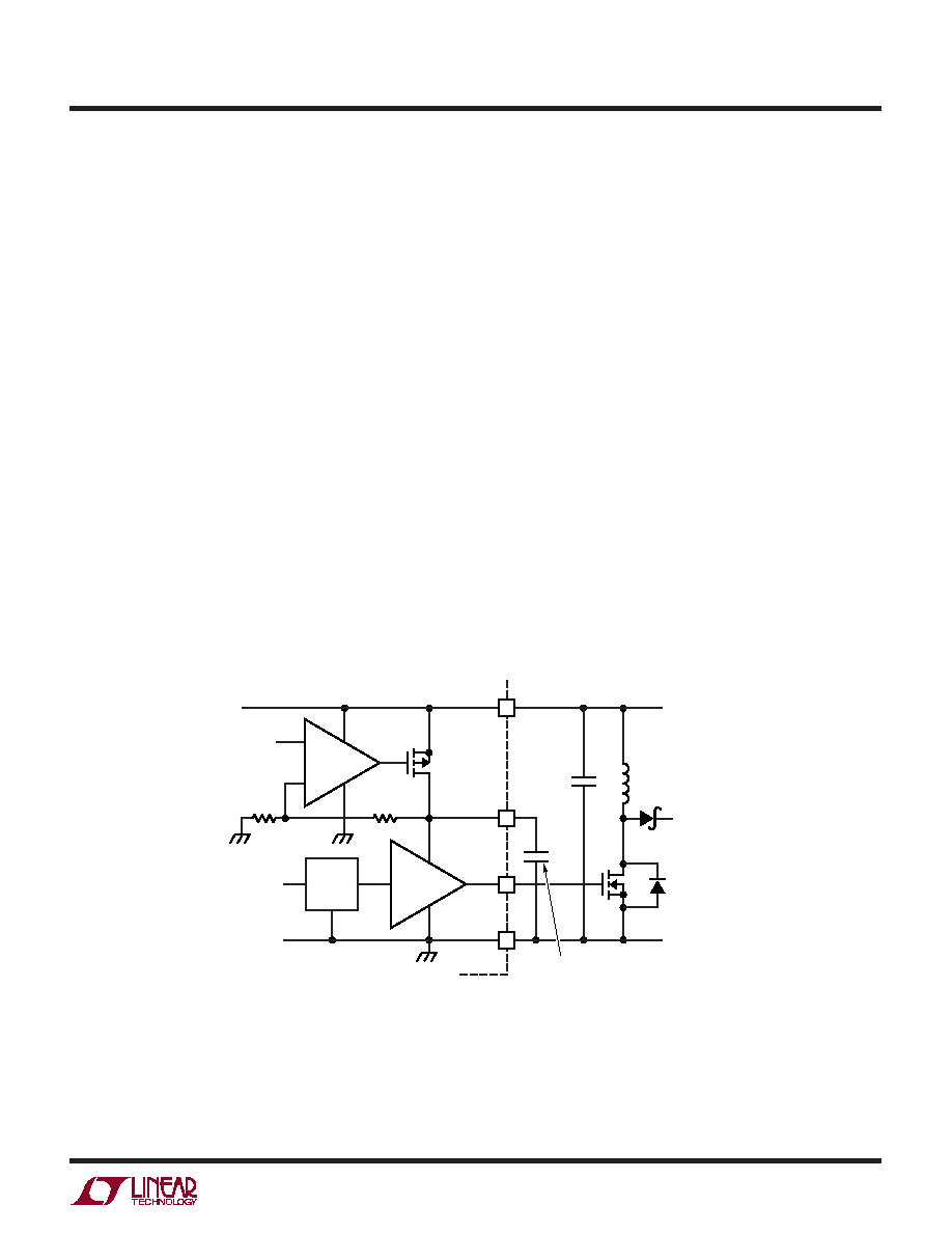
Exposed Pad (Pin 17): Ground Pin. Solder to PCB ground
for electrical contact and rated thermal performance.
BLOCK DIAGRA
W
OSC
V-TO-I
V-TO-I
LDO
BIAS AND
START-UP
9
+
≠
≠
+
≠
LOGIC
V
REF
BIAS
SLOPE
COMP
TEMP
SENSOR
(165
∞C)
OT
SS_RESET
Q
0.615V
FREQ
GATE
12
SENSE
8
PWMOUT
11
V
IN
16
RUN
3738 BD
UV
ITRIP
17
GND
4
V
REF
S
R
OV
CLK
SLEEP
EN
OV/FB
V
REF
1 S
0
5
SYNC
6
I
LIM
3
FBP
FBN
2
1
OV/FB
14
SS
13
+
≠
50
µA
0.2V
+
≠
+
≠
IMAX
0.15V
+
≠
V
REF
+
≠
1.9V
IVMODE
V
REF
+
≠
I
TH
15
PWMIN
7
2.23V
V
REF
+
≠
INTV
CC
10
A
EA

9
LTC3783
3783f
OPERATIO
U
Main Control Loop
The LTC3783 is a constant frequency, current mode
controller for PWM LED as well as DC/DC boost, SEPIC
and flyback converter applications. In constant current
LED applications, the LTC3783 provides an especially
wide PWM dimming range due to its unique switching
scheme, which allows PWM pulse widths as short as
several converter switching periods.
For voltage feedback circuit operation (defined by V
FBP
1.23V), please refer to the Block Diagram of the IC and the
Typical Application on the first page of this data sheet. In
normal operation with PWMIN high, the power MOSFET is
turned on (GATE goes high) when the oscillator sets the
PWM latch, and is turned off when the ITRIP current
comparator resets the latch. Based on the error voltage
represented by (V
FBP
≠ V
FBN
), the error amplifier output
signal at the I
TH
pin sets the ITRIP current comparator
input threshold. When the load current increases, a fall in
the FBN voltage relative to the reference voltage at FBP
causes the I
TH
pin to rise, causing the ITRIP current com-
parator to trip at a higher peak inductor current value. The
average inductor current will therefore rise until it equals
the load current, thereby maintaining output regulation.
When PWMIN goes low, PWMOUT goes low, the I
TH
switch opens and GATE switching is disabled. Lowering
PWMOUT and disabling GATE causes the output capacitor
C
OUT
to hold the output voltage constant in the absence of
load current. Opening the I
TH
switch stores the correct
load current value on the I
TH
capacitor C
ITH
. As a result,
when PWMIN goes high again, both I
TH
and V
OUT
are
instantly at the appropriate levels.
In voltage feedback operation, an overvoltage compara-
tor, OV, senses when the OV/FB pin exceeds the reference
voltage by 7% and provides a reset pulse to the main RS
latch. Because this RS latch is reset-dominant, the power
MOSFET is actively held off for the duration of an output
overvoltage condition.
For constant current/constant voltage regulation opera-
tion (defined by V
FBP
> 2.5V), please refer to the Block
Diagram of the IC and Figure 11. Loop operation is similar
to the voltage feedback, except FBP and FBN now sense
the voltage across sense resistor R
L
in series with the load.
The I
TH
pin now represents the error from the desired
differential set voltage, from 10mV to 100mV, for I
LIM
values of 0.123V to 1.23V. That is, with V
ILIM
= 1.23V, the
loop will regulate such that V
FBP
≠ V
FBN
= 100mV; lower
values of I
LIM
attenuate the difference proportionally.
PWMIN is still functional as above, but will only work
properly if load current can be disconnected by the
PWMOUT signal.
In constant current/constant voltage operation, the OV/FB
pin becomes a voltage feedback pin, which causes the
loop to regulate such that V
OV/FB
= 1.23V, provided the
above current-sense voltage is not reached. In this way,
the loop regulates either voltage or current, whichever
parameter hits its preset limit first.
The nominal operating frequency of the LTC3783 is pro-
grammed using a resistor from the FREQ pin to ground
and can be controlled over a 20kHz to 1MHz range. In
addition, the internal oscillator can be synchronized to an
external clock applied to the SYNC pin and can be locked
to a frequency between 100% and 130% of its nominal
value. When the SYNC pin is left open, it is pulled low by
an internal 100k resistor. With no load, or an extremely
light one, the controller will skip pulses in order to main-
tain regulation and prevent excessive output ripple.
The RUN pin controls whether the IC is enabled or is in a
low current shutdown state. A micropower 1.248V refer-
ence and RUN comparator allow the user to program the
supply voltage at which the IC turns on and off (the RUN
comparator has 100mV of hysteresis for noise immunity).
With the RUN pin below 1.248V, the chip is off and the
input supply current is typically only 20
µA.
10
LTC3783
3783f
The SS pin provides a soft-start current to charge an
external capacitor. Enabled by RUN, the soft-start current
is 50
µA, which creates a positive voltage ramp on V
SS
to
which the internal I
TH
is limited, avoiding high peak
currents on start-up. Once V
SS
reaches 1.23V, the full I
TH
range is established.
The LTC3783 can be used either by sensing the voltage
drop across the power MOSFET or by connecting the
SENSE pin to a conventional shunt resistor in the source
of the power MOSFET, as shown in the Typical Application
on the first page of this data sheet. Sensing the voltage
across the power MOSFET maximizes converter efficiency
and minimizes the component count, but limits the output
voltage to the maximum rating for this pin (36V). By
connecting the SENSE pin to a resistor in the source of the
power MOSFET, the user is able to program output volt-
ages significantly greater than 36V, limited only by other
components' breakdown voltages.
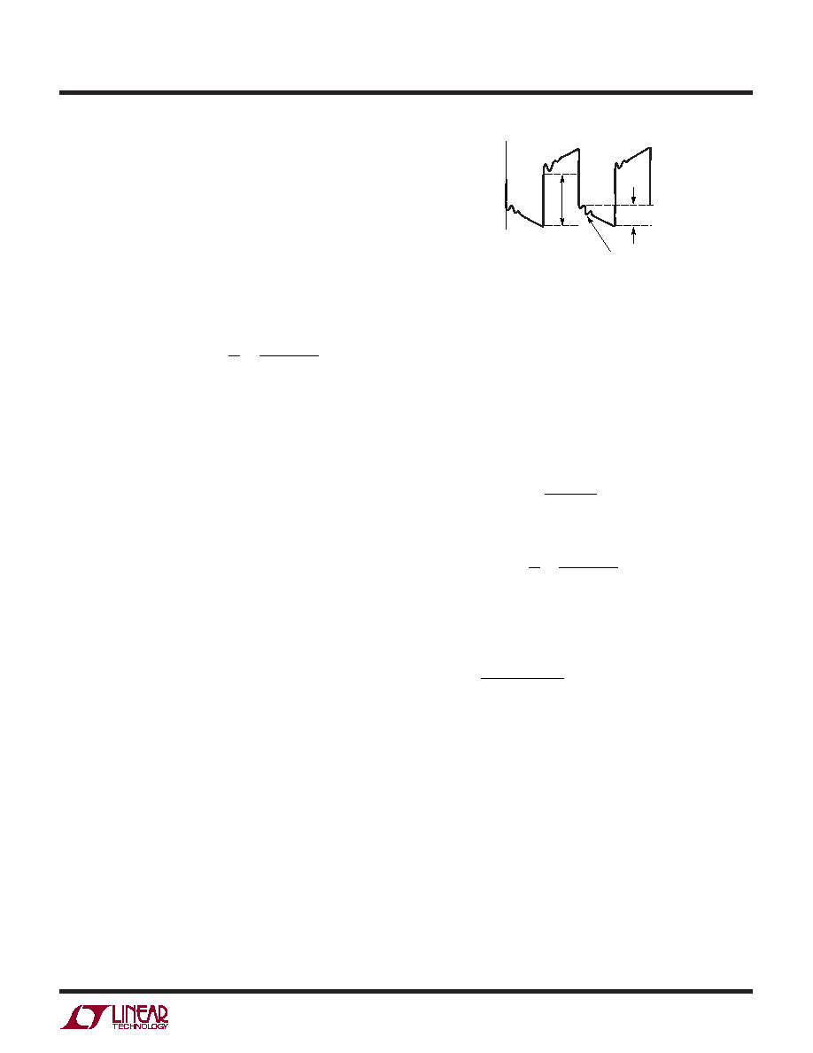
Externally Synchronized Operation
When an external clock signal drives the SYNC pin at a rate
faster than the chip's internal oscillator, the oscillator will
synchronize to it. When the oscillator's internal logic
circuitry detects a synchronizing signal on the SYNC pin,
the internal oscillator ramp is terminated early and the
slope compensation is increased by approximately 25%.
As a result, in applications requiring synchronization, it is
recommended that the nominal operating frequency of the
IC be programmed to be about 80% of the external clock
frequency. Attempting to synchronize to too high an
external frequency (above 1.3f
OSC
) can result in inad-
equate slope compensation and possible subharmonic
oscillation (or jitter).
The external clock signal must exceed 2V for at least 25ns,
and should have a maximum duty cycle of 80%, as shown
in Figure 1. The MOSFET turn-on will synchronize to the
rising edge of the external clock signal.
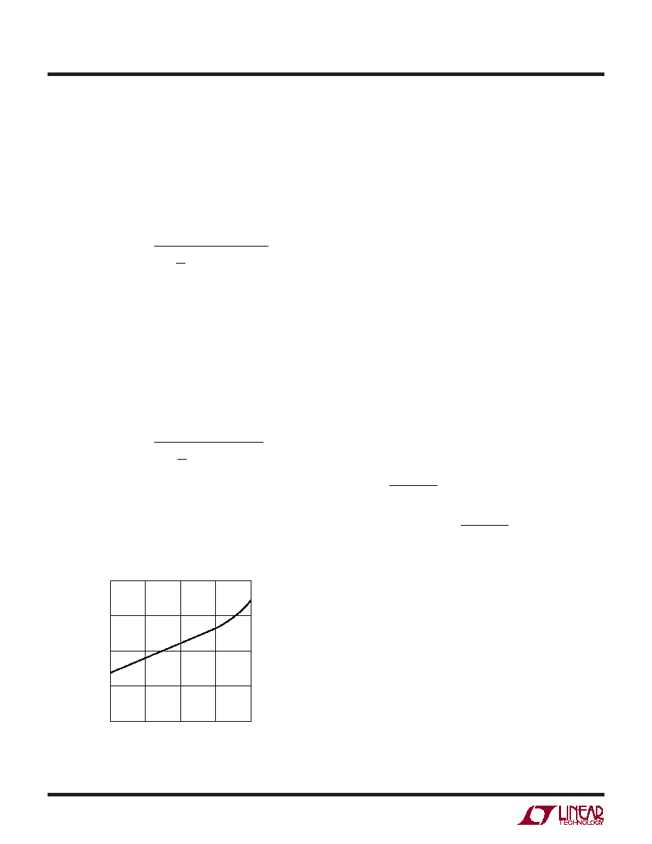
Programming the Operating Frequency
The choice of operating frequency and inductor value is a
tradeoff between efficiency and component size. Low
frequency operation improves efficiency by reducing
MOSFET and diode switching losses. However, lower
frequency operation requires more inductance for a given
amount of load current.
The LTC3783 uses a constant frequency architecture that
can be programmed over a 20kHz to 1MHz range with a
single external resistor from the FREQ pin to ground, as
shown in the application on the first page of this data
sheet. The nominal voltage on the FREQ pin is 0.615V, and
the current that flows out of the FREQ pin is used to charge
and discharge an internal oscillator capacitor. The oscil-
lator frequency is trimmed to 300kHz with R
T
= 20k. A
graph for selecting the value of R
T
for a given operating
frequency is shown in Figure 2.
OPERATIO
U
3783 F01
2V TO 7V
MODE/
SYNC
GATE
I
L
t
MIN
= 25ns
0.8T
D = 40%
T
T = 1/f
O
Figure 1. MODE/SYNC Clock Input and Switching Waveforms
for Synchronized Operation
Figure 2. Timing Resistor (R
T
) Value
FREQUENCY (kHz)
10
R
T
(k
)
100
1
100
1000
10000
3783 G09
1
10
1000
11
LTC3783
3783f
INTV
CC
Regulator Bypassing and Operation
An internal, P-channel low dropout voltage regulator pro-
duces the 7V supply which powers the gate drivers and
logic circuitry within the LTC3783 as shown in Figure 3.
The INTV
CC
regulator can supply up to 50mA and must be
bypassed to ground immediately adjacent to the IC pins
with a minimum of 4.7
µF low ESR or ceramic capacitor.
Good bypassing is necessary to supply the high transient
currents required by the MOSFET gate driver.
For input voltages that don't exceed 8V (the absolute
maximum rating for INTV
CC
is 9V), the internal low drop-
out regulator in the LTC3783 is redundant and the INTV
CC
pin can be shorted directly to the V
IN
pin. With the INTV
CC
pin shorted to V
IN
, however, the divider that programs the
regulated INTV
CC
voltage will draw 15
µA from the input
supply, even in shutdown mode. For applications that
require the lowest shutdown mode input supply current,
do not connect the INTV
CC
pin to V
IN
. Regardless of
whether the INTV
CC
pin is shorted to V
IN
or not, it is always
necessary to have the driver circuitry bypassed with a
4.7
µF low ESR ceramic capacitor to ground immediately
adjacent to the INTV
CC
and GND pins.
In an actual application, most of the IC supply current is
used to drive the gate capacitance of the power MOSFET.
As a result, high input voltage applications in which a large
power MOSFET is being driven at high frequencies can
cause the LTC3783 to exceed its maximum junction tem-
perature rating. The junction temperature can be esti-
mated using the following equations:
I
Q(TOT)
= I
Q
+ f ∑ Q
G
P
IC
= V
IN
∑ (I
Q
+ f ∑ Q
G
)
T
J
= T
A
+ P
IC
∑
JA
The total quiescent current I
Q(TOT)
consists of the static
supply current (I
Q
) and the current required to charge and
discharge the gate of the power MOSFET. The 16-lead FE
package has a thermal resistance of
JA
= 38
∞C/W and the
DHD package has an
JA
= 43
∞C/W
As an example, consider a power supply with V
IN
= 12V
and V
OUT
= 25V at I
OUT
= 1A. The switching frequency is
300kHz, and the maximum ambient temperature is 70
∞C.
The power MOSFET chosen is the Si7884DP, which has a
maximum R
DS(ON)
of 10m
(at room temperature) and a
OPERATIO
U
≠
+
1.230V
R2
R1
P-CH
7V
DRIVER
GATE
C
VCC
4.7
µF
X5R
C
IN
INPUT
SUPPLY
6V TO 36V
GND
PLACE AS CLOSE AS
POSSIBLE TO DEVICE PINS
M1
3783 F03
INTV
CC
V
IN
GND
LOGIC
6V-RATED
POWER
MOSFET
Figure 3. Bypassing the LDO Regulator and Gate Driver Supply

12
LTC3783
3783f
maximum total gate charge of 35nC (the temperature
coefficient of the gate charge is low).
I
Q(TOT)
= 1.2mA + 35nC ∑ 300kHz = 12mA
P
IC
= 12V ∑ 12mA = 144mW
T
J
= 70
∞C + 110∞C/W ∑ 144mW = 86∞C
This demonstrates how significant the gate charge current
can be when compared to the static quiescent current in
the IC.
To prevent the maximum junction temperature from being
exceeded, the input supply current must be checked when
operating in a continuous mode at high V
IN
. A tradeoff
between the operating frequency and the size of the power
MOSFET may need to be made in order to maintain a
reliable IC junction temperature. Prior to lowering the
operating frequency, however, be sure to check with the
power MOSFET manufacturers for the latest low Q
G
, low
R
DS(ON)
devices. Power MOSFET manufacturing tech-
nologies are continually improving, with newer and better-
performing devices being introduced almost monthly.
Output Voltage Programming
In constant voltage mode, in order to regulate the output
voltage, the output voltage is set by a resistor divider
according to the following formula:
V
V
R
R
OUT
FBP
=
+
∑ 1
2
1
where 0
V
FBP
1.23V. The external resistor divider is
connected to the output as shown in Figure 4, allowing
remote voltage sensing. The resistors R1 and R2 are
typically chosen so that the error caused by the 500nA
input bias current flowing out of the FBN pin during
normal operation is less than 1%, which translates to a
maximum R1 value of about 25k at V
FBP
= 1.23V. For
lower FBP voltages, R1 must be reduced accordingly to
maintain accuracy, e.g., R1 < 2k for 1% accuracy when
V
FBP
= 100mV. More accuracy can be achieved with lower
resistances, at the expense of increased dissipation and
decreased light load efficiency.
A similar analysis applies to the V
FBP
resistive divider, if
one is used:
V
V
R
R
R
FBP
REF
=
+
∑
3
3
4
where R3 is subject to a similar 500nA bias current.
OPERATIO
U
LTC3783
R4
R3
RUN
PWMIN
I
TH
SS
V
REF
FBP
FBN
FREQ
SYNC
V
IN
OV/FB
PWMOUT
I
LIM
GATE
SENSE
INTV
CC
GND
V
IN
3V TO 36V
GND
V
OUT
R2
R1
3783 F04
Figure 4. LTC3783 Boost Application
Programming Turn-On and Turn-Off Thresholds
with the RUN Pin
The LTC3783 contains an independent, micropower volt-
age reference and comparator detection circuit that re-
mains active even when the device is shut down, as shown
in Figure 5. This allows users to accurately program an
input voltage at which the converter will turn on and off.
The falling threshold on the RUN pin is equal to the internal
reference voltage of 1.248V. The comparator has 100mV
of hysteresis to increase noise immunity.
The turn-on and turn-off input voltage thresholds are
programed using a resistor divider according to the fol-
lowing formulas:
V
V
R
R
V
V
R
R
IN OFF
IN ON
(
)
(
)
.
∑
.
∑
=
+
=
+
1 248
1
2
1
1 348
1
2
1
The resistor R1 is typically chosen to be less than 1M.

13
LTC3783
3783f
For applications where the RUN pin is only to be used as
a logic input, the user should be aware of the 7V Absolute
Maximum Rating for this pin! The RUN pin can be con-
nected to the input voltage through an external 1M resis-
tor, as shown in Figure 5c, for "always on" operation.
Soft-Start Capacitor Selection
For proper soft-start operation, the LTC3783 should have
a sufficiently large soft-start capacitor, C
SS
, attached to
the SS pin. The minimum soft-start capacitor size can be
estimated on the basis of output voltage, capacitor size
and load current. In addition, PWM operation reduces the
effective SS capacitor value by the dimming ratio.
C
g ratio
A C
V
R
mV
V
SS MIN
OUT
OUT
DS ON SENSE
(
)
(
)/
∑ dimmin
∑
∑
∑
∑
∑ .
>
µ
2
50
150
1 2
assuming 50% ripple current, where R
DS(ON)/SENSE
repre-
sents either the R
DS(ON)
of the switching MOSFET or
R
SENSE
, whichever is used on the SENSE pin. Dimming
ratio is described by 1/D
PWM
as shown in Figure 6.
Application Circuits
A basic LTC3783 PWM-dimming LED application is shown
on the first page of this data sheet.
Operating Frequency and PWM Dimming Ratio
The minimum operating frequency, f
OSC
, required for
proper operation of a PWM dimming application depends
on the minimum PWM frequency, f
PWM
, the dimming ratio
1/D
PWM
, and N, the number of f
OSC
cycles per PWM cycle:
f
N f
D
OSC
PWM
PWM
>
∑
OPERATIO
U
Figure 5a. Programming the Turn-On and Turn-Off Thresholds Using the RUN Pin
Figure 5b. On/Off Control Using External Logic
Figure 5c. External Pull-Up Resistor on
RUN Pin for "Always On" Operation
≠
+
RUN
COMPARATOR
V
IN
RUN
R2
R1
INPUT
SUPPLY
OPTIONAL
FILTER
CAPACITOR
+
≠
GND
3783 F05a
BIAS AND
START-UP
CONTROL
1.248V
µPOWER
REFERENCE
6V
≠
+
RUN
COMPARATOR
1.248V
3483 F05b
RUN
6V
EXTERNAL
LOGIC CONTROL
≠
+
RUN
COMPARATOR
V
IN
RUN
R2
1M
INPUT
SUPPLY
+
≠
GND
1.248V
3483 F05c
6V

14
LTC3783
3783f
Figure 6 illustrates these various quantities in relation to
one another.
Typically, in order to avoid visible flicker, f
PWM
should be
greater than 120Hz. Assuming inductor and capacitor
sizing which is close to discontinuous operation, 2 f
OSC
cycles are sufficient for proper PWM operation. Thus,
within the 1MHz rated maximum f
OSC
, a dimming ratio of
1/D
PWM
= 3000 is possible.
output current needs to be reflected back to the input in
order to dimension the power MOSFET properly. Based on
the fact that, ideally, the output power is equal to the input
power, the maximum average input current is:
I
I
D
IN MAX
OUT MAX
MAX
(
)
(
)
≠
=
1
The peak input current is:
I
I
D
IN PEAK
OUT MAX
MAX
(
)
(
)
∑
≠
= +
1
2
1
The maximum duty cycle, D
MAX
, should be calculated at
minimum V
IN
.
Boost Converter: Ripple Current
I
L
and the `' Factor
The constant `' in the equation above represents the
percentage peak-to-peak ripple current in the inductor,
relative to its maximum value. For example, if 30% ripple
current is chosen, then = 0.3, and the peak current is
15% greater than the average.
For a current mode boost regulator operating in CCM,
slope compensation must be added for duty cycles above
50% in order to avoid subharmonic oscillation. For the
LTC3783, this ramp compensation is internal. Having an
internally fixed ramp compensation waveform, however,
does place some constraints on the value of the inductor
and the operating frequency. If too large an inductor is
used, the resulting current ramp (
I
L
) will be small relative
to the internal ramp compensation (at duty cycles above
50%), and the converter operation will approach voltage
mode (ramp compensation reduces the gain of the current
loop). If too small an inductor is used, but the converter is
still operating in CCM (near critical conduction mode), the
internal ramp compensation may be inadequate to prevent
subharmonic oscillation. To ensure good current mode
gain and to avoid subharmonic oscillation, it is recom-
mended that the ripple current in the inductor fall in the
range of 20% to 40% of the maximum average current. For
example, if the maximum average input current is 1A,
choose a
I
L
between 0.2A and 0.4A, and correspondingly
a value `' between 0.2 and 0.4.
OPERATIO
U
Figure 6. PWM Dimming Parameters
PWMIN
GATE
3783 F06
# = N
D
PWM
/f
PWM
1/f
PWM
1/f
OSC
Boost Converter: Duty Cycle Considerations
For a boost converter operating in a continuous conduc-
tion mode (CCM), the duty cycle of the main switch is:
D
V
V
V
V
V
OUT
D
IN
OUT
D
=
+
+
≠
where V
D
is the forward voltage of the boost diode. For
converters where the input voltage is close to the output
voltage, the duty cycle is low, and for converters that
develop a high output voltage from a low input voltage, the
duty cycle is high. The maximum output voltage for a
boost converter operating in CCM is:
V
V
D
V
OUT MAX
IN MIN
MAX
D
(
)
(
)
≠
≠
=
1
The maximum duty cycle capability of the LTC3783 is
typically 90%. This allows the user to obtain high output
voltages from low input supply voltages.
Boost Converter: The Peak and Average Input Currents
The control circuit in the LTC3783 is measuring the input
current (either by using the R
DS(ON)
of the power MOSFET
or by using a sense resistor in the MOSFET source), so the
15
LTC3783
3783f
Boost Converter: Inductor Selection
Given an operating input voltage range, and having chosen
the operating frequency and ripple current in the inductor,
the inductor value can be determined using the following
equation:
L
V
I
f
D
where
I
I
IN MIN
L
MAX
L
OUT
=
=
(
)
(
∑
∑
:
∑
M
MAX
MAX
D
)
≠
1
Remember that most boost converters are not short-
circuit protected. Under a shorted output condition, the
inductor current is limited only by the input supply capa-
bility. For applications requiring a step-up converter that is
short-circuit protected, please refer to the applications
section covering SEPIC converters.
The minimum required saturation current of the inductor
can be expressed as a function of the duty cycle and the
load current, as follows:
I
I
D
L SAT
OUT MAX
MAX
(
)
(
)
∑
≠
> +
1
2
1
The saturation current rating for the inductor should be
checked at the minimum input voltage (which results in the
highest inductor current) and maximum output current.
Boost Converter: Operating in Discontinuous Mode
Discontinuous mode operation occurs when the load
current is low enough to allow the inductor current to run
out during the off-time of the switch, as shown in Figure 7.
Once the inductor current is near zero, the switch and
diode capacitances resonate with the inductance to form
damped ringing at 1MHz to 10MHz. If the off-time is long
enough, the drain voltage will settle to the input voltage.
Depending on the input voltage and the residual energy in
the inductor, this ringing can cause the drain of the power
MOSFET to go below ground where it is clamped by the
body diode. This ringing is not harmful to the IC and it has
not been shown to contribute significantly to EMI. Any
attempt to damp it with a snubber will degrade the
efficiency.
Boost Converter: Power MOSFET Selection
The power MOSFET can serve two purposes in the LTC3783:
it represents the main switching element in the power
path, and its R
DS(ON)
can represent the current sensing
element for the control loop. Important parameters for the
power MOSFET include the drain-to-source breakdown
voltage BV
DSS
, the threshold voltage V
GS(TH)
, the on-
resistance R
DS(ON)
versus gate-to-source voltage, the
gate-to-source and gate-to-drain charges Q
GS
and Q
GD
,
respectively, the maximum drain current I
D(MAX)
and the
MOSFET's thermal resistances
JC
and
JA
.
The gate drive voltage is set by the 7V INTV
CC
low drop
regulator. Consequently, 6V rated MOSFETs are required
in most high voltage LTC3783 applications. If low input
voltage operation is expected (e.g., supplying power from
a lithium-ion battery or a 3.3V logic supply), then sublogic-
level threshold MOSFETs should be used. Pay close atten-
tion to the BV
DSS
specifications for the MOSFETs relative
to the maximum actual switch voltage in the application.
Many logic-level devices are limited to 30V or less, and the
switch node can ring during the turn-off of the MOSFET
due to layout parasitics. Check the switching waveforms
of the MOSFET directly across the drain and source
terminals using the actual PC board layout for excessive
ringing.
OPERATIO
U
OUTPUT
VOLTAGE
200mV/DIV
INDUCTOR
CURRENT
1A/DIV
1
µs/DIV
3783 F07
MOSFET
DRAIN
VOLTAGE
20V/DIV
Figure 7. Discontinuous Mode Waveforms
16
LTC3783
3783f
During the switch on-time, the IMAX comparator limits the
absolute maximum voltage drop across the power
MOSFET to a nominal 150mV, regardless of duty cycle.
The peak inductor current is therefore limited to
150mV/R
DS(ON)
. The relationship between the maximum
load current, duty cycle, and the R
DS(ON)
of the power
MOSFET is:
R
mV
D
I
DS ON
MAX
OUT MAX
T
(
)
(
)
∑
≠
∑
∑
<
+
150
1
1
2
The
T
term accounts for the temperature coefficient of the
R
DS(ON)
of the MOSFET, which is typically 0.4%/
∞C. Fig-
ure 8 illustrates the variation of normalized R
DS(ON)
over
temperature for a typical power MOSFET.
Another method of choosing which power MOSFET to use
is to check what the maximum output current is for a given
R
DS(ON)
, since MOSFET on-resistances are available in
discrete values.
I
mV
D
R
O MAX
MAX
DS ON
T
(
)
(
)
∑
≠
∑
∑
=
+
150
1
1
2
It is worth noting that the 1 - D
MAX
relationship between
I
O(MAX)
and R
DS(ON)
can cause boost converters with a
wide input range to experience a dramatic range of maxi-
mum input and output currents. This should be taken into
consideration in applications where it is important to limit
the maximum current drawn from the input supply, and
also to avoid triggering the 150mV IMAX comparator, as
this condition can result in excessive noise.
Calculating Power MOSFET Switching and Conduction
Losses and Junction Temperatures
In order to calculate the junction temperature of the power
MOSFET, the power dissipated by the device must be
known. This power dissipation is a function of the duty
cycle, the load current, and the junction temperature itself
(due to the positive temperature coefficient of its R
DS(ON)
).
As a result, some iterative calculation is normally required
to determine a reasonably accurate value. Since the con-
troller is using the MOSFET as both a switching and a
sensing element, care should be taken to ensure that the
converter is capable of delivering the required load current
over all operating conditions (line voltage and tempera-
ture), and for the worst-case specifications for V
SENSE(MAX)
and the R
DS(ON)
of the MOSFET listed in the manufacturer's
data sheet.
The power dissipated by the MOSFET in a boost converter
is:
P
I
D
R
D
k V
I
D
C
f
FET
OUT MAX
MAX
DS ON
MAX
T
OUT
OUT MAX
MAX
RSS
=
+
(
)
(
)
.
(
)
≠
∑
∑
∑
∑
∑
≠
∑
∑
1
1
2
1 85
The first term in the equation above represents the I
2
R
losses in the device, and the second term, the switching
losses. The constant k = 1.7 is an empirical factor inversely
related to the gate drive current and has the dimension of
1/current.
From a known power dissipated in the power MOSFET, its
junction temperature can be obtained using the following
formula:
T
J
= T
A
+ P
FET
∑
JA
The
JA
to be used in this equation normally includes the
JC
for the device plus the thermal resistance from the
case to the ambient temperature (
CA
). This value of T
J
can
then be compared to the original, assumed value used in
the iterative calculation process.
OPERATIO
U
JUNCTION TEMPERATURE (
∞C)
≠ 50
T
NORMALIZED ON RESISTANCE
1.0
1.5
150
3783 F08
0.5
0
0
50
100
2.0
Figure 8. Normalized R
DS(ON)
vs Temperature
17
LTC3783
3783f
Boost Converter: Output Diode Selection
To maximize efficiency, a fast switching diode with low
forward drop and low reverse leakage is desired. The
output diode in a boost converter conducts current during
the switch off-time. The peak reverse voltage that the
diode must withstand is equal to the regulator output
voltage. The average forward current in normal operation
is equal to the output current, and the peak current is equal
to the peak inductor current.
I
I
I
D
D PEAK
L PEAK
OUT MAX
MA
(
)
(
)
(
)
∑
≠
=
= +
1
2
1
X
X
The power dissipated by the diode is:
P
D
= I
OUT(MAX)
∑ V
D
and the diode junction temperature is:
T
J
= T
A
+ P
D
∑
JA
The
JA
to be used in this equation normally includes the
JC
for the device plus the thermal resistance from the
board to the ambient temperature in the enclosure.
Remember to keep the diode lead lengths short and to
observe proper switch-node layout (see Board Layout
Checklist) to avoid excessive ringing and increased
dissipation.
Boost Converter: Output Capacitor Selection
Contributions of ESR (equivalent series resistance), ESL
(equivalent series inductance) and the bulk capacitance
must be considered when choosing the correct compo-
nent for a given output ripple voltage. The effects of these
three parameters (ESR, ESL and bulk C) on the output
voltage ripple waveform are illustrated in Figure 9 for a
typical boost converter.
The choice of component(s) begins with the maximum
acceptable ripple voltage (expressed as a percentage of
the output voltage), and how this ripple should be divided
between the ESR step and the charging/discharging
V.
For the purpose of simplicity we will choose 2% for the
maximum output ripple, to be divided equally between the
ESR step and the charging/discharging
V. This percent-
age ripple will change, depending on the requirements of
the application, and the equations provided below can
easily be modified.
For a 1% contribution to the total ripple voltage, the ESR
of the output capacitor can be determined using the
following equation:
ESR
V
I
where
I
COUT
OUT
IN PEAK
IN PEAK
<
=
0 01
1
.
∑
:
(
)
(
)
+
+
2
1
∑
≠
(
)
I
D
OUT MAX
MAX
For the bulk C component, which also contributes 1% to
the total ripple:
C
I
V
f
OUT
OUT MAX
OUT
>
(
)
.
∑
∑
0 01
For many designs it is possible to choose a single capaci-
tor type that satisfies both the ESR and bulk C require-
ments for the design. In certain demanding applications,
however, the ripple voltage can be improved significantly
by connecting two or more types of capacitors in parallel.
For example, using a low ESR ceramic capacitor can
minimize the ESR setup, while an electrolytic capacitor
can be used to supply the required bulk C.
Once the output capacitor ESR and bulk capacitance have
been determined, the overall ripple voltage waveform
should be verified on a dedicated PC board (see Board
OPERATIO
U
V
OUT
(AC)
V
ESR
RINGING DUE TO
TOTAL INDUCTANCE
(BOARD + CAP)
V
COUT
3783 F09
Figure 9. Output Ripple Voltage

18
LTC3783
3783f
Layout section for more information on component place-
ment). Lab breadboards generally suffer from excessive
series inductance (due to inter-component wiring), and
these parasitics can make the switching waveforms look
significantly worse than they would be on a properly
designed PC board.
The output capacitor in a boost regulator experiences high
RMS ripple currents. The RMS output capacitor ripple
current is:
I
I
V
V
V
RMS COUT
OUT MAX
OUT
IN MIN
IN MIN
(
)
(
)
(
)
(
)
∑
≠
Note that the ripple current ratings from capacitor manu-
facturers are often based on only 2000 hours of life. This
makes it advisable to further derate the capacitor or to
choose a capacitor rated at a higher temperature than
required. Several capacitors may also be placed in parallel
to meet size or height requirements in the design.
Boost Converter: Input Capacitor Selection
The input capacitor of a boost converter is less critical than
the output capacitor, due to the fact that the inductor is in
series with the input, and hence, the input current wave-
form is continuous (see Figure 10). The input voltage
source impedance determines the size of the input capaci-
tor, which is typically in the range of 10
µF to 100µF. A low
ESR capacitor is recommended, although it is not as
critical as for the output capacitor.
The RMS input capacitor ripple current for a boost con-
verter is:
I
V
L f
D
RMS CIN
IN MIN
MAX
(
)
(
)
. ∑
∑
∑
0 3
Please note that the input capacitor can see a very high
surge current when a battery is suddenly connected to the
input of the converter, and solid tantalum capacitors can
fail catastrophically under these conditions. Be sure to
specify surge-tested capacitors!
Boost Converter Design Example
The design example given here will be for the circuit shown
in Figure 1. The input voltage is 12V, and the output voltage
is 25V at a maximum load current of 0.7A (1A peak).
1. The duty cycle is:
D
V
V
V
V
V
OUT
D
IN
OUT
D
=
+
+
=
+
+
=
≠
. ≠
.
%
25 0 4 12
25 0 4
53
2. The operating frequency is chosen to be 1MHz to
maximize the PWM dimming range. From Figure 2, the
resistor from the FREQ pin to ground is 6k.
3. An inductor ripple current of 40% of the maximum load
current is chosen, so the peak input current (which is also
the minimum saturation current) is:
I
I
D
IN PEAK
OUT MAX
MAX
(
)
(
)
∑
≠
. ∑
.
= +
=
1
2
1
1 2
0
7
7
1 0 53
1 8
≠ .
.
=
A
The inductor ripple current is:
=
-
=
-
=
IL
OUT MAX
MAX
I
D
A
∑
. ∑
.
.
.
(
)
1
0 4
0 7
1 0 53
0 6
And so the inductor value is:
L
V
I
f
D
V
A
MHz
µH
IN MIN
L
MAX
=
=
=
(
)
∑
∑
.
∑
∑ .
12
0 6
1
0 53
11
4. R
SENSE
should be:
R
V
I
mV
SENSE
SENSE MAX
IN PEAK
=
=
0 5
0 5 150
1
. ∑
. ∑
.
(
)
(
)
8
8
42
A
m
=
OPERATIO
U
I
IN
I
L
Figure 10. Inductor and Input Currents

19
LTC3783
3783f
OPERATIO
U
5. The diode for this design must handle a maximum DC
output current of 0.7A and be rated for a minimum reverse
voltage of V
OUT
, or 25V. A 1A, 40V diode from Zetex was
chosen for its specifications, especially low leakage at
higher temperatures, which is important for maintaining
dimming range.
6. Voltage and value permitting, the output capacitor
usually consists of some combination of low ESR ceram-
ics. Based on a maximum output ripple voltage of 1%, or
250mV, the bulk C needs to be greater than:
C
I
V
f
A
V
MHz
OUT
OUT MAX
OUT
>
=
(
)
.
∑
∑
.
.
∑
∑
0 01
0 7
0 01 25
1
=
= µ
3 F
The RMS ripple current rating for this capacitor needs to
exceed:
I
I
V
V
V
RMS COUT
OUT MAX
OUT
IN MIN
IN MIN
(
)
(
)
(
)
(
)
∑
≠
=
= 00 7
25
12
12
0 7
.
∑
≠
.
A
V
V
V
A
=
Based on value and ripple current, and taking physical size
into account, a surface mount ceramic capacitor is a good
choice. A 4.7
µF TDK C5750X7R1H475M will satisfy all
requirements in a compact package.
7. The soft-start capacitor should be:
C
g ratio
A C
V
R
SS MIN
OUT
OUT
DS
(
)
(
∑ dimmin
∑
∑
∑
∑
>
µ
2
50
O
ON SENSE
mV
V
A
F
V
)/
∑ .
∑
∑
∑ .
∑
∑
150
1 2
2 3000 50
4 7
25
>
µ
µ
4
42
150
1 2
8
m
mV
V
F
= µ
∑ .
8. The choice of an input capacitor for a boost converter
depends on the impedance of the source supply and the
amount of input ripple the converter will safely tolerate.
For this particular design and lab setup, 20
µF was found to
be satisfactory.
PC Board Layout Checklist
1. In order to minimize switching noise and improve
output load regulation, the GND pad of the LTC3783
should be connected directly to 1) the negative terminal of
the INTV
CC
decoupling capacitor, 2) the negative terminal
of the output decoupling capacitors, 3) the bottom termi-
nals of the sense resistors or the source of the power
MOSFET, 4) the negative terminal of the input capacitor,
and 5) at least one via to the ground plane immediately
under the exposed pad. The ground trace on the top layer
of the PC board should be as wide and short as possible
to minimize series resistance and inductance.
2. Beware of ground loops in multiple layer PC boards. Try
to maintain one central ground node on the board and use
the input capacitor to avoid excess input ripple for high
output current power supplies. If the ground plane is to be
used for high DC currents, choose a path away from the
small-signal components.
3. Place the C
VCC
capacitor immediately adjacent to the
INTV
CC
and GND pins on the IC package. This capacitor
carries high di/dt MOSFET gate-drive currents. A low ESR
and ESL 4.7
µF ceramic capacitor works well here.
4. The high di/dt loop from the bottom terminal of the
output capacitor, through the power MOSFET, through the
boost diode and back through the output capacitors should
be kept as tight as possible to reduce inductive ringing.
Excess inductance can cause increased stress on the
power MOSFET and increase HF noise on the output. If low
ESR ceramic capacitors are used on the output to reduce
output noise, place these capacitors close to the boost
diode in order to keep the series inductance to a minimum.
5. Check the stress on the power MOSFET by measuring
its drain-to-source voltage directly across the device ter-
minals (reference the ground of a single scope probe
directly to the source pad on the PC board). Beware of
inductive ringing which can exceed the maximum speci-
fied voltage rating of the MOSFET. If this ringing cannot be
avoided and exceeds the maximum rating of the device,
either choose a higher voltage device or specify an ava-
lanche-rated power MOSFET.
6. Place the small-signal components away from high
frequency switching nodes. All of the small-signal compo-
nents should be placed on one side of the IC and all of the
power components should be placed on the other. This
also allows the use of a pseudo-Kelvin connection for the
signal ground, where high di/dt gate driver currents flow

20
LTC3783
3783f
out of the IC ground pad in one direction (to bottom plate
of the INTV
CC
decoupling capacitor) and small-signal
currents flow in the other direction.
7. If a sense resistor is used in the source of the power
MOSFET, minimize the capacitance between the SENSE
pin trace and any high frequency switching nodes. The
LTC3783 contains an internal leading-edge blanking time
of approximately 160ns, which should be adequate for
most applications.
8. For optimum load regulation and true remote sensing,
the top of the output resistor should connect indepen-
dently to the top of the output capacitor (Kelvin connec-
tion), staying away from any high dV/dt traces. Place the
divider resistors near the LTC3783 in order to keep the
high impedance FBN node short.
9. For applications with multiple switching power convert-
ers connected to the same input supply, make sure that the
input filter capacitor for the LTC3783 is not shared with
any other converters. AC input current from another
converter could cause substantial input voltage ripple, and
this could interfere with the operation of the LTC3783. A
few inches of PC trace or wire (L ~ 100nH) between the C
IN
of the LTC3783 and the actual source V
IN
should be
sufficient to prevent current-sharing problems.
Returning the Load to V
IN
: A Single Inductor
Buck-Boost Application
As shown in Figure 11, due to its available high side
current sensing mode, the LTC3783 is also well-suited to
a boost converter in which the load current is returned to
V
IN
, hence providing a load voltage (V
OUT
≠ V
IN
) which can
be greater or less than the input voltage V
IN
. This configu-
ration allows for complete overlap of input and output
voltages, with the disadvantages that only the load cur-
rent, and not the load voltage, can be tightly regulated. The
switch must be rated for a V
DS(MAX)
equal to V
IN
+ V
LOAD
.
The design of this circuit resembles that of the boost
converter above, and the procedure is much the same,
except V
OUT
is now (V
IN
+ V
LOAD
), and the duty cycles and
voltages must be adjusted accordingly.
Similar to the boost converter, which can be dimmed via
the digital PWMIN input or the analog FBP pin, the buck-
boost can be dimmed via the PWMIN pin or the analog
I
LIM
pin, which adjusts the offset voltage to which the
loop will drive (V
FBP
≠ V
FBN
). In the case of the buck-
boost, however, the dimming ratio cannot be as high as
in the boost converter, since there is no load switch to
preserve the V
OUT
level while PWMIN is low.
OPERATIO
U
Figure 11. Single Inductor Buck-Boost Application with Analog Dimming and Low Frequency PWM Dimming
LTC3783
RUN
PWMIN
I
TH
SS
V
REF
FBP
FBN
FREQ
SYNC
V
IN
OV/FB
PWMOUT
I
LIM
GATE
SENSE
INTV
CC
GND
V
IN
9V TO 26V
R
L
0.28
V
OUT
LED STRING 1-4 EA
LUMILEDS LHXL-BW02
EACH LED IS 3V TO 4.2V
AT 350mA
10
µF, 50V
C5750X7R1H106M
CERAMIC
0V TO
1.23V
10
µF, 50V
◊2
UMK432C106MM
10
µH
SUMIDA
CDRH8D28-100
GND
3783 F11
1M
20k
PMEG6010
FAIRCHILD
FDN5630
1k
40.2k
4.7
µF
100k
PWM
5V AT 0Hz TO 10Hz
4.7
µF
0.05
1
µF
21
LTC3783
3783f
OPERATIO
U
Figure 12. LED Buck Application
Using the LTC3783 for Buck Applications
As shown in Figure 12, high side current sensing also
allows the LTC3783 to control a functional buck con-
verter when load voltage is always sufficiently less than
V
IN
. In this scheme the input voltage to the inductor is
lowered by the load voltage. The boost converter now
sees a V
IN
' = V
IN
≠ V
LOAD
, meaning the controller is now
boosting from (V
IN
≠ V
LOAD
) to V
IN
.
LTC3783
RUN
PWMIN
I
TH
SS
V
REF
FBP
FBN
FREQ
SYNC
V
IN
OV/FB
PWMOUT
I
LIM
GATE
SENSE
INTV
CC
GND
V
IN
6V TO 36V
LED STRING
GND
3783 F12

22
LTC3783
3783f
U
PACKAGE DESCRIPTIO
DHD Package
16-Lead Plastic DFN (5mm
◊ 4mm)
(Reference LTC DWG # 05-08-1707)
4.00
±0.10
(2 SIDES)
5.00
±0.10
(2 SIDES)
NOTE:
1. DRAWING PROPOSED TO BE MADE VARIATION OF VERSION (WJGD-2) IN JEDEC
PACKAGE OUTLINE MO-229
2. DRAWING NOT TO SCALE
3. ALL DIMENSIONS ARE IN MILLIMETERS
4. DIMENSIONS OF EXPOSED PAD ON BOTTOM OF PACKAGE DO NOT INCLUDE
MOLD FLASH. MOLD FLASH, IF PRESENT, SHALL NOT EXCEED 0.15mm ON ANY SIDE
5. EXPOSED PAD SHALL BE SOLDER PLATED
6. SHADED AREA IS ONLY A REFERENCE FOR PIN 1 LOCATION ON THE
TOP AND BOTTOM OF PACKAGE
0.40
± 0.10
BOTTOM VIEW--EXPOSED PAD
2.44
± 0.10
(2 SIDES)
0.75
±0.05
R = 0.115
TYP
R = 0.20
TYP
4.34
±0.10
(2 SIDES)
1
8
16
9
PIN 1
TOP MARK
(SEE NOTE 6)
0.200 REF
0.00 ≠ 0.05
(DHD16) DFN 0504
0.25
± 0.05
PIN 1
NOTCH
0.50 BSC
4.34
±0.05
(2 SIDES)
RECOMMENDED SOLDER PAD PITCH AND DIMENSIONS
2.44
±0.05
(2 SIDES)
3.10
±0.05
0.50 BSC
0.70
±0.05
4.50
±0.05
PACKAGE
OUTLINE
0.25
± 0.05
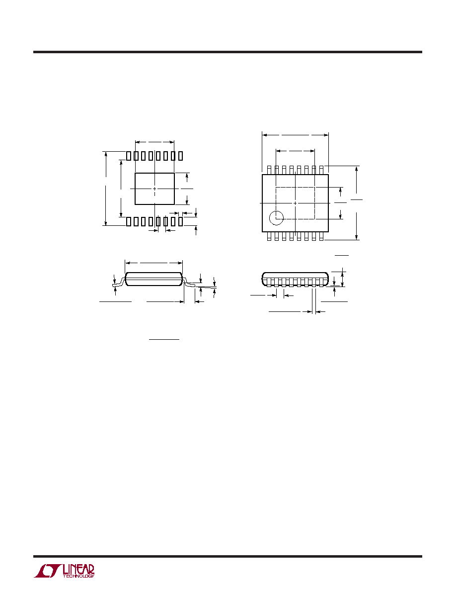
23
LTC3783
3783f
Information furnished by Linear Technology Corporation is believed to be accurate and reliable.
However, no responsibility is assumed for its use. Linear Technology Corporation makes no represen-
tation that the interconnection of its circuits as described herein will not infringe on existing patent rights.
U
PACKAGE DESCRIPTIO
FE Package
16-Lead Plastic TSSOP (4.4mm)
(Reference LTC DWG # 05-08-1663)
Exposed Pad Variation BC
FE16 (BC) TSSOP 0204
0.09 ≠ 0.20
(.0035 ≠ .0079)
0
∞ ≠ 8∞
0.25
REF
0.50 ≠ 0.75
(.020 ≠ .030)
4.30 ≠ 4.50*
(.169 ≠ .177)
1
3
4
5
6 7 8
10
9
4.90 ≠ 5.10*
(.193 ≠ .201)
16 1514 13 12 11
1.10
(.0433)
MAX
0.05 ≠ 0.15
(.002 ≠ .006)
0.65
(.0256)
BSC
2.94
(.116)
0.195 ≠ 0.30
(.0077 ≠ .0118)
TYP
2
RECOMMENDED SOLDER PAD LAYOUT
0.45
±0.05
0.65 BSC
4.50
±0.10
6.60
±0.10
1.05
±0.10
2.94
(.116)
3.58
(.141)
3.58
(.141)
MILLIMETERS
(INCHES)
*DIMENSIONS DO NOT INCLUDE MOLD FLASH. MOLD FLASH
SHALL NOT EXCEED 0.150mm (.006") PER SIDE
NOTE:
1. CONTROLLING DIMENSION: MILLIMETERS
2. DIMENSIONS ARE IN
3. DRAWING NOT TO SCALE
SEE NOTE 4
4. RECOMMENDED MINIMUM PCB METAL SIZE
FOR EXPOSED PAD ATTACHMENT
6.40
(.252)
BSC
24
LTC3783
3783f
© LINEAR TECHNOLOGY CORPORATION 2005
LT 1105 ∑ PRINTED IN THE USA
PART NUMBER
DESCRIPTION
COMMENTS
LT
Æ
1618
Monolithic 1.4MHz Boost Regulator
Constant-Current/Constant-Voltage, 1A Switch
LTC1871
Boost, Flyback, SEPIC Controller
No R
SENSE
, 2.5V
V
IN
36V, 92% Duty Cycle
LT3477
3A DC/DC LED Driver with Rail-to-Rail Current Sense
2.5V
V
IN
25V: Buck, Buck-Boost and Boost Topologies
LTC3780
High Power Buck-Boost Controller
4-Switch, 4V
V
IN
36V, 0.8V V
OUT
30V
LTC3782
2-Phase Boost Controller
High Power, 6V
V
IN
40V, 150kHz to 500kHz
LTC3827/LTC3827-1 Low I
Q
Current Dual Controllers
2-Phase, 80
µA I
Q
, 0.8V
V
OUT
10V, 4V V
IN
36V
LTC4002
Standalone 2A Li-Ion Battery Charger
1- and 2-Cell, 4.7V
V
IN
22V, 3 Hour Timer
RELATED PARTS
Linear Technology Corporation
1630 McCarthy Blvd., Milpitas, CA 95035-7417
(408) 432-1900
FAX: (408) 434-0507
www.linear.com