 | ÐлекÑÑоннÑй компоненÑ: LTC4214 | СкаÑаÑÑ:  PDF PDF  ZIP ZIP |
421412i.pm6
LTC4214-1/LTC4214-2
1
421412i
The LTC
®
4214 negative voltage Hot Swap
TM
controller
allows a board to be safely inserted and removed from a
live backplane. Output current is controlled by three stages
of current limiting: a timed circuit breaker, active current
limiting and a fast feedforward path that limits peak
current under worst-case catastrophic fault conditions.
Adjustable undervoltage and overvoltage detectors dis-
connect the load whenever the input supply exceeds the
desired operating range. The LTC4214 allows operation
with (V
IN
V
EE
) supplies ranging from 6V to 16V. A
multifunction timer delays initial start-up and controls the
circuit breaker's response time. This response time is
accelerated by sensing excessive MOSFET drain voltage,
keeping the MOSFET within its safe operating area (SOA).
An adjustable soft-start circuit controls MOSFET inrush
current at start-up. A power good status output can enable
a power module at start-up or disable it if the circuit
breaker trips.
The LTC4214-1 latches off after a circuit breaker fault times
out. The LTC4214-2 provides automatic retry after a fault.
The LTC4214 is available in the 10-pin MSOP.
s
Hot Board Insertion
s
Electronic Circuit Breaker
s
Negative Power Supply Control
s
Central Office Switching
s
Adjustable Current Limiting Circuit
s
High Availability Servers
s
Disk Arrays
, LTC and LT are registered trademarks of Linear Technology Corporation.
s
Allows Safe Board Insertion and Removal from a
Live Backplane
s
Operates from 6V to 16V
s
Adjustable Analog Current Limit With Circuit
Breaker Timer
s
Fast Response Time Limits Peak Fault Current
s
Adjustable Soft-Start Current Limit
s
Adjustable Timer with Drain Voltage Accelerated
Response
s
Adjustable Undervoltage/Overvoltage Protection
s
LTC4214-1: Latch Off After Fault
s
LTC4214-2: Automatic Retry After Fault
Negative Voltage
Hot Swap Controllers
November 2002
Hot Swap is a trademark of Linear Technology Corporation.
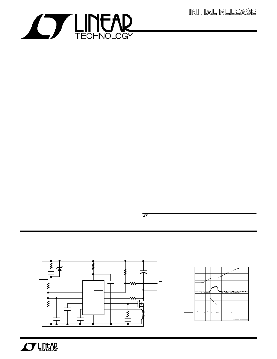
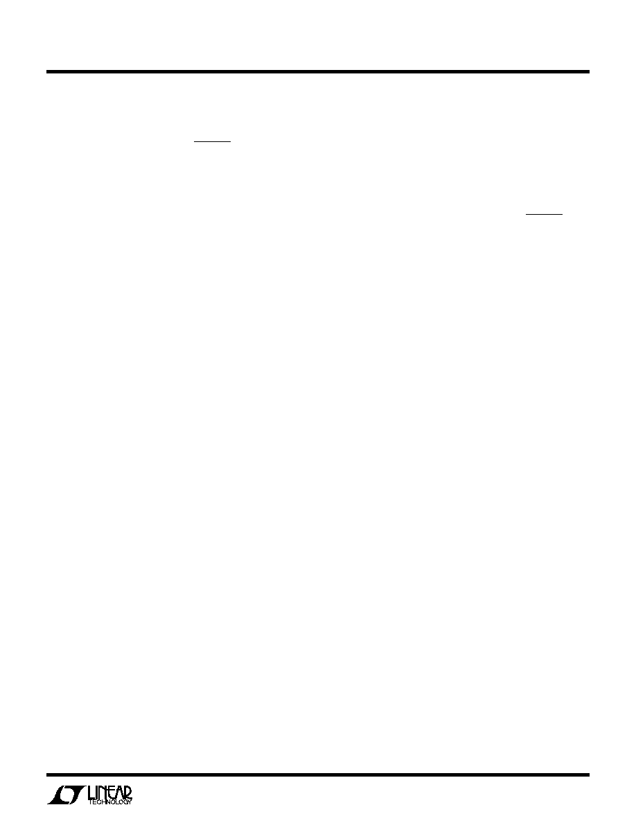
12V/2A Hot Swap Controller
4214 TA01
GND
OV
UV
V
EE
V
IN
SENSE
SS
TIMER
GATE
PWRGD
DRAIN
LTC4214-1
R1
121k
1%
R
X
10
R
IN
470
Z1
C
X
100nF
R2
32.4k
1%
C
T
47nF
C
SS
22nF
C
C
10nF
12V
R
S
0.025
Q1
IRF7413
V
OUT
GND
R
C
10
R3
10k
1
8
9
10
3
2
7
6
4
5
C1
1nF
C
IN
0.1
µ
F
C
L
100
µ
F
GND
(SHORT PIN)
+
R
D
475k
R4
10k
EN
Z1:SMAJ15A
Start-Up Behavior
FEATURES
DESCRIPTIO
U
APPLICATIO S
U
TYPICAL APPLICATIO
U
Final Electrical Specifications
Information furnished by Linear Technology Corporation is believed to be accurate and reliable.
However, no responsibility is assumed for its use. Linear Technology Corporation makes no represen-
tation that the interconnection of its circuits as described herein will not infringe on existing patent rights.
GATE
5V/DIV
SENSE
50mV/DIV
V
OUT
10V/DIV
PWRGD
10V/DIV
4214 TA02
LTC4214-1/LTC4214-2
2
421412i
SYMBOL
PARAMETER
CONDITIONS
MIN
TYP
MAX
UNITS
V
IN
Supply Voltage
q
6
16
V
I
IN
V
IN
Supply Current
UV = OV = 2.5V
q
0.8
2
mA
V
LKO
V
IN
Undervoltage Lockout
Coming Out of UVLO (Rising V
IN
)
q
5.1
5.6
V
V
LKH
V
IN
Undervoltage Lockout Hysteresis
0.3
V
V
CB
Circuit Breaker Current Limit Voltage
V
CB
= (V
SENSE
V
EE
)
q
44
50
56
mV
V
ACL
Analog Current Limit Voltage
V
ACL
= (V
SENSE
V
EE
), SS = Open
q
60
70
80
mV
V
FCL
Fast Current Limit Voltage
V
FCL
= (V
SENSE
V
EE
)
q
150
200
300
mV
V
SS
SS Voltage
After End of SS Timing Cycle
1.6
V
R
SS
SS Output Impedance
73
k
I
SS
SS Pin Current
UV = OV = 2.5V, V
SENSE
= V
EE
, V
SS
= 0V (Sourcing)
22
µ
A
UV = OV = 0V, V
SENSE
= V
EE
, V
SS
= 1V (Sinking)
28
mA
V
OS
Analog Current Limit Offset Voltage
10
mV
V
ACL
+V
OS
Ratio (V
ACL
+ V
OS
) to SS Voltage
0.05
V/V
V
SS
I
GATE
GATE Pin Output Current
V
SENSE
= V
EE
, V
GATE
= 0V (Sourcing)
q
30
50
70
µ
A
V
SENSE
V
EE
= 0.15V, V
GATE
= 3V (Sinking)
17
mA
V
SENSE
V
EE
= 0.3V, V
GATE
= 1V (Sinking)
190
mA
V
GATE
External MOSFET Gate Drive
V
GATE
V
EE
q
10
11
12
V
V
GATEH
Gate High Threshold
V
GATEH
= V
IN
V
GATE
for PWRGD Status
2.8
V
V
GATEL
Gate Low Threshold
(Before Gate Ramp-Up)
0.5
V
V
UVHI
UV Pin Threshold
UV Rising
q
2.137
2.25
2.363
V
V
UVHST
UV Pin Hysteresis
q
0.22
0.25
0.28
V
V
OVHI
OV Pin Threshold
OV Rising
q
2.85
3
3.15
V
V
OVHST
OV Pin Hysteresis
q
0.12
0.15
0.18
V
V
IN
............................................................ 0.3V to 17V
Input/Output Pins
(Except SENSE and DRAIN) Voltage .......... 0.3V to 17V
SENSE Pin Voltage ................................... 0.6V to 17V
Current Out of SENSE Pin (20
µ
s Pulse) ........... 200mA
DRAIN Pin Minimum Voltage .............................. 0.3V
Current into DRAIN Pin (100
µ
s Pulse) ................... 5mA
Maximum Junction Temperature .......................... 125
°
C
Operating Temperature Range
LTC4214-1C/LTC4214-2C ....................... 0
°
C to 70
°
C
LTC4214-1I/LTC4214-2I ................... 40
°
C to 85
°
C
Storage Temperature Range ................. 65
°
C to 150
°
C
Lead Temperature (Soldering, 10 sec).................. 300
°
C
ORDER PART
NUMBER
MS PART MARKING
Consult LTC Marketing for parts specified with wider operating temperature ranges.
LTABH
LTABK
LTABJ
LTABL
LTC4214-1CMS
LTC4214-2CMS
LTC4214-1IMS
LTC4214-2IMS
ABSOLUTE AXI U
RATI GS
W
W
W
U
PACKAGE/ORDER I FOR ATIO
U
U
W
All Voltages Referred to V
EE
(Note 1)
ELECTRICAL CHARACTERISTICS
The
q
denotes the specifications which apply over the full operating
temperature range, otherwise specifications are at T
A
= 25
°
C. V
IN
= 12V, UV = OV = 2.5V unless otherwise noted. (Note 2)
T
JMAX
= 125
°
C,
JA
= 160
°
C/W
1
2
3
4
5
V
IN
PWRGD
SS
SENSE
V
EE
10
9
8
7
6
TIMER
UV
OV
DRAIN
GATE
TOP VIEW
MS PACKAGE
10-LEAD PLASTIC MSOP
LTC4214-1/LTC4214-2
3
421412i
I
SENSE
SENSE Pin Input Current
V
SENSE
= 50mV
q
15
30
µ
A
I
INP
UV, OV Pin Input Current
UV = OV = 2.5V
q
±
0.1
±
1
µ
A
V
TMRH
TIMER Pin Voltage High Threshold
3
V
V
TMRL
TIMER Pin Voltage Low Threshold
1.7
V
I
TMR
TIMER Pin Current
Timer On (Initial Cycle/Latchoff/
5
µ
A
Shutdown Cooling, Sourcing), V
TMR
= 2.2V
Timer Off (Initial Cycle, Sinking), V
TMR
= 2.2V
28
mA
Timer On (Circuit Breaker, Sourcing,
40
µ
A
I
DRN
= 0
µ
A), V
TMR
= 2.2V
Timer On (Circuit Breaker, Sourcing,
200
µ
A
I
DRN
= 20
µ
A), V
TMR
= 2.2V
Timer Off (Circuit Breaker/
5
µ
A
Shutdown Cooling, Sinking), V
TMR
= 2.2V
I
TMRACC
[(I
TMR
at I
DRN
= 20
µ
A) (I
TMR
at I
DRN
= 0
µ
A)]
Timer On (Circuit Breaker with I
DRN
= 20
µ
A)
8
µ
A/
µ
A
I
DRN
20
µ
A
V
DRNL
DRAIN Pin Voltage Low Threshold
For PWRGD Status
q
1.109
1.232
1.355
V
I
DRNL
DRAIN Leakage Current
V
DRAIN
= 2.5V
±
0.1
±
1
µ
A
V
DRNCL
DRAIN Pin Clamp Voltage
I
DRN
= 20
µ
A
3.5
4.2
5
V
V
PGL
PWRGD Output Low Voltage
I
PG
= 1.6mA
q
0.2
0.4
V
I
PG
= 5mA
q
1.1
V
I
PGH
PWRGD Pull-Up Current
V
PWRGD
= 0V (Sourcing)
q
30
50
70
µ
A
t
SS
SS Default Ramp Period
SS Pin Floating, V
SS
Ramps from 0.2V to 1.4V
130
µ
s
t
PLLUG
UV Low to Gate Low
0.4
µ
s
t
PHLOG
OV High to Gate Low
0.4
µ
s
ELECTRICAL CHARACTERISTICS
The
q
denotes the specifications which apply over the full operating
temperature range, otherwise specifications are at T
A
= 25
°
C. V
IN
= 12V, UV = OV = 2.5V unless otherwise noted. (Note 2)
SYMBOL
PARAMETER
CONDITIONS
MIN
TYP
MAX
UNITS
Note 1: Absolute Maximum Ratings are those values beyond which the life
of a device may be impaired.
Note 2: All currents into device pins are positive; all currents out of device
pins are negative. All voltages are referenced to V
EE
unless otherwise
specified.
LTC4214-1/LTC4214-2
4
421412i
V
IN
(Pin 1): Positive Supply Input. Connect this pin to the
positive side of the supply via a resistor. An internal
undervoltage lockout (UVLO) circuit holds GATE low until
the V
IN
pin is greater than V
LKO
(5.1V), overriding UV and
OV. If UV is high, OV is low and V
IN
comes out of UVLO,
TIMER starts an initial timing cycle before initiating a GATE
ramp-up. If V
IN
drops below approximately 4.8V, GATE
pulls low immediately.
PWRGD (Pin 2): Power Good Status Output. At start-up,
PWRGD latches low if DRAIN is below 1.232V and GATE
is within 2.8V of V
IN
. PWRGD status is reset by UV, V
IN
(UVLO) or a circuit breaker fault timeout. This pin is
internally pulled high by a 50
µ
A current source.
SS (Pin 3): Soft-Start Pin. This pin is used to ramp inrush
current during start up, thereby effecting control over di/
dt. A 20x attenuated version of the SS pin voltage is
presented to the current limit amplifier. This attenuated
voltage limits the MOSFET's drain current through the
sense resistor during the soft-start current limiting. At the
beginning of a start-up cycle, the SS capacitor (C
SS
) is
ramped by a 22
µ
A current source. The GATE pin is held
low until SS exceeds 20 · V
OS
= 0.2V. SS is internally
shunted by a 73k resistor (R
SS
) which limits the SS pin
voltage to 1.6V. This corresponds to an analog current
limit SENSE voltage of 70mV. If the SS capacitor is
omitted, the SS pin ramps from 0V to 1.6V in about 220
µ
s.
The SS pin is pulled low under any of the following
conditions: in UVLO, in an undervoltage condition, in an
overvoltage condition, during the initial timing cycle or
when the circuit breaker fault times out.
SENSE (Pin 4): Circuit Breaker/Current Limit Sense Pin.
Load current is monitored by a sense resistor R
S
con-
nected between
SENSE and V
EE
, and controlled in three
steps.
If SENSE exceeds V
CB
(50mV), the circuit breaker
comparator activates a (40
µ
A + 8 · I
DRN
) TIMER pull-up
current. If SENSE exceeds V
ACL
(70mV), the analog cur-
rent limit amplifier pulls GATE down to regulate the MOSFET
current at V
ACL
/R
S
. In the event of a catastrophic short-
circuit, SENSE may overshoot 70mV. If SENSE reaches
V
FCL
(200mV), the fast current limit comparator pulls
GATE low with a strong pull-down. To disable the circuit
breaker and current limit functions, connect SENSE
to V
EE
.
V
EE
(Pin 5): Negative Supply Voltage Input. Connect this
pin to the negative side of the power supply.
GATE (Pin 6): N-Channel MOSFET Gate Drive Output. This
pin is pulled high by a 50
µ
A current source. GATE is pulled
low by invalid conditions at V
IN
(UVLO), UV, OV, or a circuit
breaker fault timeout. GATE is actively servoed to control
the fault current as measured at SENSE. A compensation
capacitor at GATE stabilizes this loop. A comparator
monitors GATE to ensure that it is low before allowing an
initial timing cycle, GATE ramp-up after an overvoltage
event or restart after a current limit fault. During GATE
start-up, a second comparator detects if GATE is within
2.8V of V
IN
before PWRGD is set.
DRAIN (Pin 7): Drain Sense Input. DRAIN measures the
drain-source voltage of the external N-channel MOSFET
switch for two purposes: first, a comparator detects when
V
DS
< 1.232V and together with the GATE high compara-
tor, controls the status of the PWRGD output. Second, if
V
DS
is greater than the DRAIN clamp of approximately 4V
(V
DRNCL
), the current through resistor R
D
is multiplied by
8 and added to the TIMER's 40
µ
A pull-up current during
a circuit breaker fault cycle. This reduces the fault time and
MOSFET heating under conditions of high dissipation.
OV (Pin 8): Overvoltage Input. The active high threshold at
the OV pin is set at 3V with respect to V
EE
and exhibits
0.15V hysteresis. If OV > 3V, GATE pulls low. When OV
returns below 2.85V, GATE start-up begins without an
initial timing cycle. If an overvoltage condition occurs in
the middle of an initial timing cycle, the initial timing cycle
is restarted after the overvoltage condition goes away. An
overvoltage condition does not reset the PWRGD flag. The
internal UVLO at V
IN
always overrides OV. A 1nF to 10nF
capacitor at OV prevents transients and switching noise
from affecting the OV thresholds and prevents glitches at
the GATE pin.
PI FU CTIO S
U
U
U
LTC4214-1/LTC4214-2
5
421412i
UV (Pin 9): Undervoltage Input. The active high threshold
at the UV pin is set at 2.25V with respect to V
EE
and exhibits
0.25V hysteresis. If UV < 2V, PWRGD pulls high, both
GATE and TIMER pull low. If UV rises above 2.25V, this
initiates an initial timing cycle followed by GATE start-up.
The internal UVLO at V
IN
always overrides UV. A low at UV
resets an internal fault latch. A 1nF to 10nF capacitor at UV
prevents transients and switching noise from affecting the
UV thresholds and prevents glitches at the GATE pin.
TIMER (Pin 10): Timer Input. TIMER is used to generate
an initial timing delay at start-up and to delay shutdown in
the event of an output overload (circuit breaker fault).
TIMER starts an initial timing cycle when the following
conditions are met: UV is high, OV is low, V
IN
clears UVLO,
TIMER pin is low, GATE is lower than V
GATEL
, SS < 0.2V,
and V
SENSE
V
EE
< V
CB
. A pull-up current of 5
µ
A then
charges C
T
, generating a time delay. If C
T
charges to
V
TMRH
(3V), the timing cycle terminates, TIMER quickly
pulls low and GATE is activated.
If SENSE exceeds 50mV while GATE is high, a circuit
breaker cycle begins with a 40
µ
A pull-up current charging
C
T
. If DRAIN is approximately 4.2V during this cycle, the
timer pull-up has an additional current of 8 · I
DRN
. If SENSE
drops below 50mV before TIMER reaches 3V, a 5
µ
A pull-
down current slowly discharges the C
T
. In the event that C
T
eventually integrates up to the V
TMRH
threshold, the circuit
breaker trips, GATE quickly pulls low and PWRGD pulls
high. The LTC4214-1 TIMER pin latches high with a 5
µ
A
pull-up source. This latched fault is cleared by either
pulling TIMER low with an external device or by pulling UV
below 2V. The LTC4214-2 starts a shutdown cooling cycle
following an overcurrent fault. This cycle consists of 4
discharging ramps and 3 charging ramps. The charging
and discharging currents are 5
µ
A and TIMER ramps
between its 1.7V and 3V thresholds. At the completion of
a shutdown cooling cycle, the LTC4214-2 attempts a start-
up cycle.
PI FU CTIO S
U
U
U