 | ÐлекÑÑоннÑй компоненÑ: LTC4252-1 | СкаÑаÑÑ:  PDF PDF  ZIP ZIP |
Äîêóìåíòàöèÿ è îïèñàíèÿ www.docs.chipfind.ru
LTC4252-1/LTC4252-2
1
425212f
The LTC
®
4252 negative voltage Hot Swap
TM
controller
allows a board to be safely inserted and removed from a
live backplane. Output current is controlled by three stages
of current limiting: a timed circuit breaker, active current
limiting and a fast feedforward path that limits peak
current under worst-case catastrophic fault conditions.
Programmable undervoltage and overvoltage detectors
disconnect the load whenever the input supply exceeds
the desired operating range. The LTC4252's supply input
is shunt regulated, allowing safe operation with very high
supply voltages. A multifunction timer delays initial start-
up and controls the circuit breaker's response time. The
circuit breaker's response time is accelerated by sensing
excessive MOSFET drain voltage, keeping the MOSFET
within its safe operating area (SOA). A programmable
soft-start circuit controls MOSFET inrush current at start-
up. A power good status output can enable a power
module at start-up or disable it if the circuit breaker trips.
The LTC4252-1 latches off after a circuit breaker fault times
out. The LTC4252-2 provides automatic retry after a fault.
The LTC4252 is available in either an 8-pin or 10-pin MSOP.
s
Hot Board Insertion
s
Electronic Circuit Breaker
s
48V Distributed Power Systems
s
Negative Power Supply Control
s
Central Office Switching
s
Programmable Current Limiting Circuit
s
High Availability Servers
s
Disk Arrays
, LTC and LT are registered trademarks of Linear Technology Corporation.
s
Allows Safe Board Insertion and Removal from a
Live 48V Backplane
s
Floating Topology Permits Very High Voltage
Operation
s
Programmable Analog Current Limit With Circuit
Breaker Timer
s
Fast Response Time Limits Peak Fault Current
s
Programmable Soft-Start Current Limit
s
Programmable Timer with Drain Voltage
Accelerated Response
s
Programmable Undervoltage/Overvoltage Protection
s
LTC4252-1: Latch Off After Fault
s
LTC4252-2: Automatic Retry After Fault
Negative Voltage
Hot Swap Controllers
Hot Swap is a trademark of Linear Technology Corporation.
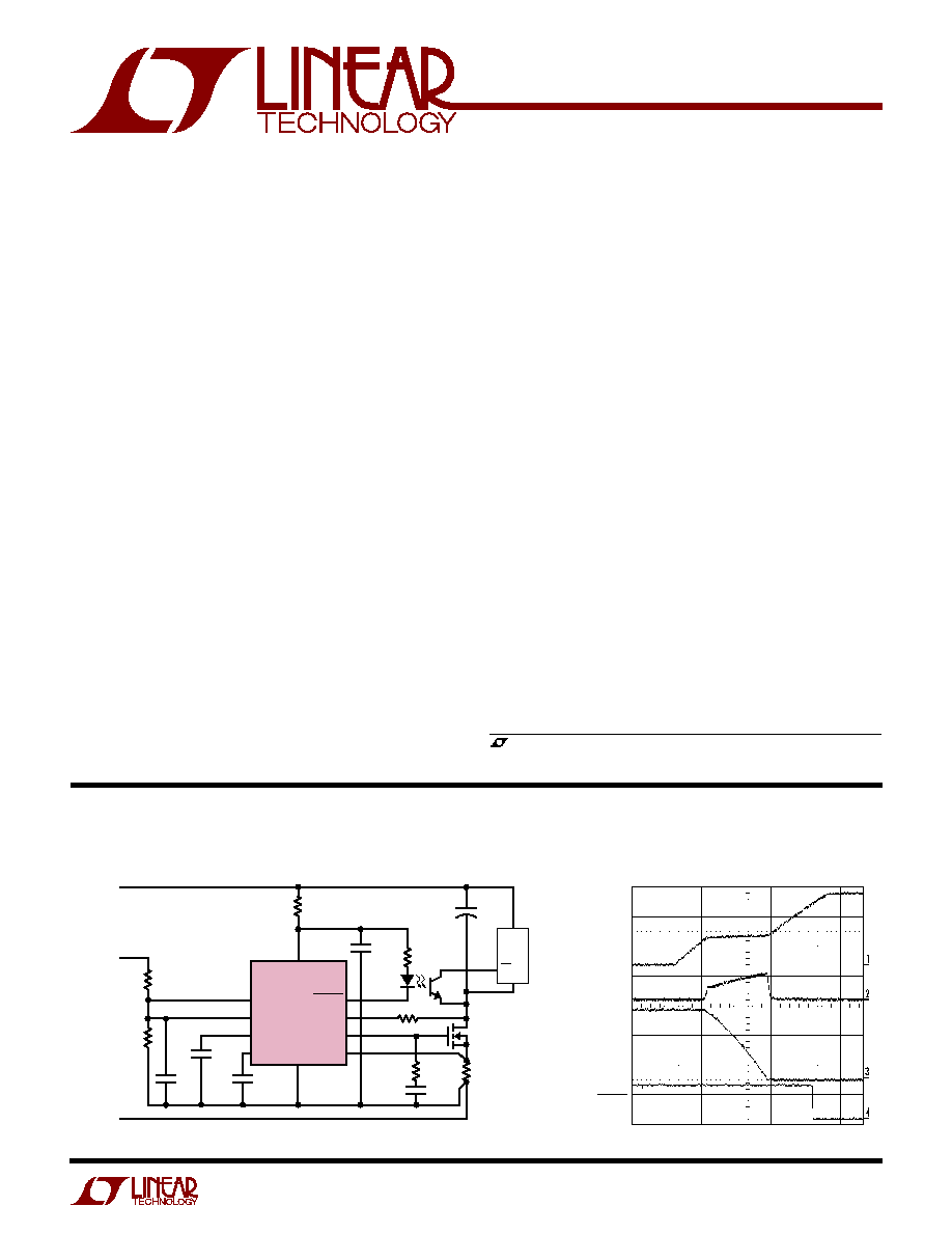
48V/2.5A Hot Swap Controller
4252-1/2 TA01
GND
OV
UV
V
EE
V
IN
SENSE
SS
TIMER
GATE
PWRGD
DRAIN
LTC4252-1
R1
402k
1%
R2
32.4k
1%
C
T
0.33
µ
F
C
SS
68nF
C
C
18nF
48V
R
S
0.02
Q1
IRF530S
V
OUT
R
C
10
R3
5.1k
R
IN
3
×
1.8k IN SERIES
1/4W EACH
1
8
9
10
3
2
7
6
4
5
C1
10nF
C
IN
1
µ
F
C
L
100
µ
F
GND
(SHORT PIN)
+
R
D
1M
LOAD
EN
*
* M0C207
4252-1/2 TA01a
GATE
5V/DIV
SENSE
2.5A/DIV
PWRGD
10V/DIV
1ms/DIV
V
OUT
20V/DIV
Start-Up Behavior
FEATURES
DESCRIPTIO
U
APPLICATIO S
U
TYPICAL APPLICATIO
U
LTC4252-1/LTC4252-2
2
425212f
SYMBOL
PARAMETER
CONDITIONS
MIN
TYP
MAX
UNITS
V
Z
V
IN
V
EE
Zener Voltage
I
IN
= 2mA
q
12
13
14.5
V
r
Z
V
IN
V
EE
Zener Dynamic Impedance
I
IN
= 2mA to 30mA
5
I
IN
V
IN
Supply Current
UV = OV = 4V, V
IN
= (V
Z
0.3V)
q
0.8
2
mA
V
LKO
V
IN
Undervoltage Lockout
Coming Out of UVLO (Rising V
IN
)
q
9.2
12
V
V
LKH
V
IN
Undervoltage Lockout Hysteresis
1
V
V
CB
Circuit Breaker Current Limit Voltage
V
CB
= (V
SENSE
V
EE
)
q
40
50
60
mV
V
ACL
Analog Current Limit Voltage
V
ACL
= (V
SENSE
V
EE
), SS = Open or 2.2V
q
80
100
120
mV
V
FCL
Fast Current Limit Voltage
V
FCL
= (V
SENSE
V
EE
)
q
150
200
300
mV
V
SS
SS Voltage
After End of SS Timing Cycle
2.2
V
R
SS
SS Output Impedance
100
k
I
SS
SS Pin Current
UV = OV = 4V, V
SENSE
= V
EE
, V
SS
= 0V (Sourcing)
22
µ
A
UV = OV = 0V, V
SENSE
= V
EE
, V
SS
= 2V (Sinking)
28
mA
V
OS
Analog Current Limit Offset Voltage
10
mV
V
ACL
+V
OS
Ratio (V
ACL
+ V
OS
) to SS Voltage
0.05
V/V
V
SS
Current into V
IN
(100
µ
s Pulse) ........................... 100mA
V
IN
, DRAIN Pin Minimum Voltage ....................... 0.3V
Input/Output Pins
(Except SENSE and DRAIN) Voltage .......... 0.3V to 16V
SENSE Pin Voltage ................................... 0.6V to 16V
Current Out of SENSE Pin (20
µ
s Pulse) ........... 200mA
Current into DRAIN Pin (100
µ
s Pulse) ................. 20mA
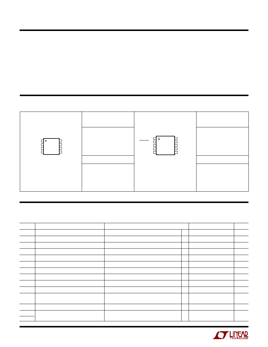
ORDER PART
NUMBER
MS PART MARKING
T
JMAX
= 125
°
C,
JA
= 160
°
C/W
Consult LTC Marketing for parts specified with wider operating temperature ranges.
LTWN
LTWQ
LTRS
LTRT
LTC4252-1CMS
LTC4252-2CMS
LTC4252-1IMS
LTC4252-2IMS
ABSOLUTE AXI U
RATI GS
W
W
W
U
PACKAGE/ORDER I FOR ATIO
U
U
W
All Voltages Referred to V
EE
(Note 1)
ELECTRICAL CHARACTERISTICS
The
q
denotes the specifications which apply over the full operating
temperature range, otherwise specifications are at T
A
= 25
°
C. (Note 2)
Maximum Junction Temperature .......................... 125
°
C
Operating Temperature Range
LTC4252-1C/LTC4252-2C ....................... 0
°
C to 70
°
C
LTC4252-1I/LTC4252-2I ................... 40
°
C to 85
°
C
Storage Temperature Range ................. 65
°
C to 150
°
C
Lead Temperature (Soldering, 10 sec).................. 300
°
C
T
JMAX
= 125
°
C,
JA
= 160
°
C/W
ORDER PART
NUMBER
MS8 PART MARKING
LTWM
LTWP
LTRQ
LTRR
LTC4252-1CMS8
LTC4252-2CMS8
LTC4252-1IMS8
LTC4252-2IMS8
1
2
3
4
5
V
IN
PWRGD
SS
SENSE
V
EE
10
9
8
7
6
TIMER
UV
OV
DRAIN
GATE
TOP VIEW
MS PACKAGE
10-LEAD PLASTIC MSOP
1
2
3
4
8
7
6
5
TOP VIEW
MS8 PACKAGE
8-LEAD PLASTIC MSOP
V
IN
SS
SENSE
V
EE
TIMER
UV/OV
DRAIN
GATE
LTC4252-1/LTC4252-2
3
425212f
ELECTRICAL CHARACTERISTICS
The
q
denotes the specifications which apply over the full operating
temperature range, otherwise specifications are at T
A
= 25
°
C. (Note 2)
SYMBOL
PARAMETER
CONDITIONS
MIN
TYP
MAX
UNITS
I
GATE
GATE Pin Output Current
UV = OV = 4V, V
SENSE
= V
EE
,
q
40
58
80
µ
A
V
GATE
= 0V (Sourcing)
UV = OV = 4V, V
SENSE
V
EE
= 0.15V,
17
mA
V
GATE
= 3V (Sinking)
UV = OV = 4V, V
SENSE
V
EE
= 0.3V,
190
mA
V
GATE
= 1V (Sinking)
V
GATE
External MOSFET Gate Drive
V
GATE
V
EE
, I
IN
= 2mA
q
10
12
V
Z
V
V
GATEH
Gate High Threshold
V
GATEH
= V
IN
V
GATE
, I
IN
= 2mA,
2.8
V
for PWRGD Status (MS Only)
V
GATEL
Gate Low Threshold
(Before Gate Ramp-Up)
0.5
V
V
UVHI
UV Pin Threshold HIGH
q
3.075
3.225
3.375
V
V
UVLO
UV Pin Threshold LOW
q
2.775
2.925
3.075
V
V
UVHST
UV Pin Hysteresis
0.3
V
V
OVHI
OV Pin Threshold HIGH
q
5.85
6.15
6.45
V
V
OVLO
OV Pin Threshold LOW
q
5.25
5.55
5.85
V
V
OVHST
OV Pin Hysteresis
0.6
V
I
SENSE
SENSE Pin Input Current
UV = OV = 4V, V
SENSE
= 50mV
q
30
15
µ
A
I
INP
UV, OV Pin Input Current
UV = OV = 4V
q
±
0.1
±
10
µ
A
V
TMRH
TIMER Pin Voltage High Threshold
4
V
V
TMRL
TIMER Pin Voltage Low Threshold
1
V
I
TMR
TIMER Pin Current
Timer On (Initial Cycle/Latchoff/
5.8
µ
A
Shutdown Cooling, Sourcing), V
TMR
= 2V
Timer Off (Initial Cycle, Sinking), V
TMR
= 2V
28
mA
Timer On (Circuit Breaker, Sourcing,
230
µ
A
I
DRN
= 0
µ
A), V
TMR
= 2V
Timer On (Circuit Breaker, Sourcing,
630
µ
A
I
DRN
= 50
µ
A), V
TMR
= 2V
Timer Off (Circuit Breaker/
5.8
µ
A
Shutdown Cooling, Sinking), V
TMR
= 2V
I
TMRACC
[(I
TMR
at I
DRN
= 50
µ
A) (I
TMR
at I
DRN
= 0
µ
A)]
Timer On (Circuit Breaker with I
DRN
= 50
µ
A)
8
µ
A/
µ
A
I
DRN
50
µ
A
V
DRNL
DRAIN Pin Voltage Low Threshold
For PWRGD Status (MS Only)
2.385
V
I
DRNL
DRAIN Leakage Current
V
DRAIN
= 5V
±
0.1
±
1
µ
A
V
DRNCL
DRAIN Pin Clamp Voltage
I
DRN
= 50
µ
A
7
V
V
PGL
PWRGD Output Low Voltage
I
PG
= 1.6mA (MS Only)
q
0.2
0.4
V
I
PG
= 5mA (MS Only)
q
1.1
V
I
PGH
PWRGD Pull-Up Current
V
PWRGD
= 0V (Sourcing) (MS Only)
q
40
58
80
µ
A
t
SS
SS Default Ramp Period
SS pin floating, V
SS
ramps from 0.2V to 2V
180
µ
s
t
PLLUG
UV Low to Gate Low
0.4
µ
s
t
PHLOG
OV High to Gate Low
0.4
µ
s
Note 1: Absolute Maximum Ratings are those values beyond which the life
of a device may be impaired.
Note 2: All currents into device pins are positive; all currents out of device
pins are negative. All voltages are referenced to V
EE
unless otherwise
specified.
LTC4252-1/LTC4252-2
4
425212f
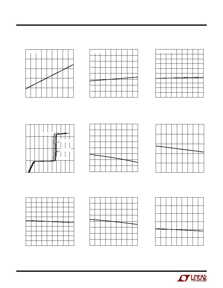
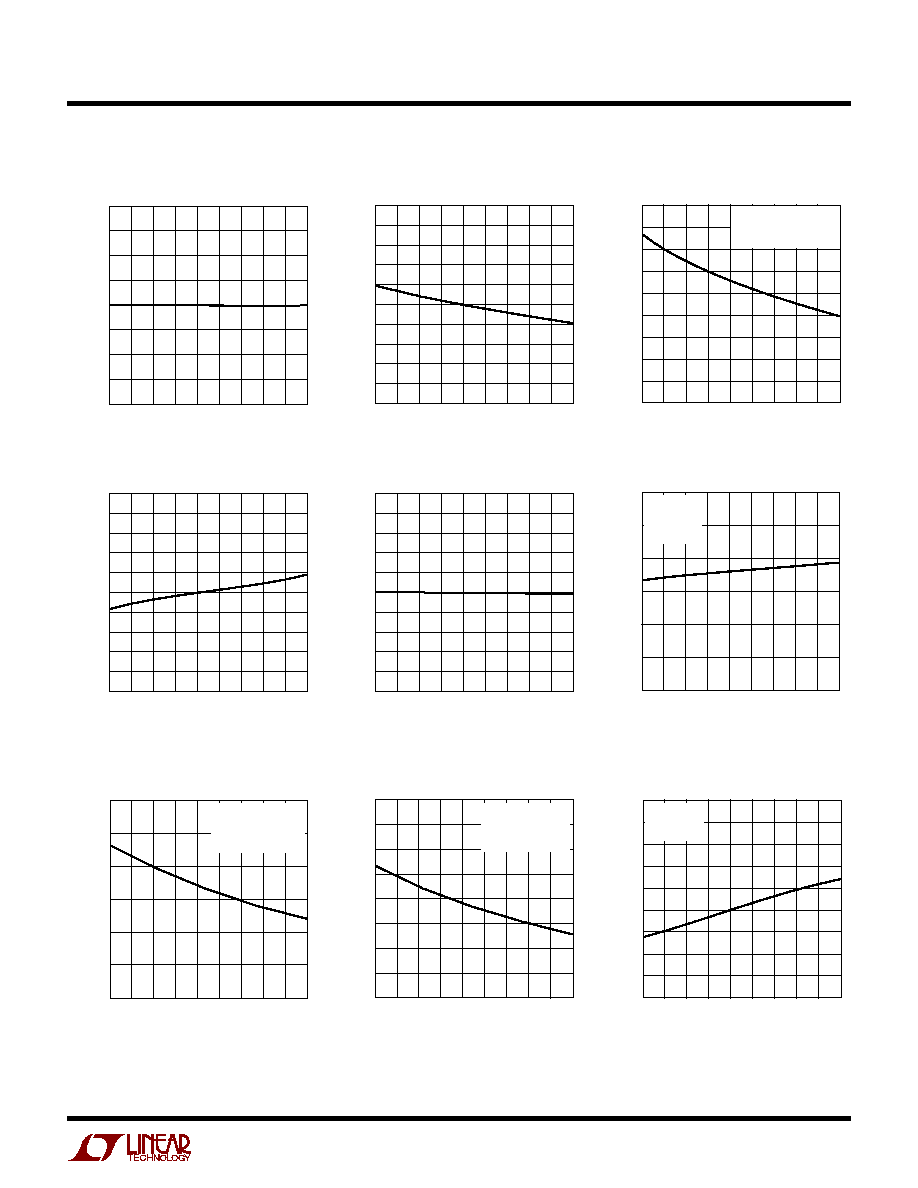
TYPICAL PERFOR A CE CHARACTERISTICS
U
W
I
IN
vs Temperature
r
Z
vs Temperature
V
Z
vs Temperature
Undervoltage Lockout V
LKO
vs Temperature
Undervoltage Lockout Hysteresis
V
LKH
vs Temperature
Circuit Breaker Current Limit
Voltage V
CB
vs Temperature
Analog Current Limit Voltage
V
ACL
vs Temperature
Fast Current Limit Voltage V
FCL
vs Temperature
TEMPERATURE (
°
C)
55
I
IN
(
µ
A)
2000
1800
1600
1400
1200
1000
800
600
400
200
0
15
25
45
125
4252-1/2 G01
35
5
65
85 105
V
IN
= (V
Z
0.3V)
V
IN
(V)
0
2
4
6
8
10 12 14 16 18 20 22
I
IN
(mA)
1000
100
10
1
0.1
4252-1/2
G02
T
A
= 40
°
C
T
A
= 125
°
C
T
A
= 85
°
C
T
A
= 25
°
C
TEMPERATURE (
°
C)
55
r
Z
(
)
10
9
8
7
6
5
4
3
2
15
25
45
125
4252-1/2 G03
35
5
65
85 105
I
IN
= 2mA
TEMPERATURE (
°
C)
55
V
Z
(V)
14.5
14.0
13.5
13.0
12.5
12.0
15
25
45
125
4252-1/2 G04
35
5
65
85 105
I
IN
= 2mA
TEMPERATURE (
°
C)
55
V
LKO
(V)
12.0
11.5
11.0
10.5
10.0
9.5
9.0
8.5
8.0
15
25
45
125
4252-1/2 G05
35
5
65
85 105
TEMPERATURE (
°
C)
55
0.5
V
LKH
(V)
0.7
1.1
1.3
1.5
15
25
45
125
4252-1/2 G06
0.9
35
5
65
95 105
TEMPERATURE (
°
C)
55
V
CB
(mV)
60
58
56
54
52
50
48
46
44
42
40
15
25
45
125
4252-1/2 G07
35
5
65
85 105
TEMPERATURE (
°
C)
55
V
ACL
(mV)
120
115
110
105
100
95
90
85
80
15
25
45
125
4252-1/2 G08
35
5
65
85 105
TEMPERATURE (
°
C)
55
V
FCL
(mV)
300
275
250
225
200
175
150
15
25
45
125
4252-1/2 G09
35
5
65
85 105
I
IN
vs V
IN
LTC4252-1/LTC4252-2
5
425212f
TYPICAL PERFOR A CE CHARACTERISTICS
U
W
I
GATE
(ACL, Sinking)
vs Temperature
I
GATE
(FCL, Sinking)
vs Temperature
V
GATE
vs Temperature
V
SS
vs Temperature
R
SS
vs Temperature
I
SS
(Sinking) vs Temperature
V
OS
vs Temperature
(V
ACL
+ V
OS
)/V
SS
vs Temperature
I
GATE
(Sourcing) vs Temperature
TEMPERATURE (
°
C)
55 35 15
5
25
45
65
85 105 125
V
SS
(V)
4252-1/2 G26
2.40
2.35
2.30
2.25
2.20
2.15
2.10
2.05
2.00
TEMPERATURE (
°
C)
55 35 15
5
25
45
65
85 105 125
R
SS
(k
)
4252-1/2 G28
110
108
106
104
102
100
98
96
94
92
90
TEMPERATURE (
°
C)
55 35 15
0
I
SS
(mA)
5
15
20
25
65
85 105
45
4252-1/2 G39
10
5
25
45
125
30
35
40
UV = OV = V
SENSE
= V
EE
I
IN
= 2mA
V
SS
= 2V
TEMPERATURE (
°
C)
55 35 15
5
25
45
65
85 105 125
V
OS
(mV)
4252-1/2 G29
11.0
10.8
10.6
10.4
10.2
10.0
9.8
9.6
9.4
9.2
9.0
TEMPERATURE (
°
C)
55 35 15
5
25
45
65
85 105 125
(V
ACL
+ V
OS
)/V
SS
(V/V)
4252-1/2 G30
0.060
0.058
0.056
0.054
0.052
0.050
0.048
0.046
0.044
0.042
0.040
TEMPERATURE (
°
C)
55
I
GATE
(
µ
A)
70
65
60
55
50
45
40
15
25
45
125
4252-1/2 G10
35
5
65
85 105
UV/0V = 4V
TIMER = 0V
V
SENSE
= V
EE
V
GATE
= 0V
TEMPERATURE (
°
C)
55
I
GATE
(mA)
30
25
20
15
10
5
0
15
25
45
125
4252-1/2 G11
35
5
65
85 105
UV/0V = 4V
TIMER = 0V
V
SENSE
V
EE
= 0.15V
V
GATE
= 3V
TEMPERATURE (
°
C)
55
I
GATE
(mA)
400
350
300
250
200
150
100
50
0
15
25
45
125
4252-1/2 G12
35
5
65
85 105
UV/0V = 4V
TIMER = 0V
V
SENSE
V
EE
= 0.3V
V
GATE
= 1V
TEMPERATURE (
°
C)
55
V
GATE
(V)
14.5
14.0
13.5
13.0
12.5
12.0
11.5
11.0
10.5
10.0
15
25
45
125
4252-1/2 G13
35
5
65
85 105
UV/0V = 4V
TIMER = 0V
V
SENSE
= V
EE