 | ÐлекÑÑоннÑй компоненÑ: LTC4259A | СкаÑаÑÑ:  PDF PDF  ZIP ZIP |
Äîêóìåíòàöèÿ è îïèñàíèÿ www.docs.chipfind.ru
LTC4259A
1
4259Af
, LTC and LT are registered trademarks of Linear Technology Corporation.
s
Controls Four Independent 48V Powered
Ethernet Ports
s
Each Port Includes:
IEEE 802
®
.3af Compliant PD Detection and
Classification
Output Current Limit with Foldback
Short-Circuit Protection with Fast Gate Pull-Down
PD Disconnect Using AC or DC Sensing
Power Good Indication
s
Operates Autonomously or Controlled by I
2
C
TM
Serial Interface
s
4-Bit Programmable Digital Address Allows Control
of Up to 64 Ports
s
Programmable INT Pin Eliminates Software Polling
s
Current and Duty Cycle Limits Protect External FETs
s
Available in a 36-Pin SSOP Package
Quad IEEE 802.3af
Power over Ethernet Controller
with AC Disconnect
s
IEEE 802.3af Compliant Endpoint and Midspan
Power Sources
s
IP Phone Systems
s
DTE Power Distribution
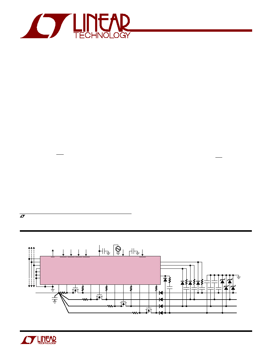
The LTC
®
4259A is a quad 48V Hot Swap
TM
controller
designed for use in IEEE 802.3af compliant Power
Sourcing Equipment (PSE). It consists of four independent
ports, each with output current limit, short-circuit protec-
tion, complete Powered Device (PD) detection and classi-
fication capability, and programmable PD disconnect using
AC or DC sensing. Used with power MOSFETs and passives
as in Figure 1, the LTC4259A can implement a complete IEEE
802.3af-compliant PSE.
The LTC4259A can operate autonomously or be controlled
by an I
2
C serial interface. Up to 16 LTC4259As may coexist
on the same data bus, allowing up to 64 powered Ethernet
ports to be controlled with only two digital lines. Fault con-
ditions are optionally signaled with the INT pin to eliminate
software polling.
External power MOSFETs, current sense resistors and di-
odes allow easy scaling of current and power dissipation
levels and provide protection against voltage and current
spikes and ESD events.
The LTC4259A is available in a 36-pin SSOP package.
Linear Technology also provides solutions for 802.3af PD
applications with the LTC4257 and LTC4257-1.
Hot Swap is a trademark of Linear Technology Corporation. 802 is a registered trademark of
Instutute of Electrical and Electronics Engineers, Inc. I
2
C is a trademark of Philips Electronics N.V.
Figure 1. Complete 4-Port Powered Ethernet Power Source
DGND
AD3
RS1 TO RS4: 0.5
Q1 TO Q4: IRFM120A
AD2
AD1
AD0
SDAOUT
SDAIN
SCL
DETECT4
DETECT3
DETECT1
DETECT2
AGND
INT
48V
V
EE
SHDN1
SENSE1
R
S1
R
S2
R
S3
R
S4
GATE1
Q1
Q2
Q3
Q4
S1B
×
4
CMPD3003
×
4
10k
10k
10k
10k
1k
×
4
0.47
µ
F
100V
×
4
X7R
PORT1
PORT2
PORT3
PORT4
4259A F01
SMAJ58A
×
4
0.1
µ
F 100V
×
4
OUT1 SENSE2 GATE2
LTC4259A
OUT2 SENSE3 GATE3 OUT3 SENSE4 GATE4 OUT4
SHDN2 SHDN3 SHDN4
V
DD
3.3V
0.1
µ
F
AUTO BYP
OSCIN
RESET
0.1
µ
F
100V X7R
0.1
µ
F
FEATURES
DESCRIPTIO
U
APPLICATIO S
U
TYPICAL APPLICATIO
U
LTC4259A
2
4259Af
Supply Voltages
V
DD
to DGND .......................................... 0.3V to 5V
V
EE
to AGND ......................................... 0.3V to 70V
DGND to AGND (Note 2) ....................................
±
1V
Digital Pins
SCL, SDAIN, SDAOUT, INT, AUTO, RESET
SHDN
n, ADn ................. DGND 0.3V to DGND + 5V
Analog Pins
GATE
n (Note 3) ................... V
EE
0.3V to V
EE
+ 12V
DETECT
n Peak Currents (Note 4) ..................
±
80mA
SENSE
n ................................. V
EE
0.3V to V
EE
+ 1V
OUT
n .................................... V
EE
70V to V
EE
+ 70V
OSCIN .......................... DGND 0.3V to DGND + 5V
BYP Current ....................................................
±
1mA
Operating Ambient Temperature Range ...... 0
°
C to 70
°
C
Junction Temperature (Note 5) ............................ 150
°
C
Storage Temperature Range ................ 65
°
C to 150
°
C
Lead Temperature (Soldering, 10 sec)................. 300
°
C
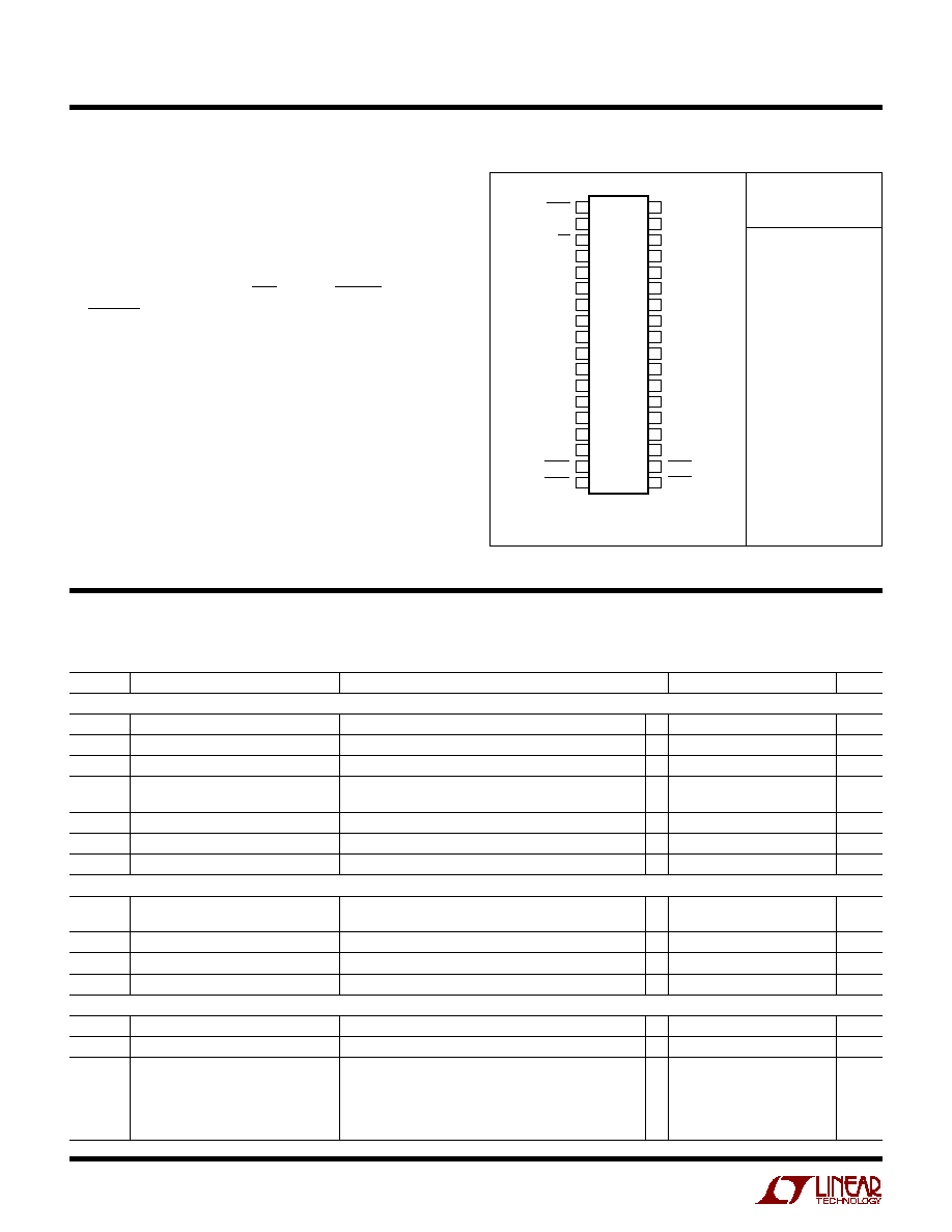
ORDER PART
NUMBER
T
JMAX
= 150
°
C,
JA
= 80
°
C/W
LTC4259ACGW
(Note 1)
ABSOLUTE AXI U RATI GS
W
W
W
U
PACKAGE/ORDER I FOR ATIO
U
U
W
Consult LTC Marketing for parts specified with wider operating temperature ranges.
1
2
3
4
5
6
7
8
9
10
11
12
13
14
15
16
17
18
TOP VIEW
GW PACKAGE
36-LEAD PLASTIC SSOP
36
35
34
33
32
31
30
29
28
27
26
25
24
23
22
21
20
19
RESET
BYP
INT
SCL
SDAOUT
SDAIN
AD3
AD2
AD1
AD0
DETECT1
DETECT2
DETECT3
DETECT4
DGND
V
DD
SHDN1
SHDN2
OSCIN
AUTO
OUT1
GATE1
SENSE1
OUT2
GATE2
SENSE2
V
EE
OUT3
GATE3
SENSE3
OUT4
GATE4
SENSE4
AGND
SHDN4
SHDN3
ELECTRICAL CHARACTERISTICS
The
q
denotes the specifications which apply over the full operating
temperature range, otherwise specifications are at T
A
= 25
°
C. AGND = DGND = 0V, V
DD
= 3.3V, V
EE
= 48V unless otherwise noted
(Note 6).
SYMBOL
PARAMETER
CONDITIONS
MIN
TYP
MAX
UNITS
Power Supplies
V
DD
V
DD
Supply Voltage
q
3
3.3
4
V
V
EE
V
EE
Supply Voltage
To Maintain IEEE Compliant Output (Note 7)
q
48
57
V
I
DD
V
DD
Supply Current
q
2.5
5
mA
I
EE
V
EE
Supply Current
Normal Operation
q
2
5
mA
Classification Into a Short (V
DETECT
n
= 0V) (Note 8)
q
100
mA
V
DDMIN
V
DD
UVLO Voltage
2.7
V
V
EEMINON
V
EE
UVLO Voltage (Turning On)
V
EE
AGND
31
V
V
EEMINOFF
V
EE
UVLO Voltage (Turning Off)
V
EE
AGND
28
V
Detection
I
DET
Detection Current
First Point, V
DETECT
n
= 10V
q
235
300
µ
A
Second Point, V
DETECT
n
= 3.5V
q
145
190
µ
A
V
DET
Detection Voltage Compliance
Open Circuit, Measured at DETECT
n Pin
q
20
23
V
R
DETMIN
Minimum Valid Signature Resistance
q
15.2
17
19
k
R
DETMAX
Maximum Valid Signature Resistance
q
26.7
29
33
k
Classification
V
CLASS
Classification Voltage
0mA < I
CLASS
< 31mA
q
16.4
21
V
I
CLASS
Classification Current Compliance
Into Short (V
DETECT
= 0V)
q
55
75
mA
I
TCLASS
Classification Threshold Current
Class 0-1
q
5.5
6.5
7.5
mA
Class 1-2
q
13
14.5
16
mA
Class 2-3
q
21
23
25
mA
Class 3-4
q
31
33
35
mA
Class 4-Overcurrent
q
45
48
51
mA

LTC4259A
3
4259Af
ELECTRICAL CHARACTERISTICS
The
q
denotes the specifications which apply over the full operating
temperature range, otherwise specifications are at T
A
= 25
°
C. AGND = DGND = 0V, V
DD
= 3.3V, V
EE
= 48V unless otherwise noted
(Note 6).
SYMBOL
PARAMETER
CONDITIONS
MIN
TYP
MAX
UNITS
Gate Driver
I
GON
GATE Pin Current
Gate On, V
GATE
n
= V
EE
q
20
50
70
µ
A
I
GOFF
GATE Pin Current
Gate Off, V
GATE
n
= V
EE
+ 5V
q
30
50
95
µ
A
I
GPD
GATE Pin Short-Circuit Pull-Down
V
GATE
n
= V
EE
+ 5V
100
mA
V
GATE
External Gate Voltage (V
GATE
n
V
EE
)
I
GATE
= 1
µ
A (Note 3)
q
10
13
15
V
Output Voltage Sense
V
PG
Power Good Threshold Voltage
V
OUT
n
V
EE
q
1
2
3
V
I
VOUT
Out Pin Bias Current
0V > V
OUT
> 10V
q
6
µ
A
10V > V
OUT
> 30V
q
18
µ
A
V
OUT
= 48V
20
µ
A
Current Sense
V
CUT
Overcurrent Detection Sense Voltage
V
SENSE
n
V
EE
, V
OUT
= V
EE
(Note 9)
166
187.5
199
mV
V
LIM
Current Limit Sense Voltage
V
SENSE
n
V
EE
, V
OUT
= V
EE
201
212.5
224
mV
V
SENSE
n
V
EE
, V
OUT
= AGND 30V
201
224
mV
V
SENSE
n
V
EE
, V
OUT
= AGND 10V
30.2
mV
V
MIN
DC Disconnect Sense Voltage
V
SENSE
n
V
EE
2.52
3.75
4.97
mV
V
SC
Short-Circuit Sense Voltage
275
mV
I
SENSE
SENSE Pin Bias Current
V
SENSE
n
= V
EE
50
µ
A
AC Disconnect (Note 10)
R
OSCIN
Input Impedance of OSCIN Pin
0.1V < V
OSCIN
< 3V, f
SINEIN
< 200Hz
q
200
500
k
A
VACD
Voltage Gain OSCIN to DETECT1, 2
Port Powered, PD Not Present
q
2.7
3
3.3
V/V
Voltage Gain OSCIN to DETECT3, 4
Port Powered, PD Not Present
q
2.7
3
3.3
V/V
I
ACDMAX
AC Disconnect DETECT
n Output Current
Port Powered, 6V < V
DETECT
n
< 0V
q
±
600
µ
A
I
ACDMIN
Remain Connected DETECT Pin Current
Port Powered, V
DETECT
n
= 3.4V
q
150
200
260
µ
A
Digital Interface
V
OLD
Digital Output Low Voltage
I
SDAOUT
= 3mA, I
INT
= 3mA
q
0.4
V
I
SDAOUT
= 5mA, I
INT
= 5mA
q
0.7
V
V
ILD
Digital Input Low Voltage
SCL, SDAIN, RESET, SHDN
n, AUTO
q
0.8
V
V
IHD
Digital Input High Voltage
SCL, SDAIN, RESET, SHDN
n, AUTO
q
2.4
V
R
PU
Pull-Up Resistor to V
DD
AD0 to AD3, RESET, SHDN
n
50
k
R
PD
Pull-Down Resistor to DGND
AUTO
50
k
AC Characteristics
t
DETDLY
Detection Delay
From Detect Command or Application of PD to Port
q
170
590
ms
to Detect Complete
t
DET
Detection Duration
Time to Measure PD Signature Resistance (Figure 2)
q
170
230
ms
t
CLSDLY
Classification Delay
From Successful Detect in Auto or Semiauto Mode
q
10.1
52
ms
to Class Complete
From Classify Command in Manual
q
10.1
420
ms
t
CLASS
Classification Duration
(Figure 2)
q
10.1
13
ms
t
PON
Power On Delay, Auto Mode
From Valid Detect to Port On in Auto Mode (Figure 2)
q
90
ms
From Port On Command to GATE Pin Current = I
GON
q
1
ms
(Note 10)
t
START
Maximum Current Limit Duration During
t
START1
= 0, t
START0
= 0 (Figure 3)
q
50
60
70
ms
Port Start-Up
t
START1
= 0, t
START0
= 1
q
25
30
35
ms
t
START1
= 1, t
START0
= 0
q
100
120
140
ms
t
START1
= 1, t
START0
= 1
q
200
240
280
ms
LTC4259A
4
4259Af
Note 7: The LTC4259A is designed to maintain a port voltage of 46.6V to
57V and the V
EE
supply voltage range accounts for the drop across the
diode, MOSFET and sense resistor.
Note 8: V
EE
supply current, while classifying a short, is measured
indirectly by measuring the DETECT
n pin current while classifying a short.
Note 9: The LTC4259A implements overload current detection per IEEE
802.3af. The minimum overload current (I
CUT
) is dependent on port
voltage; I
CUT_MIN
= 15.4W/V
PORT_MIN
. An IEEE compliant system using the
LTC4259A should maintain port voltage above 46.6V.
Note 10: Unless otherwise specified, AC disconnect specifications require
the following conditions: the DETECT pin is connected to the port as
shown in Figure 1, a valid sine wave is applied to OSCIN, the OSCFAIL bit
is cleared and the AC Disconnect Enable bits are set.
Note 11: Guaranteed by design, not subject to test.
Note 12: Values measured at V
ILD
and V
IHD
.
Note 13: If fault occurs during an I
2
C transaction, the INT pin will not be
pulled down until a stop condition is present on the I
2
C bus.
Note 1: Absolute Maximum Ratings are those values beyond which the life
of the device may be impaired.
Note 2: DGND and AGND should be tied together in normal operation.
Note 3: An internal clamp limits the GATE pins to a minimum of 12V above
V
EE
. Driving this pin beyond the clamp may damage the part.
Note 4: When a port powers on or off, the transient voltage on the port
couples through C
DET
(Figure 16). The LTC4259A contains internal
protection circuitry to withstand transient currents of up to 80mA for 5ms.
As long as the absolute value of the current remains below 80mA, the
LTC4259A will keep the voltage at the DETECT
n pin within the absolute
maximum voltage range. A properly sized R
DET
should limit the current to
less than 60mA.
Note 5: This IC includes overtemperature protection that is intended to
protect the device during momentary overload conditions. Junction
temperature will exceed 125
°
C when overtemperature protection is active.
Continuous operation above the specified maximum operating junction
temperature may impair device reliability.
Note 6: All currents into device pins are positive; all currents out of device
pins are negative. All voltages are referenced to ground (AGND and DGND)
unless otherwise specified.
ELECTRICAL CHARACTERISTICS
The
q
denotes the specifications which apply over the full operating
temperature range, otherwise specifications are at T
A
= 25
°
C. AGND = DGND = 0V, V
DD
= 3.3V, V
EE
= 48V unless otherwise noted
(Note 6).
SYMBOL
PARAMETER
CONDITIONS
MIN
TYP
MAX
UNITS
t
ICUT
Maximum Current Limit Duration After
t
ICUT1
= 0, t
ICUT0
= 0 (Figure 3)
q
50
60
70
ms
Port Start-Up
t
ICUT1
= 0, t
ICUT0
= 1
q
25
30
35
ms
t
ICUT1
= 1, t
ICUT0
= 0
q
100
120
140
ms
t
ICUT1
= 1, t
ICUT0
= 1
q
200
240
280
ms
DC
CLMAX
Maximum Current Limit Duty Cycle
Reg16h = 00h
q
5.8
6.3
6.7
%
t
DIS
Disconnect Delay
t
DIS1
= 0, t
DIS0
= 0 (Figures 4, 5)
q
300
360
400
ms
t
DIS1
= 0, t
DIS0
= 1
q
75
90
100
ms
t
DIS1
= 1, t
DIS0
= 0
q
150
180
200
ms
t
DIS1
= 1, t
DIS0
= 1
q
600
720
800
ms
t
VMIN
DC Disconnect Minimum Pulse
V
SENSE
n
V
EE
> 5mV, V
OUT
n
= 48V (Figure 4)
q
0.02
1
ms
Width Sensitivity
(Note 11)
I
2
C Timing
f
SCLK
Clock Frequency
(Note 11)
q
400
kHz
t
1
Bus Free Time
Figure 6 (Notes 11, 12)
q
1.3
µ
s
t
2
Start Hold Time
Figure 6 (Notes 11, 12)
q
600
ns
t
3
SCL Low Time
Figure 6 (Notes 11, 12)
q
1.3
µ
s
t
4
SCL High Time
Figure 6 (Notes 11, 12)
q
600
ns
t
5
Data Hold Time
Figure 6 (Notes 11, 12)
q
150
ns
t
6
Data Set-Up Time
Figure 6 (Notes 11, 12)
q
200
ns
t
7
Start Set-Up Time
Figure 6 (Notes 11, 12)
q
600
ns
t
8
Stop Set-Up Time
Figure 6 (Notes 11, 12)
q
600
ns
t
r
SCL, SDAIN Rise Time
Figure 6 (Notes 11, 12)
q
20
300
ns
t
f
SCL, SDAIN Fall Time
Figure 6 (Notes 11, 12)
q
20
150
ns
t
FLTINT
Fault Present to INT Pin Low
(Notes 11, 12, 13)
q
20
150
ns
t
STOPINT
Stop Condition to INT Pin Low
(Notes 11, 12, 13)
q
60
200
ns
t
ARAINT
ARA to INT Pin High Time
(Notes 11, 12)
q
20
300
ns
LTC4259A
5
4259Af
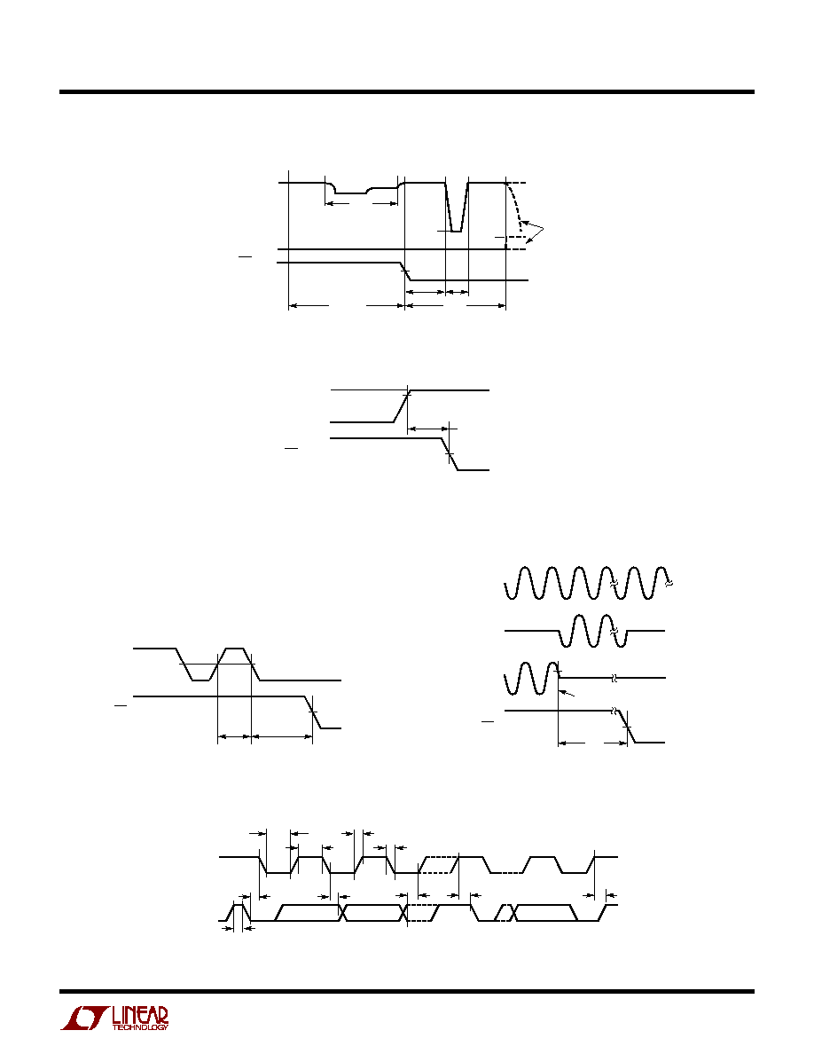
Figure 3. Current Limit Timing
Figure 4. DC Disconnect Timing
Figure 5. AC Disconnect Timing
TEST TI I G
W
U
Figure 6. I
2
C Interface Timing
Figure 2. Detect, Class and Turn-On Timing in Auto or Semiauto Modes
SCL
SDA
t
1
t
2
t
3
t
r
t
f
t
5
t
6
t
7
t
8
t
4
4259A F06
0V
V
PORT
n
V
GATE
n
INT
PD
INSERTED
V
EE
V
CLASS
V
T
PORT
TURN ON
(AUTO MODE)
t
CLSDLY
t
CLASS
4259A F02
t
DETDLY
t
DET
t
PON
V
LIM
V
CUT
0V
V
SENSE
n
TO V
EE
INT
4259A F03
t
START
, t
ICUT
V
MIN
V
SENSE
n
TO V
EE
INT
t
DIS
t
VMIN
4259A F04
INT
I
DETECT
n
V
OUT
n
V
OSCIN
t
DIS
I
ACDMIN
PD REMOVED
4259A F05