 | ÐлекÑÑоннÑй компоненÑ: LTC4401-1 | СкаÑаÑÑ:  PDF PDF  ZIP ZIP |
4401f.pm6
1
LTC4401-1/LTC4401-2
sn4401 4401fs
APPLICATIO S
U
FEATURES
DESCRIPTIO
U
TYPICAL APPLICATIO
U
RF Power Controllers
with 250kHz Loop BW
and 45dB Dynamic Range
The LTC
®
4401-1 is a SOT-23 RF power controller for slow
turn-on RF power amplifiers operating in the 800MHz to
2.7GHz range. The loop bandwidth is set at 250kHz
to improve frequency stability when controlling slow
turn-on RF power amplifiers such as the Conexant
CX77301/CX77302, CX77304, CX77314, Anadigics
AWT6107 and the RF Micro Devices RF3160.
RF power is controlled by driving the RF amplifier power
control pins and sensing the resultant RF output power
via a directional coupler. The RF sense voltage is peak
detected using an on-chip Schottky diode. This detected
voltage is compared to the DAC voltage at the PCTL pin
to control the output power. The RF power amplifier is
protected against high power control pin voltages.
Internal and external offsets are cancelled over tempera-
ture by an autozero control loop, allowing accurate low
power programming. The shutdown feature disables the
part and reduces the supply current to < 10
µ
A.
A dual control channel version (LTC4401-2) is also
available in an 8-pin MSOP package.
s
RF Power Amplifier Control in ThinSOT
TM
Package
s
Internal Schottky Diode Detector with > 45dB Range
s
Wide Input Frequency Range:
800MHz to 2.7GHz (LTC4401-1)
800MHz to 2GHz (LTC4401-2)
s
Autozero Loop Cancels Offset Errors and
Temperature Dependent Offsets
s
Wide V
CC
Range: 2.7V to 6V
s
Automatic Bandwidth Control Improves Low Power
Ramp Response
s
Allows Direct Connection to Battery
s
RF Output Power Set by External DAC
s
Internal Frequency Compensation
s
Rail-to-Rail Power Control Output
s
Power Control Signal Overvoltage Protection
s
Low Operating Current: 1mA
s
Low Shutdown Current: 10
µ
A
s
Two Pole PCTL Input Filtering
s
Low Profile (1mm) ThinSOT (LTC4401-1) and
8-Pin MSOP (LTC4401-2) Packages
, LTC and LT are registered trademarks of Linear Technology Corporation.
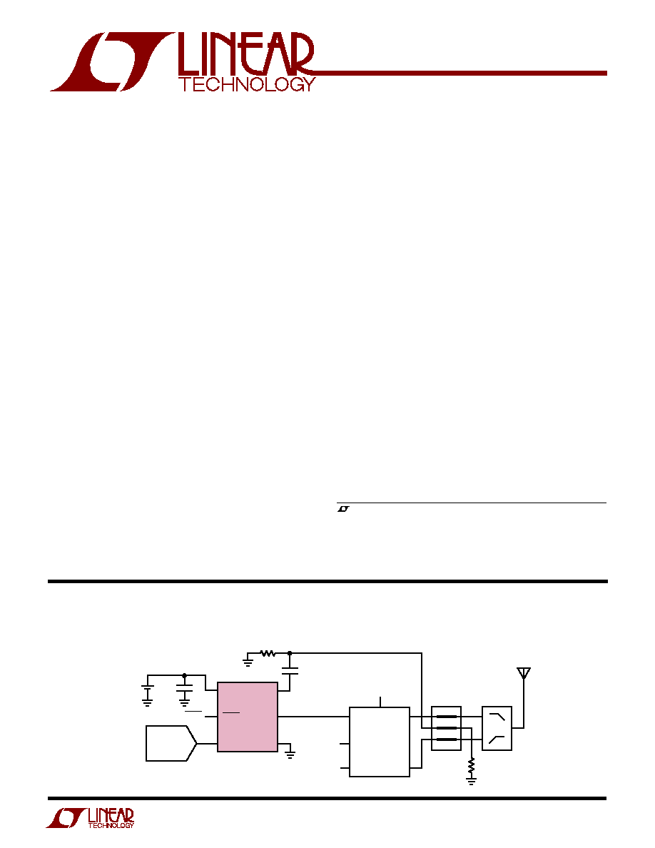
LTC4401-1 Dual Band Cellular Telephone Transmitter
s
GSM/GPRS Cellular Telephones
s
PCS Devices
s
Wireless Data Modems
s
U.S. TDMA Cellular Phones
V
CC
SHDN
PCTL
1
5
2
6
4
3
RF
V
PCA
GND
LTC4401-1
33pF
68
SHDN
DAC
1.8GHz
INPUT
900MHz
INPUT
50
4401 TA01
0.1
µ
F
Li-Ion
V
PC
900MHz
OUTPUT
1.8GHz
OUTPUT
PA MODULE
BAND
SELECT
ThinSOT is a trademark of Linear Technology Corporation.
2
LTC4401-1/LTC4401-2
sn4401 4401fs
V
CC
to GND .............................................. 0.3V to 6.5V
V
PCA/B
Voltage to GND ............................ 0.3V to 3.2V
PCTL Voltage to GND ................. 0.3V to (V
CC
+ 0.3V)
RF Voltage to GND ............................ (V
CC
2.6V) to 7V
BSEL, SHDN Voltage to GND ...... 0.3V to (V
CC
+ 0.3V)
The
q
denotes specifications which apply over the full operating
temperature range, otherwise specifications are at T
A
= 25
°
C. V
CC
= 3.6V, SHDN = HI, unless otherwise noted.
PARAMETER
CONDITIONS
MIN
TYP
MAX
UNITS
V
CC
Operating Voltage
q
2.7
6
V
I
VCC
Shutdown Current
SHDN = 0V
q
10
20
µ
A
I
VCC
Operating Current
SHDN = HI, I
VPCA/B
= 0mA
q
1.2
1.9
mA
V
PCA/B
V
OL
R
LOAD
= 400
, Enabled
q
0
0.05
V
V
PCA/B
Dropout Voltage
I
LOAD
= 6mA, V
CC
= 3V
q
V
CC
0.25
V
V
PCA/B
Voltage Clamp
PCTL = 1V
q
2.7
2.9
3.1
V
V
PCA/B
Output Current
V
PCA/B
= 2.4V, V
CC
= 3V
q
7
10
mA
V
PCA/B
Enable Time
SHDN = V
CC
(Note 5)
q
9
10.2
µ
s
V
PCA/B
Bandwidth
C
LOAD
= 100pF, R
LOAD
= 2k (Note 8)
PCTL < 80mV
q
175
250
330
kHz
PCTL > 160mV
130
kHz
V
PCA/B
Load Capacitance
(Note 6)
q
100
pF
V
PCA/B
Slew Rate
V
PCTL
= 2V Step, C
LOAD
= 100pF,
q
1
1.5
2
V/
µ
s
R
LOAD
= 400
(Note 3)
V
PCA/B
Droop
1
µ
V/ms
V
PCA/B
Start Voltage
Open Loop (Note 9)
q
300
450
550
mV
BSEL, SHDN Input Threshold
V
CC
= 2.7V to 6V
q
0.35
1.4
V
BSEL, SHDN Input Current
BSEL = SHDN = 3.6V
q
16
24
36
µ
A
PCTL Input Voltage Range
(Note 7)
q
0
2.4
V
PCTL Input Resistance
q
60
90
120
k
PCTL Input Filter
270
kHz
Autozero Range
(Note 4)
q
400
mV
ABSOLUTE AXI U RATI GS
W
W
W
U
ELECTRICAL CHARACTERISTICS
ORDER PART
NUMBER
S6 PART MARKING
LTC4401-1ES6
LTXA
T
JMAX
= 125
°
C,
JA
= 230
°
C/W
PACKAGE/ORDER I FOR ATIO
U
U
W
RF 1
GND 2
PCTL 3
6 V
CC
5 VPCA
4 SHDN
TOP VIEW
S6 PACKAGE
6-LEAD PLASTIC SOT-23
Consult LTC Marketing for parts specified with wider operating temperature ranges.
I
VPCA/B
.................................................................. 10mA
Operating Temperature Range (Note 2) .. 30
°
C to 85
°
C
Storage Temperature Range ................ 65
°
C to 150
°
C
Maximum Junction Temperature ......................... 125
°
C
Lead Temperature (Soldering, 10 sec)................. 300
°
C
(Note 1)
ORDER PART
NUMBER
MS8 PART MARKING
LTC4401-2EMS8
LTXC
T
JMAX
= 125
°
C,
JA
= 250
°
C/W
1
2
3
4
V
CC
V
PCA
V
PCB
GND
8
7
6
5
RF
BSEL
SHDN
PCTL
TOP VIEW
MS8 PACKAGE
8-LEAD PLASTIC MSOP
3
LTC4401-1/LTC4401-2
sn4401 4401fs
PARAMETER
CONDITIONS
MIN
TYP
MAX
UNITS
RF Input Frequency Range
LTC4401-1 (Note 6)
800
2700
MHz
LTC4401-2 (Note 6)
800
2000
MHz
RF Input Power Range
RF Frequency = 900MHz (Note 6)
28
18
dBm
(LTC4401-1)
RF Frequency = 1800MHz (Note 6)
26
18
dBm
RF Frequency = 2400MHz (Note 6)
24
16
dBm
RF Frequency = 2700MHz (Note 6)
22
16
dBm
RF Input Power Range
RF Frequency = 900MHz (Note 6)
28
18
dBm
(LTC4401-2)
RF Frequency = 2000MHz (Note 6)
26
18
dBm
RF Input Resistance
Referenced to V
CC
q
150
250
350
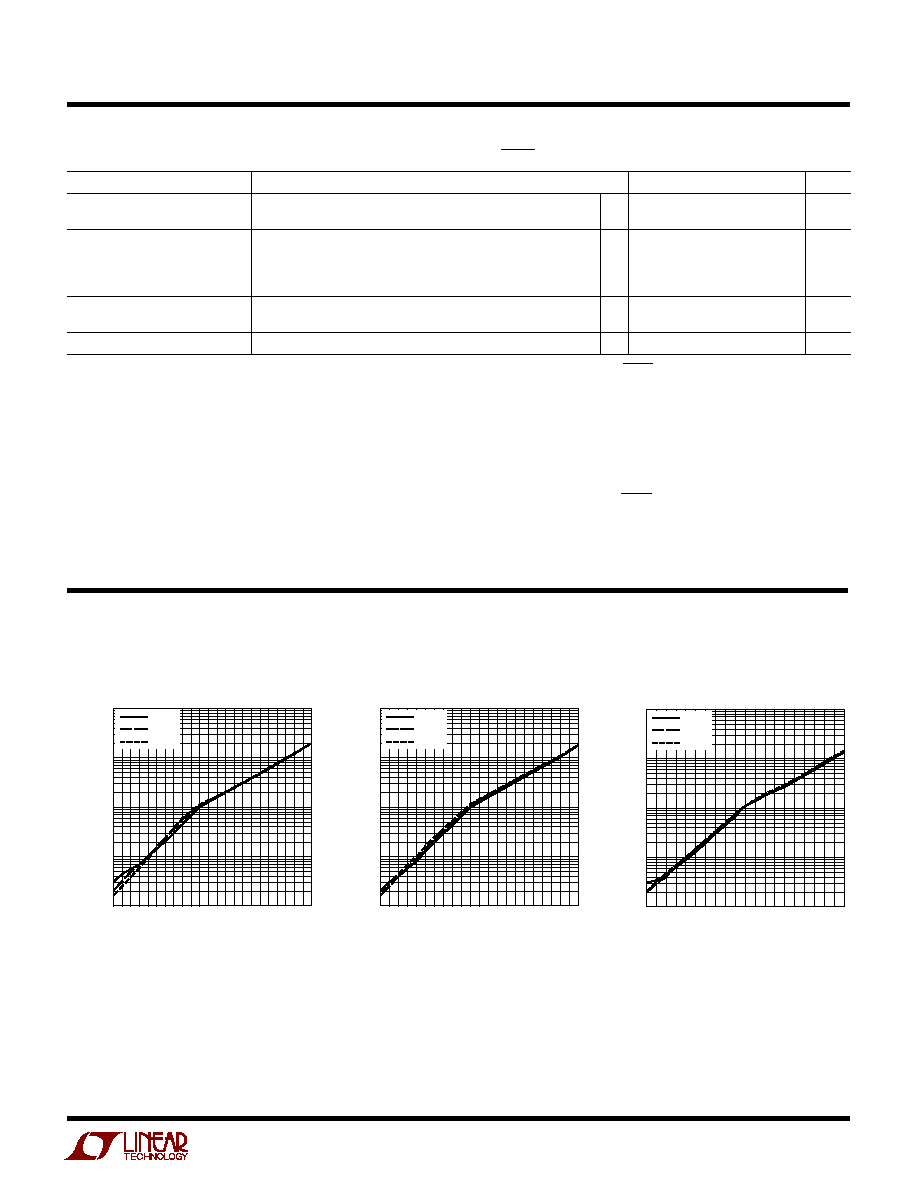
TYPICAL PERFOR A CE CHARACTERISTICS
U
W
LTC4401-1 Detector Characteristics
at 900MHz
LTC4401-1 Detector Characteristics
at 1800MHz
Note 1: Absolute Maximum Ratings are those values beyond which the life
of a device may be impaired.
Note 2: The LTC4401-X is guaranteed to meet performance specifications
from 0
°
C to 70
°
C. Specifications over the 30
°
C to 85
°
C operating
temperature range are assured by design, characterization and correlation
with statistical process controls.
Note 3: Slew rate is measured open loop. The slew time at V
PCA/B
is
measured between 1V and 2V.
Note 4: Maximum DAC zero-scale offset voltage that can be applied to
PCTL.
Note 5: This is the time from SHDN rising edge 50% switch point to
V
PCA
= 0.25V.
Note 6: Guaranteed by design. This parameter is not production tested.
Note 7: Includes maximum DAC offset voltage and maximum control
voltage.
Note 8: Bandwidth is calculated using the 10% to 90% rise time:
BW = 0.35/rise time
Note 9: Measured 12
µ
s after SHDN = HI.
RF INPUT POWER (dBm)
10
PCTL REFERENCED DETECTOR OUTPUT VOLTAGE (mV)
100
1000
10000
28
10
2
8
1
22
4
14
16
4401 G01
75
°
C
25
°
C
30
°
C
RF INPUT POWER (dBm)
10
PCTL REFERENCED DETECTOR OUTPUT VOLTAGE (mV)
100
1000
10000
26
14
8
2
4
10
16
1
20
4401 G02
75
°
C
25
°
C
30
°
C
ELECTRICAL CHARACTERISTICS
The
q
denotes specifications which apply over the full operating
temperature range, otherwise specifications are at T
A
= 25
°
C. V
CC
= 3.6V, SHDN = HI, unless otherwise noted.
LTC4401-1 Detector Characteristics
at 2400MHz
RF INPUT POWER (dBm)
10
PCTL REFERENCED DETECTOR OUTPUT VOLTAGE (mV)
100
1000
10000
24
12 8 4
4
0
8
12 16
1
20 16
4401 G03
75
°
C
25
°
C
30
°
C
4
LTC4401-1/LTC4401-2
sn4401 4401fs
RF (Pins 1/8): RF Feedback Voltage from the Directional
Coupler. Referenced to V
CC
. A coupling capacitor of 33pF
must be used to connect to the ground referenced direc-
tional coupler. The frequency range is 800MHz to 2700MHz
for the LTC4401-1 and 800MHz to 2000MHz for the
LTC4401-2. This pin has an internal 250
termination, an
internal Schottky diode detector and peak detector capaci-
tor.
GND (Pins 2/4): System Ground.
PCTL (Pins 3/5): Analog Input. The external power control
DAC drives this input. The amplifier servos the RF power
until the RF detected signal equals the DAC signal. The
input impedance is typically 90k
.
V
PCB
(Pin 3): (LTC4401-2 Only) Power Control Voltage
Output. This pin drives an external RF power amplifier
power control pin. The maximum load capacitance is
100pF.
SHDN (Pins 4/6): Shutdown Input. A logic low on the SHDN
pin places the part in shutdown mode. A logic high places
the part in enable mode. SHDN has an internal 150k pull-
down resistor to ensure that the part is in shutdown when
the drivers are in a three-state condition.
V
PCA
(Pins 5/2): Power Control Voltage Output. This pin
drives an external RF power amplifier power control pin.
The maximum load capacitance is 100pF.
V
CC
(Pins 6/1): Input Supply Voltage, 2.7V to 6V. V
CC
should be bypassed with 0.1
µ
F and 100pF ceramic capaci-
tors. Used as return for RF 250
termination.
BSEL (Pin 7): (LTC4401-2 Only) Selects V
PCA
when Low
and V
PCB
when High. This input has an internal 150k
resistor to ground.
U
U
U
PI FU CTIO S
LTC4401-1 Detector Characteristics
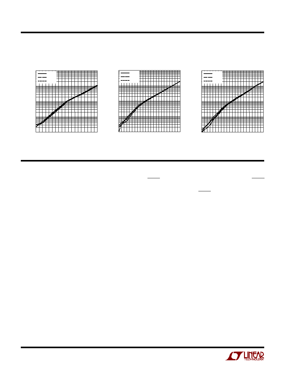
at 2700MHz
RF INPUT POWER (dBm)
10
PCTL REFERENCED DETECTOR OUTPUT VOLTAGE (mV)
100
1000
10000
22
10 6 2
6
2
10
14
1
18 14
4401 G04
75
°
C
25
°
C
30
°
C
TYPICAL PERFOR A CE CHARACTERISTICS
U
W
(LTC4401-1/LTC4401-2)
LTC4401-2 Detector Characteristics
at 900MHz
LTC4401-2 Detector Characteristics
at 1800MHz
RF INPUT POWER (dBm)
10
PCTL REFERENCED DETECTOR OUTPUT VOLTAGE (mV)
100
1000
10000
28
10
2
8
1
22
4
14
16
4401 G05
75
°
C
25
°
C
30
°
C
RF INPUT POWER (dBm)
10
PCTL REFERENCED DETECTOR OUTPUT VOLTAGE (mV)
100
1000
10000
26
14
8
2
4
10
16
1
20
4401 G06
75
°
C
25
°
C
30
°
C
5
LTC4401-1/LTC4401-2
sn4401 4401fs
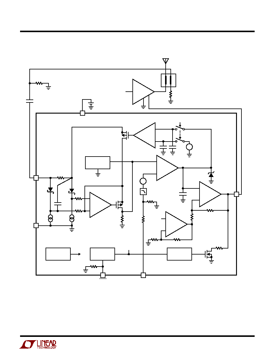
+
RF DET
+
GM
80mV
270kHz
FILTER
+
30k
22k
51k
30k
250
28pF
33pF
100
4401-1 BD
12
150k
60
µ
A
60
µ
A
RF
1
V
CC
Li-Ion
6
5
V
PCA
GND
PCTL
3
RF PA
RF IN
AZ
AUTOZERO
TXENB
+
+
CONTROL
4
SHDN
10
µ
s
DELAY
V
REF
50
2
68
V
REF
GAIN
COMPRESSION
CLAMP
C
C
BUFFER
38k
30k
33.4k
6k
30k
+
+
TXENB
LTC4401-1
VBG
BLOCK DIAGRA
W
(LTC4401-1)