 | ÐлекÑÑоннÑй компоненÑ: LTC4555 | СкаÑаÑÑ:  PDF PDF  ZIP ZIP |
LTC4555
LTC4555
1
4555f
APPLICATIO S
U
FEATURES
DESCRIPTIO
U
TYPICAL APPLICATIO
U
s
SIM Interface in 3G Cellular Telephones
s
Smart Card Readers
s
SIM Power Supply: 1.8V/3V at 50mA
s
Input Voltage Range: 3V to 6V
s
Controller Voltage Range: 1.2V to 4.4V
s
14kV ESD on all SIM Contact Pins
s
Meets all ETSI, IMT-2000 and ISO7816 SIM/Smart
Card Interface Requirements
s
Level Translators to 1.8V or 3V
s
20
µ
A Operating Current
s
Logic Controlled Shutdown (I
SD
< 1
µ
A)
s
Available in 0.8mm Tall, 3mm
×
3mm QFN Package
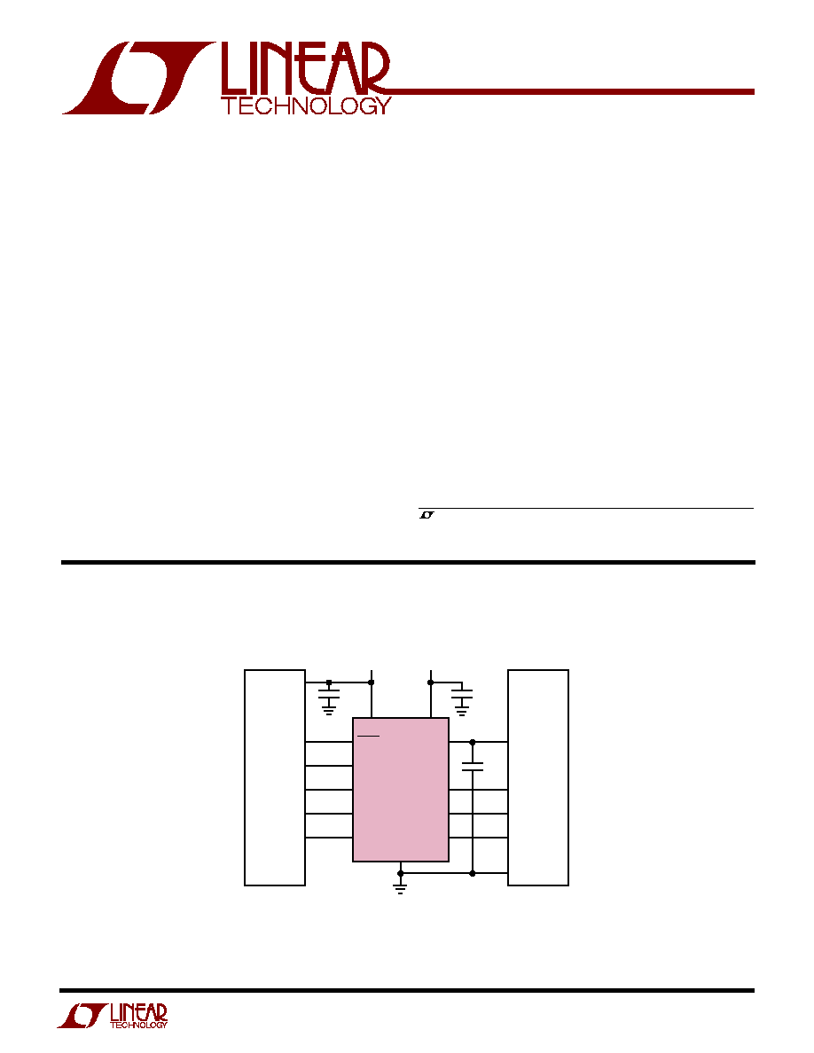
SIM Power Supply
and Level Translator
The LTC
®
4555 provides power conversion and signal level
shifting needed for low voltage 2.5G and 3G cellular
telephones to interface with 1.8V or 3V subscriber identity
modules (SIMs). The part meets all type approval require-
ments for 1.8V and 3V SIMs and smart cards. The part
contains an LDO linear regulator to supply SIM power at
either 1.8V or 3V from a 3V to 6V input. The output voltage
is selected with a single pin and up to 50mA of load current
can be supplied.
Internal level translators allow controllers operating with
supplies as low as 1.2V to interface with 1.8V or 3V smart
cards. Battery life is maximized by 20
µ
A operating current
and <1
µ
A shutdown current. Board area is minimized by
the 3mm
×
3mm leadless QFN package.
, LTC and LT are registered trademarks of Linear Technology Corporation.
SHDN
V
SEL
R
IN
C
IN
DATA
V
CC
RST
CLK
I/0
V
CC
RST
CLK
I/0
DV
CC
V
BAT
V
BAT
(3V TO 6V)
0.1
µ
F
0.1
µ
F
1
µ
F
CONTROLLER
V
CC
GND
GND
SIM/
SMART CARD
INTERFACE
LTC4555
4555 TA01
(1.2V TO 4.4V)
Typical SIM Interface
LTC4555
2
4555f
16 15 14 13
5
6
7
8
TOP VIEW
UD PACKAGE
16-LEAD (3mm
×
3mm) PLASTIC QFN
EXPOSED PAD IS GND
(MUST BE SOLDERED TO PCB)
9
10
11
12
4
3
2
1
SHDN
V
SEL
DV
CC
NC
NC
CLK
GND
RST
NC
DATA
R
IN
C
IN
V
BAT
NC
V
CC
I/O
V
BAT
, DV
CC
, V
CC
to GND ........................... 0.3V to 6.5V
Digital Inputs to GND ................................ 0.3V to 6.5V
CLK, RST, I/O to GND ..................... 0.3V to V
CC
+ 0.3V
V
CC
Short-Circuit Duration ................................... Infinite
Operating Temperature Range (Note 2) .. 40
°
C to 85
°
C
Storage Temperature Range ................. 65
°
C to 125
°
C
Lead Temperature (Soldering, 10 sec).................. 300
°
C
ORDER PART
NUMBER
T
JMAX
= 125
°
C,
JA
= 68
°
C/W,
JC
= 4.2
°
C/W
LTC4555EUD
ABSOLUTE AXI U
RATI GS
W
W
W
U
PACKAGE/ORDER I FOR ATIO
U
U
W
(Note 1)
ELECTRICAL CHARACTERISTICS
The
q
denotes the specifications which apply over the full operating
temperature range, otherwise specifications are at T
A
= 25
°
C.
Consult LTC Marketing for parts specified with wider operating temperature ranges.
PARAMETER
CONDITIONS
MIN
TYP
MAX
UNITS
V
BAT
Operating Voltage
q
3
6
V
V
BAT
Operating Current
I
CC
= 0mA
q
20
30
µ
A
V
BAT
Shutdown Current
SHDN = 0V
q
1
µ
A
DV
CC
Operating Voltage
q
1.2
4.4
V
DV
CC
Operating Current
f
CLK
= 1MHz
q
5
10
µ
A
DV
CC
Shutdown Current
SHDN = 0V
q
1
µ
A
DV
CC
Undervoltage Lockout
q
0.5
1.1
V
V
CC
Output Voltage
V
SEL
= DV
CC
, V
BAT
= 3V, I
VCC
= 50mA
2.8
V
V
SEL
= DV
CC
, V
BAT
= 3.3V to 6V, I
VCC
= 0mA to 50mA
q
2.8
3.0
3.2
V
V
SEL
= 0, V
BAT
= 2.6V to 6V, I
VCC
= 0mA to 50mA
q
1.7
1.8
1.9
V
V
CC
Short-Circuit Current
V
CC
Shorted to GND
60
110
175
mA
Controller Inputs/Outputs
Input Voltage Range
SHDN, V
SEL
, R
IN
, C
IN
, DATA
0
DV
CC
V
Input Current ( I
IH
/I
IL
)
SHDN, V
SEL
, R
IN
, C
IN
q
100
100
nA
High Input Threshold Voltage (V
IH
)
R
IN
, C
IN
q
0.7
×
DV
CC
V
Low Input Threshold Voltage (V
IL
)
R
IN
, C
IN
q
0.2
×
DV
CC
V
High Input Threshold Voltage (V
IH
)
SHDN, V
SEL
q
1
V
Low Input Threshold Voltage (V
IL
)
SHDN, V
SEL
q
0.4
V
High Level Input Current (I
IH
)
DATA
q
20
20
µ
A
Low Level Input Current (I
IL
)
DATA
q
1
mA
High Input Threshold Voltage (V
IH
)
DATA
q
DV
CC
- 0.6
V
Low Input Threshold Voltage (V
IL
)
DATA
q
0.4
V
High Level Output Voltage (V
OH
)
DATA I
OH
= 20
µ
A, I/O = V
CC
q
0.7
×
DV
CC
V
Low Level Output Voltage (V
OL
)
DATA I
OL
= 200
µ
A, I/O = 0V
q
0.4
V
DATA Pull-Up Resistance
Between DATA and DV
CC
13
20
30
k
LAAA
PART
MARKING
LTC4555
3
4555f
Note 1: Absolute Maximum Ratings are those values beyond which the life
of a device may be impaired.
Note 2: The LTC4555E is guaranteed to meet performance specifications
from 0
°
C to 70
°
C. Specifications over the 40
°
C to 85
°
C operating
ELECTRICAL CHARACTERISTICS
The
q
denotes the specifications which apply over the full operating
temperature range, otherwise specifications are at T
A
= 25
°
C.
temperature range are assured by design, characterization and correlation
with statistical process controls.
Note 3: Specification is guaranteed by design and not 100% tested in
production.
PARAMETER
CONDITIONS
MIN
TYP
MAX
UNITS
SIM Inputs/Outputs (V
CC
= 3V)
High Level Input Voltage (V
IH
)
I/O, I
IH
= 20
µ
A
q
0.7
×
V
CC
V
Low Level Input Voltage (V
IL
)
I/O, I
IL
= 1mA
q
0.4
V
High Level Output Voltage (V
OH
)
I/O, I
OH
= 20
µ
A, DATA =DV
CC
q
0.8
×
V
CC
V
Low Level Output Voltage (V
OL
)
I/O, I
OL
= 200
µ
A, DATA = 0V
q
0.4
V
High Level Output Voltage (V
OH
)
RST, CLK, I
OH
= 20
µ
A
q
0.9
×
V
CC
V
Low Level Output Voltage (V
OL
)
RST, CLK, I
OL
= 200
µ
A
q
0.4
V
I/O Pull-Up Resistance
Between I/O and V
CC
6.5
10
14
k
SIM Inputs/Outputs (V
CC
= 1.8V)
High Level Input Voltage (V
IH
)
I/O, I
IH
= 20
µ
A
q
0.7
×
V
CC
V
Low Level Input Voltage (V
IL
)
I/O, I
IL
= 1mA
q
0.2
×
V
CC
V
High Level Output Voltage (V
OH
)
I/O, I
OH
= 20
µ
A, DATA = DV
CC
q
0.8
×
V
CC
V
Low Level Output Voltage (V
OL
)
I/O, I
OL
= 200
µ
A, DATA = 0V
q
0.4
V
High Level Output Voltage (V
OH
)
RST, CLK, I
OH
= 20
µ
A
q
0.9
×
V
CC
V
Low Level Output Voltage (V
OL
)
RST, CLK, I
OL
= 200
µ
A
q
0.2
×
V
CC
V
I/O Pull-Up Resistance
Between I/O and V
CC
6.5
10
14
k
SIM Timing Parameters
CLK Rise/Fall Time
C
CLK
= 30pF, V
CC
= 3V
q
18
ns
C
CLK
= 30pF, V
CC
= 1.8V
q
50
ns
RST, I/O Rise/Fall Time
RST,I/O Loaded with 30pF, V
CC
= 1.8V/3V
q
1
µ
s
Max CLK Frequency
5
MHz
V
CC
Turn-On Time
SHDN = 1, (Note 3)
0.5
ms
V
CC
Discharge Time to 1V
SHDN = 0, (Note 3)
0.5
ms
LTC4555
4
4555f
U
U
U
PI FU CTIO S
SHDN (Pin 1): Controller Driven Shutdown Pin. This pin
should be high (DV
CC
) for normal operation and low to
activate a low current shutdown mode.
V
SEL
(Pin 2): V
CC
Voltage Select Pin. A low level selects
V
CC
= 1.8V while driving this pin to DV
CC
selects V
CC
= 3V.
DV
CC
(Pin 3): Supply Voltage for the Controller Side I/O
Pins (C
IN
, R
IN
, DATA). When below 1.1V, the V
CC
supply
is disabled, placing the LTC4555 in shutdown mode. This
pin should be bypassed with a 0.1
µ
F ceramic capacitor
close to the pin.
NC (Pins 4, 6, 12, 16): No Connect.
V
BAT
(Pin 5): V
CC
Supply Input. This pin can be between 3V
and 6V for normal operation. V
BAT
quiescent current
reduces to <1
µ
A in shutdown. This pin should be by-
passed with a 0.1
µ
F ceramic capacitor close to the pin.
V
CC
(Pin 7): SIM Card V
CC
Supply. A 1
µ
F low ESR
capacitor needs to be connected close to the V
CC
pin for
stable operation. This pin is discharged to GND during
shutdown.
I/O (Pin 8): SIM-Side Data I/O. The SIM card output must
be on an open drain driver capable of sourcing >1mA.
RST (Pin 9): Reset Output Pin for the SIM Card.
GND (Pin 10): Ground for the SIM and Controller. Proper
grounding and bypassing is required to meet 14kV ESD
specifications. Exposed pad must also be connected to
GND.
CLK (Pin 11): Clock Output Pin for the SIM Card. This pin
is pulled to ground during shutdown. Fast rising and
falling edges necessitate careful board layout for the CLK
node.
C
IN
(Pin 13): Clock Input from the Controller.
R
IN
(Pin 14): Reset Input from the Controller.
DATA (Pin 15): Controller Side Data I/O. This pin is used
for bidirectional data transfer. The controller output must
be an open-drain configuration. The open-drain output
must be capable of sinking greater than 1mA.
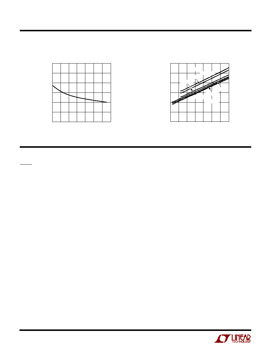
TYPICAL PERFOR A CE CHARACTERISTICS
U
W
I
BAT
vs V
BAT
V
CC
Short-Circuit Current
TEMPERATURE (
°
C)
40
SHORT-CIRCUIT CURRENT (mA)
170
150
130
110
90
70
50
20
60
4555 G01
20
0
40
80
100
T
A
= 40
°
C
V
BAT
(V)
2.5
I
BAT
(
µ
A)
22
20
18
16
14
12
10
4.0
5.0
4555 G02
3.0
3.5
4.5
5.5
6.0
V
CC
= 1.8V
V
CC
= 3V
T
A
= 25
°
C
T
A
= 85
°
C
T
A
= 85
°
C
T
A
= 25
°
C
T
A
= 40
°
C
LTC4555
5
4555f
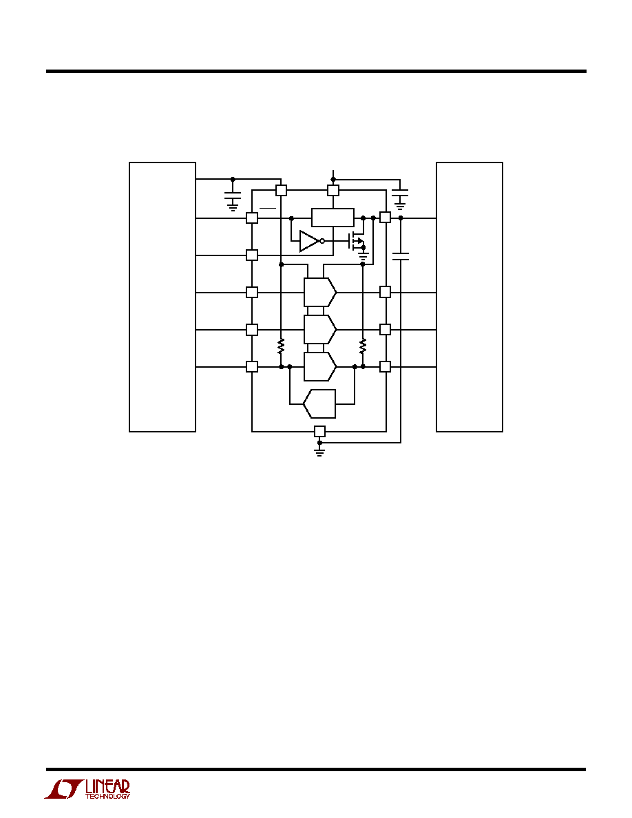
BLOCK DIAGRA
W
V
BAT
(3V TO 6V)
CELL PHONE
PROCESSOR
INTERFACE
SIM/
SMART CARD
INTERFACE
SHDN
V
SEL
R
IN
C
IN
DATA
RST
CLK
I/0
DV
CC
V
BAT
C1
1
µ
F
GND
50mA LDO
C3
0.1
µ
F
C2
0.1
µ
F
LTC4555
PROCESSOR
V
CC
SHUTDOWN
PIN
V
SIM
VOLTAGE
SELECT
RESET
FROM
PROCESSOR
CLOCK
FROM
PROCESSOR
DATA TO/
FROM SIM
1.8V/3V
AT 50mA
RESET
CLOCK
BIDIRECTIONAL
I/O
4555 BD
20k
10k
1
2
14
13
15
10
8
11
9
7
5
3
V
CC