 | ÐлекÑÑоннÑй компоненÑ: LTC5505 | СкаÑаÑÑ:  PDF PDF  ZIP ZIP |
5505-1/-2
LTC5505-1/LTC5505-2
1
5505f
s
Multimode Mobile Phone Products
s
PCS Devices
s
Wireless Data Modems
s
Wireless and Cable Infrastructure
s
RF Power Alarm
s
Envelope Detector
s
Internal Schottky Diode RF Detector with Two Input
Power Ranges:
LTC5505-1, 28dBm to 18dBm
LTC5505-2, 32dBm to 12dBm
s
Wide Input Frequency Range: 300MHz to 3GHz
(LTC5505-1); 300MHz to 3.5GHz (LTC5505-2)
s
Temperature Compensated
s
Buffered Detector Output
s
Wide V
CC
Range of 2.7V to 6V
s
Low Operating Current: 0.5mA
s
Low Shutdown Current: <2
µ
A
s
Low Profile (1mm) ThinSOT
TM
Package
RF Power Detector
with Buffered Output and >40dB
Dynamic Range
The LTC
®
5505-X is an RF power detector for RF applica-
tions operating in the 300MHz to 3.5GHz range. A tem-
perature compensated Schottky diode peak detector and
buffer amplifier are combined in a small 5-pin ThinSOT
package. The supply voltage range is optimized for opera-
tion from a single lithium-ion cell or 3xNiMH.
The RF input voltage is peak detected using an on-chip
Schottky diode. The detected voltage is buffered and
supplied to the V
OUT
pin. A power saving shutdown mode
reduces supply current to less than 2
µ
A.
The LTC5505-1 operates with input power levels from
28dBm to 18dBm. The LTC5505-2 operates with input
power levels from 32dBm to 12dBm.
, LTC and LT are registered trademarks of Linear Technology Corporation.
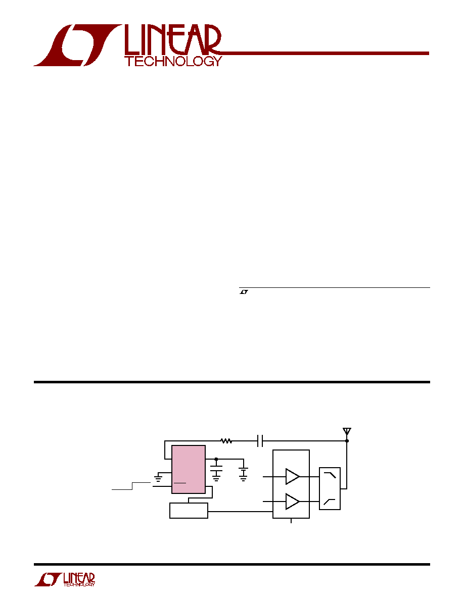
Dual Band Mobile Phone Tx Power Control
ThinSOT is a trademark of Linear Technology Corporation
APPLICATIO S
U
FEATURES
TYPICAL APPLICATIO
U
DESCRIPTIO
U
LTC5505-X
1
2
3
5
4
MOBILE PHONE
DSP
C2
0.1
µ
F
Li-Ion
V
CC
V
OUT
RF
IN
GND
SHDN
RF
DISABLE ENABLE
V
PC
Tx PA MODULE
CELL BAND
PCS BAND
BSE
5505 TA01
DIPLEXER
R1
100
C1
0.3pF
LTC5505-1/LTC5505-2
2
5505f
V
CC
, V
OUT
to GND .................................... 0.3V to 6.5V
RF Voltage
LTC5505-1 ................................... (V
CC
2.6V) to 7V
LTC5505-2 ................................... (V
CC
1.4V) to 7V
SHDN Voltage to GND ................ 0.3V to (V
CC
+ 0.3V)
I
VOUT
...................................................................... 5mA
Operating Temperature Range (Note 2) .. 40
°
C to 85
°
C
Maximum Junction Temperature ......................... 125
°
C
Storage Temperature Range ................ 65
°
C to 150
°
C
Lead Temperature (Soldering, 10 sec)................. 300
°
C
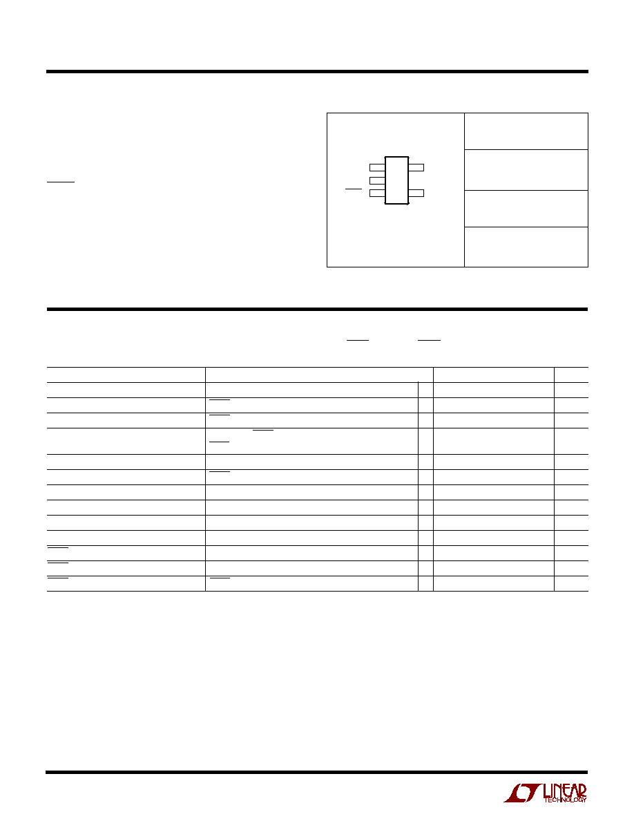
ORDER PART
NUMBER
S5 PART
MARKING
T
JMAX
= 125
°
C,
JA
= 250
°
C/W
LTXV
LTRW
LTC5505-1ES5
LTC5505-2ES5
ABSOLUTE AXI U
RATI GS
W
W
W
U
PACKAGE/ORDER I FOR ATIO
U
U
W
(Note 1)
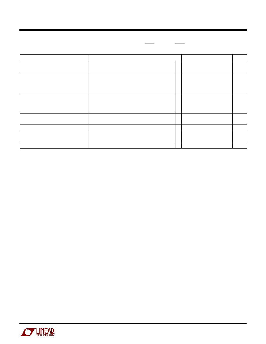
ELECTRICAL CHARACTERISTICS
The
q
denotes the specifications which apply over the full operating
temperature range, otherwise specifications are at T
A
= 25
°
C. V
CC
= 3.6V, SHDN = V
CC
= HI, SHDN = 0V = LO, RF Input Signal is Off,
unless otherwise noted.
PARAMETER
CONDITIONS
MIN
TYP
MAX
UNITS
V
CC
Operating Voltage
q
2.7
6
V
I
VCC
Shutdown Current
SHDN = LO
q
2
µ
A
I
VCC
Operating Current
SHDN = HI, I
VOUT
= 0mA
q
0.5
0.75
mA
V
OUT
V
OL
(No RF Input)
R
LOAD
= 2k, SHDN = HI, Enabled
170
260
350
mV
SHDN = LOW, Disabled
1
mV
V
OUT
Output Current
V
OUT
= 1.75V, V
CC
= 2.7V,
V
OUT
= 10mV
q
1
2
mA
V
OUT
Enable Time
SHDN = HI, C
LOAD
= 33pF, R
LOAD
= 2k
q
8
20
µ
s
V
OUT
Bandwidth
C
LOAD
= 33pF, R
LOAD
= 2k (Note 4)
4
MHz
V
OUT
Load Capacitance
(Note 7)
q
33
pF
V
OUT
Slew Rate
V
RFIN
= 2V Step, C
LOAD
= 33pF, R
LOAD
= 2k (Note 3)
10
V/
µ
s
V
OUT
Noise
V
CC
= 3V, Noise BW = 1.5MHz, 50
RF Input Termination
1.4
mV
P-P
SHDN Voltage, Chip Disabled
V
CC
= 2.7V to 6V
q
0.35
V
SHDN Voltage, Chip Enabled
V
CC
= 2.7V to 6V
q
1.4
V
SHDN Input Current
SHDN = 3.6V
q
24
40
µ
A
Consult LTC Marketing for parts specified with wider operating temperature ranges.
5 V
CC
4 V
OUT
RF
IN
1
TOP VIEW
S5 PACKAGE
5-LEAD PLASTIC SOT-23
GND 2
SHDN 3
LTC5505-1/LTC5505-2
3
5505f
Note 1: Absolute Maximum Ratings are those values beyond which the life
of a device may be impaired.
Note 2: Specifications over the 40
°
C to 85
°
C operating temperature
range are assured by design, characterization and correlation with
statistical process controls.
Note 3: The rise time at V
OUT
is measured between 0.5V and 1.5V.
Note 4: Bandwidth is calculated using the 10% to 90% rise time equation:
BW = 0.35/rise time.
Note 5: RF performance is tested at:
1800MHz, 14dBm, 14dBm (LTC5505-1)
1800MHz, 12dBm, 14dBm (LTC5505-2)
Note 6: For input RF power levels >16dBm, V
CC
minimum is 3V and an RF
input series resistor of 20
is required to limit the input current.
Note 7: Guaranteed by design.
ELECTRICAL CHARACTERISTICS
The
q
denotes the specifications which apply over the full operating
temperature range, otherwise specifications are at T
A
= 25
°
C. V
CC
= 3.6V, SHDN = V
CC
= HI, SHDN = 0V = LO, RF Input Signal is Off,
unless otherwise noted.
PARAMETER
CONDITIONS
MIN
TYP
MAX
UNITS
RF
IN
Input Frequency Range (LTC5505-1)
300 to 3000
MHz
(LTC5505-2)
300 to 3500
MHz
RF
IN
Input Power Range (LTC5505-1)
RF Frequency = 900MHz (Note 5, 6, 7) V
CC
= 2.7V to 6V
28 to 18
dBm
RF Frequency = 1800MHz (Note 5, 6, 7)V
CC
= 2.7V to 6V
26 to 18
dBm
RF Frequency = 2400MHz (Note 5, 7)V
CC
= 2.7V to 6V
24 to 16
dBm
RF Frequency = 2700MHz (Note 5, 7)V
CC
= 2.7V to 6V
22 to 16
dBm
RF
IN
Input Power Range (LTC5505-2)
RF Frequency = 900MHz (Note 5)
32 to 12
dBm
RF Frequency = 1800MHz (Note 5)
32 to 12
dBm
RF Frequency = 2400MHz (Note 5)
32 to 12
dBm
RF Frequency = 2700MHz (Note 5)
30 to 12
dBm
RF
IN
AC Input Resistance (LTC5505-1)
F = 850MHz
165
F = 1850MHz
20
RF
IN
Input Shunt Capacitance (LTC5505-1)
2
pF
RF
IN
AC Input Resistance (LTC5505-2)
F = 850MHz
165
F = 1850MHz
59
RF
IN
Input Shunt Capacitance (LTC5505-2)
1.3
pF
LTC5505-1/LTC5505-2
4
5505f
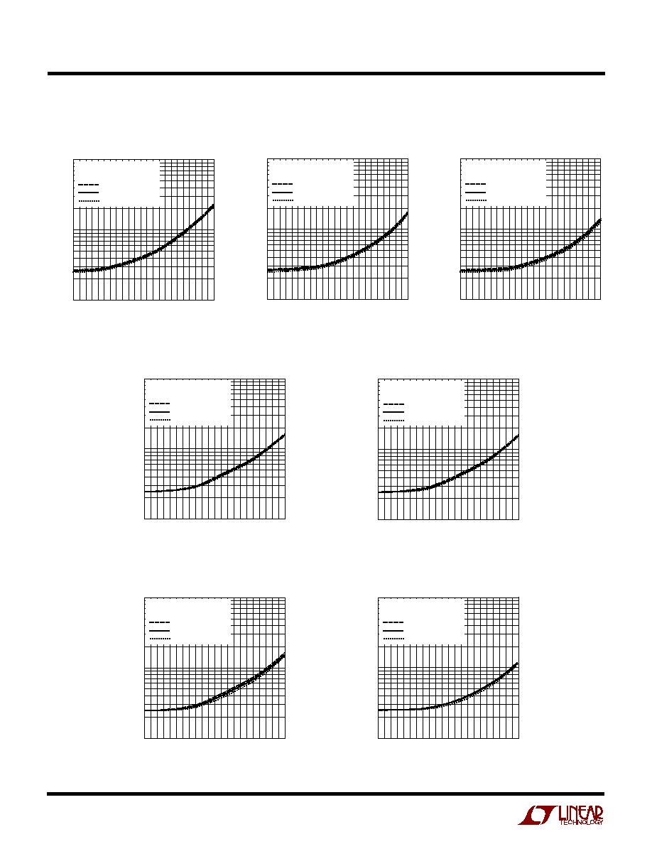
TYPICAL PERFOR A CE CHARACTERISTICS
U
W
LTC5505-1 Typical Detector
Characteristics, 0.85GHz
LTC5505-2 Typical Detector
Characteristics, 0.85GHz
LTC5505-1 Typical Detector
Characteristics, 2.45GHz
LTC5505-1 Typical Detector
Characteristics, 1.85GHz
RF INPUT POWER (dBm)
V
OUT
OUTPUT VOLTAGE (mV)
10000
5505 G01
100
1000
24
18
12
6
0
6
12
30
V
CC
= 2.7V TO 6V
0
SERIES TERMINATION
40
°
C
25
°
C
85
°
C
RF INPUT POWER (dBm)
V
OUT
OUTPUT VOLTAGE (mV)
10000
5505 G02
100
1000
24
18
12
6
0
6
12
30
V
CC
= 2.7V TO 6V
0
SERIES TERMINATION
40
°
C
25
°
C
85
°
C
RF INPUT POWER (dBm)
V
OUT
OUTPUT VOLTAGE (mV)
10000
5505 G03
100
1000
24 18
12
6
0
6
12
30
V
CC
= 2.7V TO 6V
0
SERIES TERMINATION
40
°
C
25
°
C
85
°
C
RF INPUT POWER (dBm)
V
OUT
OUTPUT VOLTAGE (mV)
10000
5505 G04
100
1000
26
20
14
8
2
4
10
32
V
CC
= 2.7V TO 6V
0
SERIES TERMINATION
40
°
C
25
°
C
85
°
C
LTC5505-2 Typical Detector
Characteristics, 2.45GHz
LTC5505-2 Typical Detector
Characteristics, 1.85GHz
RF INPUT POWER (dBm)
V
OUT
OUTPUT VOLTAGE (mV)
10000
5505 G05
100
1000
26
20
14
8
2
4
10
32
V
CC
= 2.7V TO 6V
0
SERIES TERMINATION
40
°
C
25
°
C
85
°
C
RF INPUT POWER (dBm)
V
OUT
OUTPUT VOLTAGE (mV)
10000
5505 G06
100
1000
26
20
14
8
2
4
10
32
V
CC
= 2.7V TO 6V
0
SERIES TERMINATION
40
°
C
25
°
C
85
°
C
LTC5505-2 Typical Detector
Characteristics, 3.5GHz
RF INPUT POWER (dBm)
V
OUT
OUTPUT VOLTAGE (mV)
10000
5505 G07
100
1000
26
20
14
8
2
4
10
32
V
CC
= 2.7V TO 6V
0
SERIES TERMINATION
40
°
C
25
°
C
85
°
C
LTC5505-1/LTC5505-2
5
5505f
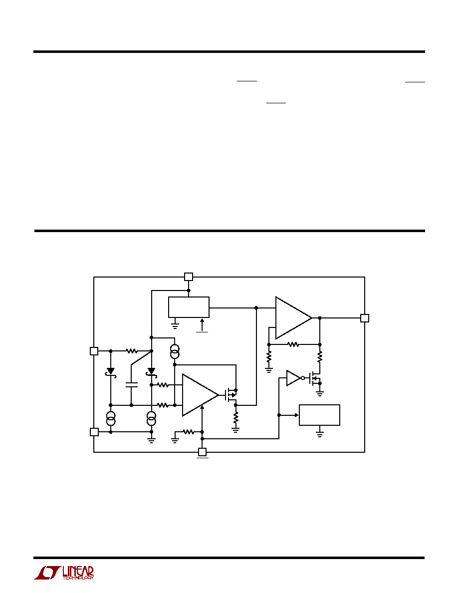
BLOCK DIAGRA
W
U
U
U
PI FU CTIO S
RF
IN
(Pin 1): RF Input Voltage. Referenced to V
CC
. An
external coupling capacitor to the RF source is required.
The frequency range is 300MHz to 3GHz. This pin has an
internal 250
termination, an internal Schottky diode
detector and peak detector capacitor. (See Note 6 in the
Electrical Characteristics.)
GND (Pin 2): System Ground.
SHDN (Pin 3): Shutdown Input. A logic low on the SHDN
pin places the part in shutdown mode. A logic high enables
the part. SHDN has an internal 150k pull down resistor to
ensure that the part is in shutdown when the drivers are in
a tri-state condition.
V
OUT
(Pin 4): Buffered and Level Shifted Detector Output
Voltage.
V
CC
(Pin 5): Power Supply Voltage, 2.7V to 6V. V
CC
should
be bypassed appropriately with ceramic capacitors.
+
+
5505 BD
GAIN
COMPRESSION
SHDN
28pF
V
OUT
SHDN
GND 2
3
4
5
BUFFER
250
RF DET
30k
30k
60
µ
A
60
µ
A
150k
22k
130mV
BIAS
100
100
RF
IN
V
CC
1