 | –≠–ª–µ–∫—Ç—Ä–æ–Ω–Ω—ã–π –∫–æ–º–ø–æ–Ω–µ–Ω—Ç: LTC6915 | –°–∫–∞—á–∞—Ç—å:  PDF PDF  ZIP ZIP |
LTC6915
1
6915f
APPLICATIO S
U
DESCRIPTIO
U
FEATURES
TYPICAL APPLICATIO
U
s
14 Levels of Programmable Gain
s
125dB CMRR Independent of Gain
s
Gain Accuracy 0.1% (Typ)
s
Maximum Offset Voltage of 10
µ
V
s
Maximum Offset Voltage Drift: 50nV/
∞
C
s
Rail-to-Rail Input and Output
s
Parallel or Serial (SPI) Interface for Gain Setting
s
Supply Operation: 2.7V to
±
5.5V
s
Typical Noise: 2.5
µ
V
P-P
(0.01Hz to 10Hz)
s
16-Lead SSOP and 12-Lead DFN Packages
s
Thermocouple Amplifiers
s
Electronic Scales
s
Medical Instrumentation
s
Strain Gauge Amplifier
s
High Resolution Data Acquisition
Zero Drift, Precision
Instrumentation Amplifier with
Digitally Programmable Gain
The LTC
Æ
6915 is a precision programmable gain instru-
mentation amplifier. The gain can be programmed to 0, 1,
2, 4, 8, 16, 32, 64, 128, 256, 512, 1024, 2048, or 4096
through a parallel or serial interface. The CMRR is typically
125dB with a dual 5V supply with any programmed gain.
The offset is below 10
µ
V with a temperature drift of less
than 50nV/
∞
C.
The LTC6915 uses charge balanced sampled data tech-
niques to convert a differential input voltage into a single
ended signal that is in turn amplified by a zero-drift
operational amplifier.
The differential inputs operate from rail-to-rail and the
single-ended output swings from rail-to-rail. The LTC6915
can be used in single power supply applications as low as
2.7V, or with dual
±
5V supplies. The LTC6915 is available
in a 16-lead SSOP package and a 12-lead DFN surface
mount package.
, LTC and LT are registered trademarks of Linear Technology Corporation.
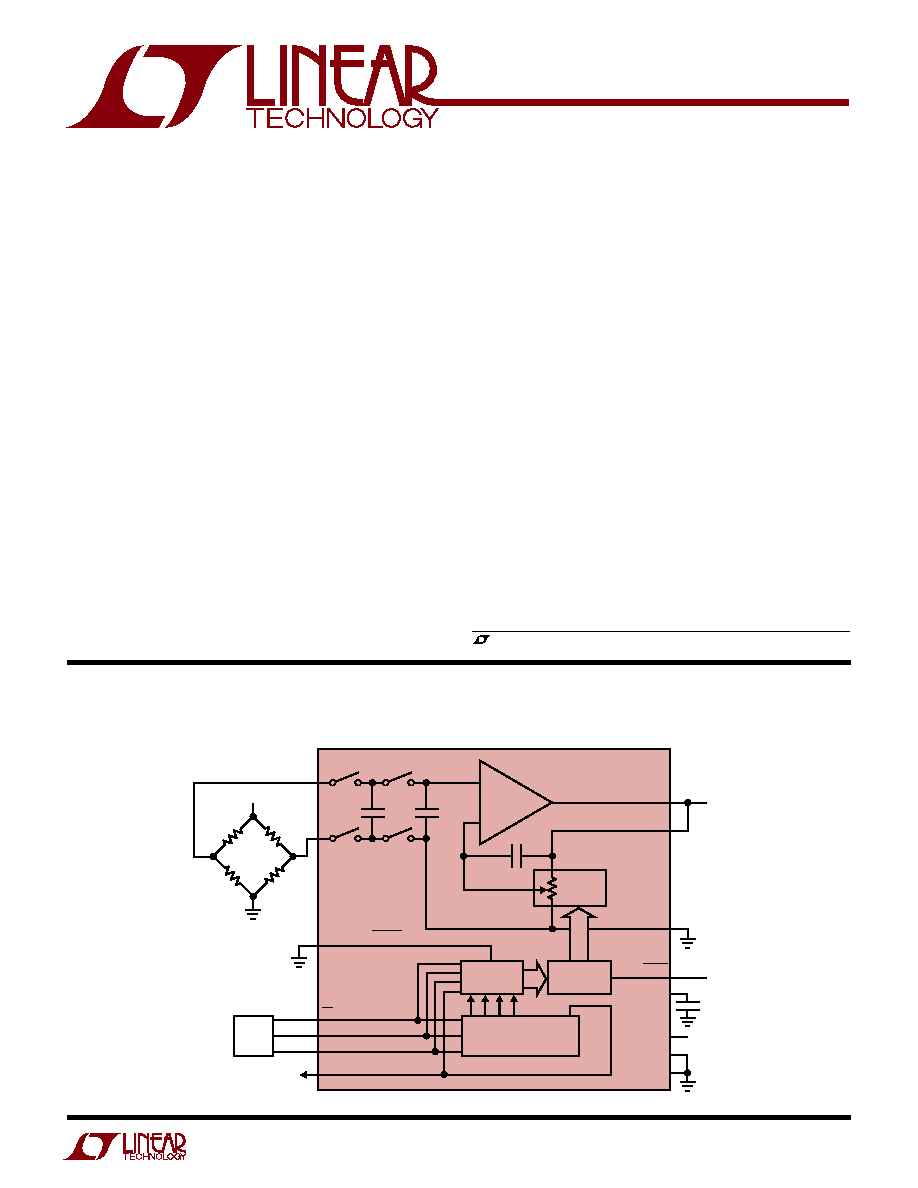
Differential Bridge Amplifier with Gain Programmed through the Serial Interface
≠
+
3V
RESISTOR
ARRAY
MUX
4-BIT
LATCH
Q0 Q1 Q2 Q3 Q4 Q5 Q6 Q7
8-BIT
SHIFT-REGISTER
HOLD_THRU
µ
P
TO OTHER
DEVICES
CS(D0)
D
IN
(D1)
CLK(D2)
D
OUT
(D3)
PARALLEL_SERIAL
IN
+
IN
_
3
2
11
6
7
8
9
R < 10k
C
S
C
H
LTC6915 SSOP PACKAGE
0.1
µ
F
V
+
V
≠
SHDN
DGND
13
5
16
10
1
4
OUT
REF
15
14
C
F
6915 TA01
SENSE
3V
LTC6915
2
6915f
Total Supply Voltage (V
+
to V
≠
) ............................... 11V
Input Current ......................................................
±
10mA
|V
IN
+
≠ V
REF
| ....................................................... 5.5V
|V
IN
≠
≠ V
REF
| ....................................................... 5.5V
|V
+
≠ V
DGND
| ....................................................... 5.5V
|V
DGND
≠ V
≠
| ....................................................... 5.5V
Digital Input Voltage ......................................... V
≠
to V
+
Operating Temperature Range
LTC6915C .............................................≠0
∞
C to 70
∞
C
ORDER PART
NUMBER
DFN PART
MARKING
T
JMAX
= 125
∞
C,
JA
= 160
∞
C/W
6915
6915I
LTC6915CDE
LTC6915IDE
ABSOLUTE AXI U
RATI GS
W
W
W
U
PACKAGE/ORDER I FOR ATIO
U
U
W
(Note 1)
ELECTRICAL CHARACTERISTICS
The
q
denotes the specifications which apply over the full operating
temperature range, otherwise specifications are at T
A
= 25
∞
C.
Consult LTC Marketing for parts specified with wider operating temperature ranges.
LTC6915I .............................................≠40
∞
C to 85
∞
C
LTC6915H .........................................≠40
∞
C to 125
∞
C
Junction Temperature
(GN Package) ................................................... 150
∞
C
(DFN Package).................................................. 125
∞
C
Storage Temperature
(GN Package) ....................................≠65
∞
C to 150
∞
C
(DFN Package)...................................≠65
∞
C to 125
∞
C
Lead Temperature (Soldering 10 sec)................... 300
∞
C
ORDER PART
NUMBER
GN PART
MARKING
6915
6915I
6915H
LTC6915CGN
LTC6915IGN
LTC6915HGN
T
JMAX
= 150
∞
C,
JA
= 135
∞
C/W
12
11
10
9
8
7
1
2
3
4
5
6
V
+
OUT
REF
PARALLEL_SERIAL
DGND
D
OUT
(D3)
IN
≠
IN
+
V
≠
CS(D0)
D
IN
(D1)
CLK(D2)
TOP VIEW
DE12 PACKAGE
12-LEAD (4mm
◊
3mm) PLASTIC DFN
UNDERSIDE METAL CONNECTED TO V≠
TOP VIEW
GN PACKAGE
16-LEAD NARROW PLASTIC SSOP
1
2
3
4
5
6
7
8
16
15
14
13
12
11
10
9
SHDN
IN
≠
IN
+
V
≠
HOLD_THRU
CS(D0)
D
IN
(D1)
CLK(D2)
V
+
OUT
SENSE
REF
NC
PARALLEL_SERIAL
DGND
D
OUT
(D3)
SYMBOL
PARAMETER
CONDITIONS
MIN
TYP
MAX
UNITS
V
+
= 3V, V
≠
= 0V, V
REF
= 200 mV
Gain Error (Note 2)
A
V
= 1 (R
L
=10k)
q
≠0.075
0
0.075
%
Gain Error (Note 2)
A
V
= 2 to 32 (R
L
= 10k)
q
≠0.5
0
0.5
%
Gain Error (Note 2)
A
V
= 64 to 1024 (R
L
= 10k)
q
≠0.6
≠0.1
0.6
%
Gain Error (Note 2)
A
V
= 2048, 4096 (R
L
= 10k)
q
≠1
≠0.2
1.0
%
Gain Nonlinearity
A
V
= 1
q
3
15
ppm
V
OS
Input Offset Voltage (Note 3)
V
CM
= 200mV
≠3
±
10
µ
V
Average Input Offset Drift (Note 3)
T
A
= ≠40
∞
C to 85
∞
C
q
±
50
nV/
∞
C
T
A
= 85
∞
C to 125
∞
C
q
±
100
nV/
∞
C
I
B
Average Input Bias Current (Note 4)
V
CM
= 1.2V
q
5
10
nA
I
OS
Average Input Offset Current (Note 4)
V
CM
= 1.2V
q
1.5
3
nA
LTC6915
3
6915f
The
q
denotes the specifications which apply over the full operating
temperature range, otherwise specifications are at T
A
= 25
∞
C.
ELECTRICAL CHARACTERISTICS
SYMBOL
PARAMETER
CONDITIONS
MIN
TYP
MAX
UNITS
V
+
= 3V, V
≠
= 0V, V
REF
= 200 mV
CMRR
Common Mode Rejection Ratio
A
V
= 1024, V
CM
= 0V to 3V, LTC6915C
q
100
119
dB
A
V
= 1024, V
CM
= 0.1V to 2.9V, LTC6915I
q
100
119
dB
A
V
= 1024, V
CM
= 0V to 3V, LTC6915I
q
95
119
dB
A
V
= 1024, V
CM
= 0.1V to 2.9V, LTC6915H
q
100
dB
A
V
= 1024, V
CM
= 0V to 2.97V, LTC6915H
q
85
dB
PSRR
Power Supply Rejection Ratio (Note 5)
V
S
= 2.7V to 6V
q
110
116
dB
Output Voltage Swing High
Sourcing 200
µ
A
q
2.95
2.98
V
(Referenced to V
≠
)
Sourcing 2mA
q
2.75
2.87
V
Output Voltage Swing Low
Sinking 200
µ
A
q
18
50
mV
(Referenced to V
≠
)
Sinking 2mA
q
130
300
mV
Supply Current, Parallel Mode
No Load at OUT, V
CM
= 200mV
q
0.88
1.3
mA
Supply Current, Serial Mode (Note 6)
No Load at OUT, Capacitive Load at
q
1.1
1.65
mA
D
OUT
(C
L
) = 15pF, Continuous CLK
Frequency = 4MHz, CS= LOW,
Gain Control Code = 0001
Supply Current Shutdown
V
SHDN
= 2.7V (Hardware Shutdown)
q
1
4
µ
A
V
SHDN
= 1V, Gain Control Code = 0000
q
125
180
µ
A
(Software Shutdown )
SHDN Input High
q
2.7
V
SHDN Input Low
q
1
V
SHDN and HOLD_THRU Input Current (Note 2)
q
5
µ
A
Internal Op Amp Gain Bandwidth
200
kHz
Slew Rate
0.2
V/
µ
s
Internal Sampling Frequency
≠0.5
3
kHz
V
+
= 5V, V
≠
= 0V, V
REF
= 200mV
Gain Error (Note 2)
A
V
= 1 (R
L
= 10k)
q
≠0.075
0
0.075
%
Gain Error (Note 2)
A
V
= 2 to 32 (R
L
= 10k)
q
≠0.5
0
0.5
%
Gain Error (Note 2)
A
V
= 64 to 1024 (R
L
= 10k)
q
≠0.6
≠0.1
0.6
%
Gain Error (Note 2)
A
V
= 2048, 4096 (R
L
= 10k)
q
≠1
≠0.2
1
%
Gain Nonlinearity
A
V
= 1
q
3
15
ppm
V
OS
Input Offset Voltage (Note 3)
V
CM
= 200mV
≠3
±
10
µ
V
Average Input Offset Drift (Note 3)
T
A
= ≠40
∞
C to 85
∞
C
q
±
50
nV/
∞
C
T
A
= 85
∞
C to 125
∞
C
±
100
nV/
∞
C
Average Input Bias Current (Note 4)
V
CM
= 1.2V
q
5
10
nA
I
OS
Average Input Offset Current (Note 4)
V
CM
= 1.2V
q
1.5
3
nA
CMRR
Common Mode Rejection Ratio
A
V
= 1024, V
CM
= 0V to 5V, LTC6915C
q
105
125
dB
A
V
= 1024, V
CM
= 0.1V to 4.9V, LTC6915I
q
105
125
dB
A
V
= 1024, V
CM
= 0V to 5V, LTC6915I
q
95
125
dB
A
V
= 1024, V
CM
= 0.1V to 4.9V, LTC6915H
q
100
dB
A
V
= 1024, V
CM
= 0V to 4.97V, LTC6915H
q
85
dB
PSRR
Power Supply Rejection Ratio (Note 5)
V
S
= 2.7V to 6V
q
110
116
dB
Output Voltage Swing High
Sourcing 200
µ
A
q
4.95
4.99
V
Sourcing 2mA
q
4.80
4.93
V
Output Voltage Swing Low
Sinking 200
µ
A
q
17
50
mV
Sinking 2mA
q
120
300
mV
LTC6915
4
6915f
The
q
denotes the specifications which apply over the full operating
temperature range, otherwise specifications are at T
A
= 25
∞
C.
ELECTRICAL CHARACTERISTICS
SYMBOL
PARAMETER
CONDITIONS
MIN
TYP
MAX
UNITS
V
+
= 5V, V
≠
= 0V, V
REF
= 200mV
Supply Current, Parallel Mode
No Load at OUT, V
CM
= 200mV
q
0.95
1.48
mA
Supply Current, Serial Mode (Note 6)
No Load at OUT, Capacitive Load at
q
1.4
2
mA
D
OUT
(C
L
) = 15pF, Continuous CLK
Frequency = 4MHz, CS = LOW,
Gain Control Code = 0001
Supply Current, Shutdown
V
SHDN
= 4.5V (Hardware Shutdown)
q
2
10
µ
A
V
SHDN
= 1V, Gain Control Code = 0000
q
135
200
µ
A
(Software Shutdown)
SHDN Input High
q
4.5
V
SHDN Input Low
q
1
V
SHDN and HOLD_THRU Input Current (Note 2)
q
5
µ
A
Internal Op Amp Gain Bandwidth
200
kHz
Slew Rate
0.2
V/
µ
s
Internal Sampling Frequency
3
kHz
V
+
= 5V, V
≠
= ≠5V, V
REF
= 0V
Gain Error (Note 2)
A
V
= 1 (R
L
= 10k)
q
≠0.075
0
0.075
%
Gain Error (Note 2)
A
V
= 2 to 32 (R
L
= 10k)
q
≠0.5
0
0.5
%
Gain Error (Note 2)
A
V
= 64 to 1024 (R
L
= 10k)
q
≠0.6
≠0.1
0.6
%
Gain Error (Note 2)
A
V
= 2048, 4096 (R
L
= 10k)
q
≠1
≠0.2
1
%
Gain Nonlinearity
A
V
= 1
q
3
15
ppm
V
OS
Input Offset Voltage (Note 3)
V
CM
= 0mV
5
±
20
nV
Average Input Offset Drift (Note 3)
T
A
= ≠40
∞
C to 85
∞
C
q
±
50
nV/
∞
C
T
A
= 85
∞
C to 125
∞
C
q
±
100
nV/
∞
C
I
OS
Average Input Bias Current (Note 4)
V
CM
= 1V
q
4
10
nA
Average Input Offset Current (Note 4)
V
CM
= 1V
q
1.5
3
nA
CMRR
Common Mode Rejection Ratio
A
V
= 1024, V
CM
= ≠5V to 5V, LTC6915C
q
105
123
dB
A
V
= 1024, V
CM
= ≠4.9V to 4.9V, LTC6915I
q
105
123
dB
A
V
= 1024, V
CM
= ≠5V to 5V, LTC6915I
q
100
123
dB
A
V
= 1024, V
CM
= ≠4.9V to 4.9V, LTC6915H
q
100
dB
A
V
= 1024, V
CM
= ≠5V to 4.97V, LTC6915H
q
90
dB
PSRR
Power Supply Rejection Ratio (Note 5)
V
S
= 2.7V to 11V
q
110
116
dB
Output Voltage Swing High
Sourcing 200
µ
A
q
4.97
4.99
V
Sourcing 2mA
q
4.90
4.96
V
Output Voltage Swing Low
Sinking 200
µ
A
q
≠4.98
≠4.92
mV
Sinking 2mA
q
≠4.90
≠4.70
mV
Supply Current, Parallel Mode
No Load, V
CM
= 200mV
q
1.1
1.6
mA
Supply Current, Serial Mode (Note 6)
No Load at OUT, Capacitive Load at
q
1.73
2.48
mA
D
OUT
(C
L
) = 15pF, Continuous CLK
Frequency = 4MHz, CS = LOW,
Gain Control Code = 0001
Supply Current, Shutdown
V
SHDN
= 4V (Hardware Shutdown)
q
25
µ
A
V
SHDN
= 1V, Gain Control Code = 0000
q
160
240
µ
A
(Software Shutdown )
SHDN Input High
q
4
V
SHDN Input Low
q
1
V
LTC6915
5
6915f
The
q
denotes the specifications which apply over the full operating
temperature range, otherwise specifications are at T
A
= 25
∞
C.
ELECTRICAL CHARACTERISTICS
SYMBOL
PARAMETER
CONDITIONS
MIN
TYP
MAX
UNITS
V
+
= 5V, V
≠
= ≠5V, V
REF
= 0V
SHDN and HOLD_THRU Input Current (Note 2)
q
5
µ
A
Internal Op Amp Gain Bandwidth
200
kHz
Slew Rate
0.2
V/
µ
s
Internal Sampling Frequency
3
kHz
Digital I/O, All Digital I/O Voltage Referenced to DGND
V
IH
Digital Input High Voltage
q
2.0
V
V
IL
Digital Input Low Voltage
q
0.8
V
V
OH
Digital Output High Voltage
Sourcing 500
µ
A
q
V
+
≠ 0.3
V
V
OL
Digital Output Low Voltage
Sinking 500
µ
A
q
0.3
V
Digital Input Leakage
V
+
= 5V, V
≠
= ≠5V, V
IN
= 0V to 5V
q
±
2
µ
A
Timing, V
+
= 2.7V to 4.5V, V
≠
= 0V (Note 7)
t
1
D
IN
Valid to CLK Setup
q
60
ns
t
2
D
IN
Valid to CLK Hold
q
0
ns
t
3
CLK Low
q
100
ns
t
4
CLK High
q
100
ns
t
5
CS/LD Pulse Width
q
60
ns
t
6
LSB CLK to CS/LD
q
60
ns
t
7
CS/LD Low to CLK
q
30
ns
t
8
D
OUT
Output Delay
C
L
= 15pF
q
125
ns
t
9
CLK Low to CS/LD Low
q
0
ns
Timing, V
+
= 4.5V to 5.5V, V
≠
= 0V (Note 7)
t
1
D
IN
Valid to CLK Setup
q
30
ns
t
2
D
IN
Valid to CLK Hold
q
0
ns
t
3
CLK Low
q
50
ns
t
4
CLK High
q
50
ns
t
5
CS/LD Pulse Width
q
40
ns
t
6
LSB CLK to CS/LD
q
40
ns
t
7
CS/LD Low to CLK
q
20
ns
t
8
D
OUT
Output Delay
C
L
= 15pF
q
85
ns
t
9
CLK Low to CS/LD Low
q
0
ns
Timing, Dual
±
4.5V to
±
5.5V Supplies (Note 7)
t
1
D
IN
Valid to CLK Setup
q
30
ns
t
2
D
IN
Valid to CLK Hold
q
0
ns
t
3
CLK High
q
50
ns
t
4
CLK Low
q
50
ns
t
5
CS/LD Pulse Width
q
40
ns
t
6
LSB CLK to CS/LD
q
40
ns
t
7
CS/LD Low to CLK
q
20
ns
t
8
D
OUT
Output Delay
C
L
= 15pF
q
85
ns
t
9
CLK Low to CS/LD Low
q
0
ns