 | –≠–ª–µ–∫—Ç—Ä–æ–Ω–Ω—ã–π –∫–æ–º–ø–æ–Ω–µ–Ω—Ç: LTC7541A | –°–∫–∞—á–∞—Ç—å:  PDF PDF  ZIP ZIP |
1
LTC7541A
Improved
Industry Standard CMOS
12-Bit Multiplying DAC
s
Improved Direct Replacement for AD7541A
and AD7541
s
4-Quadrant Multiplication
s
12-Bit End-Point Linearity:
±
0.5LSB DNL and INL
Over Temperature
s
All Grades Guaranteed Monotonic
s
Maximum Gain Error:
±
1LSB
s
Single 5V to 15V Supply
s
TTL and CMOS Logic Compatible
s
Reduced Sensitivity to Op Amp Offset
s
Low Power Consumption
s
Virtually Latch-Up Proof
s
Low Cost
The LTC
Æ
7541A is a 12-bit resolution multiplying digital-
to-analog converter (DAC).
Laser-trimmed thin-film resistors provide excellent abso-
lute accuracy. Precision matched resistors and CMOS
circuitry result in remarkable stability with temperature
and supply variations.
The LTC7541A is a superior pin compatible replacement
for the industry standard AD7541A/AD7541. Improve-
ments include better typical accuracy and stability and
reduced sensitivity to output amplifier offset. The LTC7541A
is also very resistant to latch-up.
In addition to 2-quadrant and 4-quadrant multiplying
configurations, the LTC7541A performs well in digitally
programmable gain and noninverting voltage output ap-
plications. Low cost, improved performance and versatil-
ity make the LTC7541A the best choice for many new
designs and for upgrading existing systems. Parts are
available in 18-pin PDIP and 18-pin SO Wide packages.
FEATURES
DESCRIPTIO
N
U
s
Motion Control Systems
s
Microprocessor-Controlled Calibration
s
Automatic Test Equipment
s
Programmable Gain Amplifiers
s
Digitally Controlled Filters
APPLICATIO
N
S
U
, LTC and LT are registered trademarks of Linear Technology Corporation.
TYPICAL APPLICATIO
N
U
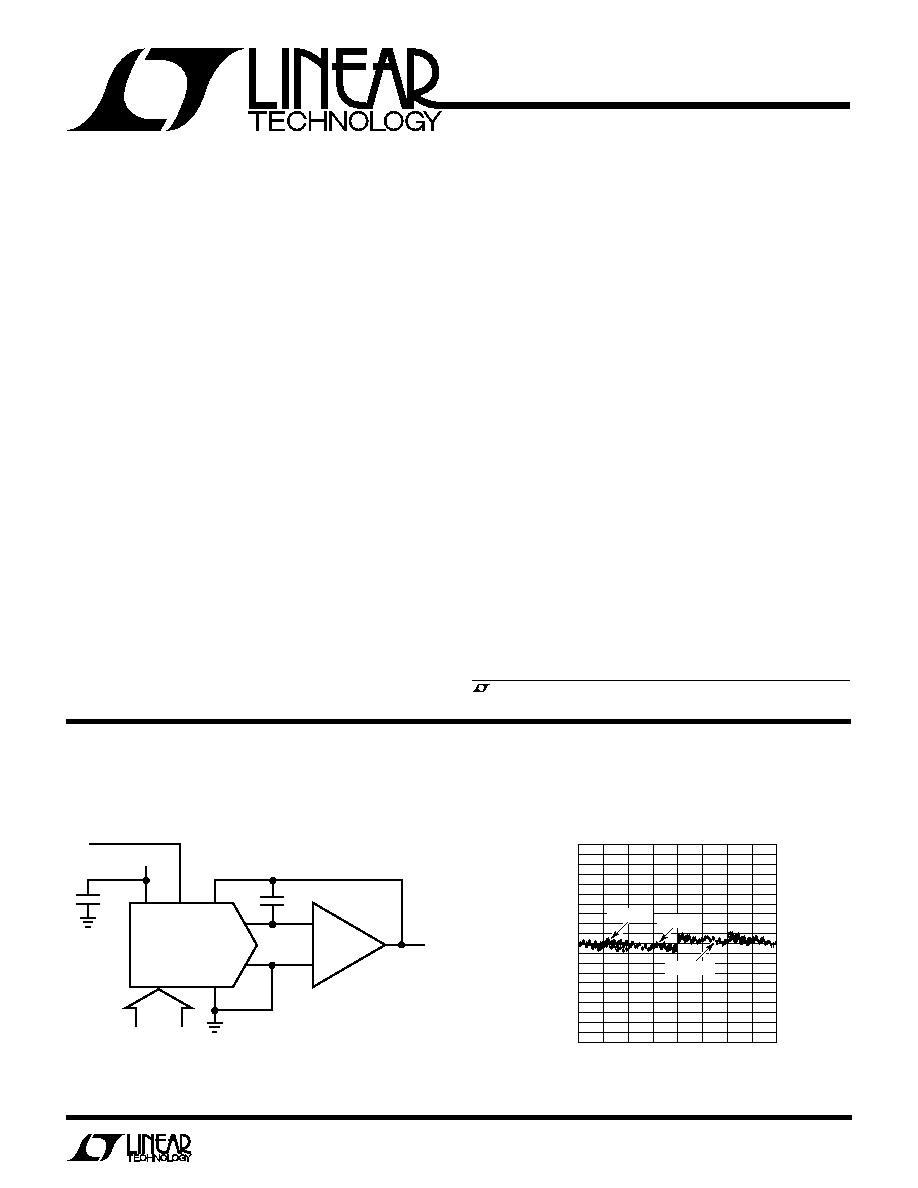
2-Quadrant Multiplying DAC Has Less Than
0.5LSB (Typ) Total Unadjusted Error
DIGITAL INPUT CODE
0
INTEGRAL NONLINEARITY (LSB)
4095
7541A TA02
1024
2048
3072
1.0
0.5
0
≠0.5
≠1.0
512
1536
2560
3584
T
A
= 85
∞
C
T
A
= 25
∞
C
T
A
= ≠40
∞
C
Integral Nonlinearity Over Temperature
V
DD
V
REF
LTC7541A
R
FB
GND
3
4 TO 15
2
16
15V
V
IN
17
18
1
OUT 1
33pF
V
OUT
7541 TA01
OUT 2
≠
+
0.1
µ
F
LT
Æ
1097
DIGITAL INPUTS

2
LTC7541A
ABSOLUTE
M
AXI
M
U
M
RATINGS
W
W
W
U
PACKAGE/ORDER I
N
FOR
M
ATIO
N
W
U
U
ELECTRICAL CHARACTERISTICS
V
DD
= 15V, V
REF
= 10V, OUT 1 = OUT 2 = GND = 0V, T
A
= T
MIN
to T
MAX
, unless otherwise specified.
V
DD
to GND ............................................... ≠ 0.5V to 17V
V
REF
to GND..........................................................
±
25V
R
FB
to GND ...........................................................
±
25V
Digital Inputs to GND .................. ≠ 0.5V to (V
DD
+ 0.5V)
OUT 1, OUT 2 to GND .................. ≠ 0.5V to (V
DD
+ 0.5V)
Power Dissipation ............................................. 450mW
(Derate 6mW/
∞
C Above 75
∞
C)
Maximum Junction Temperature ......... ≠ 65
∞
C to 125
∞
C
Operating Temperature Range
Commercial (J, K Versions).................. 0
∞
C to 70
∞
C
Industrial (B Version) ...................... ≠ 40
∞
C to 85
∞
C
Storage Temperature Range ................ ≠ 65
∞
C to 150
∞
C
Lead Temperature (Soldering, 10 sec) .................. 300
∞
C
LTC7541ABN
LTC7541ABSW
LTC7541AJN
LTC7541AKN
LTC7541AJSW
LTC7541AKSW
ORDER PART
NUMBER
Consult factory for Military grade parts.
T
JMAX
= 150
∞
C,
JA
= 100
∞
C/ W (N)
T
JMAX
= 150
∞
C,
JA
= 130
∞
C/ W (SW)
LTC7541AK/LTC7541AB
1
2
3
4
5
6
7
8
9
TOP VIEW
N PACKAGE
18-LEAD PDIP
SW PACKAGE
18-LEAD PLASTIC SO WIDE
18
17
16
15
14
13
12
11
10
OUT 1
OUT 2
GND
BIT 1 (MSB)
BIT 2
BIT 3
BIT 4
BIT 5
BIT 6
R
FB
V
REF
V
DD
BIT 12 (LSB)
BIT 11
BIT 10
BIT 9
BIT 8
BIT 7
LTC7541AJ
SYMBOL PARAMETER
CONDITIONS
MIN
TYP
MAX
MIN
TYP
MAX
UNITS
Accuracy
Resolution
q
12
12
Bits
INL
Integral Nonlinearity
(Note 1)
q
±
1
±
0.5
LSB
(Relative Accuracy)
DNL
Differential Nonlinearity
Guaranteed Monotonic, T
MIN
to T
MAX
q
±
1
±
0.5
LSB
GE
Gain Error
(Note 2)
T
A
= 25
∞
C
±
6
±
1
LSB
T
MIN
to T
MAX
q
±
8
±
2
LSB
Gain Temperature Coefficient
(Note 3)
q
1
5
1
5
ppm/
∞
C
I
LKG
Output Leakage Current
(Note 4)
T
A
= 25
∞
C
±
5
±
5
nA
T
MIN
to T
MAX
q
±
10
±
10
nA
PSRR
Power Supply Rejection
V
DD
= 15V
±
5%
q
±
0.002
±
0.002
%/%
Reference Input
R
REF
V
REF
Input Resistance
q
7
11
15
7
11
15
k
V
REF
Input Resistance
≠ 100
≠ 100
ppm/
∞
C
Temperature Coefficient
3
LTC7541A
V
DD
= 15V, V
REF
= 10V, OUT 1 = OUT 2 = GND = 0V, T
A
= T
MIN
to T
MAX
, unless otherwise specified.
The
q
denotes specifications which apply over the full operating
temperature range.
Note 1:
±
0.5LSB =
±
0.012% of full scale.
Note 2: Using internal feedback resistor.
Note 3: Guaranteed by design, not subject to test.
Note 4: I
OUT1
with all digital inputs = 0V or I
OUT2
with all digital
inputs = V
DD
.
Note 5: OUT 1 load = 100
in parallel with 13pF.
Note 6: Measured from digital input change to 90% of final analog value.
Digital inputs = 0V to V
DD
or V
DD
to 0V.
Note 7: V
REF
= 0V. All digital inputs 0V to V
DD
or V
DD
to 0V. Measured
using LT1363 as output amplifier.
ELECTRICAL CHARACTERISTICS
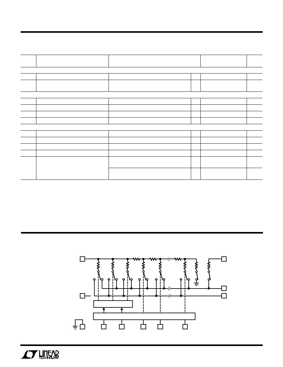
BLOCK DIAGRA
M
W
40k
10k
40k
20k
40k
20k
40k
20k
40k
40k
40k
DECODER
BIT 1
(MSB)
BIT 2
GND
V
DD
V
REF
R
FB
BIT 3
BIT 4
BIT 12
(LSB)
OUT 1
OUT 2
7541 BD
TTL/DTL/CMOS COMPATIBLE DIGITAL INPUTS
∑ ∑ ∑ ∑
Information furnished by Linear Technology Corporation is believed to be accurate and reliable.
However, no responsibility is assumed for its use. Linear Technology Corporation makes no represen-
tation that the interconnection of its circuits as described herein will not infringe on existing patent rights.
ALL GRADES
SYMBOL PARAMETER
CONDITIONS
MIN
TYP
MAX
UNIT
Power Supply
V
DD
Operating Supply Range
q
5
15
16
V
I
DD
Suppy Current
Digital Inputs = V
IH
or V
IL
q
2
mA
Digital Inputs = 0V or V
DD
q
100
µ
A
Digital Inputs
V
IH
Digital Input High Voltage
q
2.4
V
V
IL
Digital Input Low Voltage
q
0.8
V
I
IN
Digital Input Current
q
0.001
±
1
µ
A
C
IN
Digital Input Capacitance
(Note 3), V
IN
= 0V
q
8
pF
AC Performance
Propagation Delay
(Notes 5, 6)
100
ns
Digital-to-Analog Glitch Impulse
(Notes 5, 7)
1000
nV-sec
Multiplying Feedthrough Error
V
REF
=
±
10V, 10kHz Sinewave
1.0
mV
P-P
Output Current Settling Time
(Note 5), To 0.01% for Full-Scale Change
0.6
µ
s
C
OUT
Output Capacitance (Note 3)
Digital Inputs = V
IH
C
OUT1
q
200
pF
C
OUT2
q
70
pF
Digital Inputs = V
IL
C
OUT1
q
70
pF
C
OUT2
q
200
pF

4
LTC7541A
TYPICAL APPLICATIO
N
S
N
U
Unipolar Operation (2-Quadrant Multiplication)
RELATED PARTS
Bipolar Operation (4-Quadrant Multiplication)
V
DD
V
REF
LTC7541A
R
FB
GND
3
4 TO 15
2
16
15V
V
REF
≠ 10 TO 10V
17
18
1
OUT 1
33pF
R1
10k
V
OUT
7541 TA04
OUT 2
≠
+
0.1
µ
F
1/2 LT1112
≠
+
1/2 LT1112
DIGITAL INPUTS
Table 2. Bipolar Offset Binary Code Table
DIGITAL INPUT
V
REF
(2047/2048)
V
REF
(1/2048)
0V
≠V
REF
(1/2048)
≠V
REF
MSB
LSB
1111 1111 1111
1000 0000 0001
1000 0000 0000
0111 1111 1111
0000 0000 0000
ANALOG OUTPUT
V
OUT
R2
20k
R3
20k
V
DD
V
REF
LTC7541A
R
FB
GND
3
4 TO 15
2
16
15V
V
REF
≠ 10 TO 10V
17
18
1
OUT 1
33pF
V
OUT
7541 TA03
OUT 2
≠
+
0.1
µ
F
LT1097
DIGITAL INPUTS
Table 1. Unipolar Binary Code Table
DIGITAL INPUT
≠V
REF
(4095/4096)
≠V
REF
(2048/4096) = ≠V
REF
/ 2
≠V
REF
(1/4096)
0V
MSB
LSB
1111 1111 1111
1000 0000 0000
0000 0000 0001
0000 0000 0000
ANALOG OUTPUT
V
OUT
PART NUMBER
DESCRIPTION
COMMENTS
LTC1257
Complete Serial I/O V
OUT
12-Bit DAC
5V to 15V Single Supply in 8-Pin SO and PDIP
LTC1451/LTC1452/LTC1453
Complete Serial I/O V
OUT
12-Bit DACs
3V/5V Single Supply in 8-Pin SO and PDIP
LTC7543/LTC8143
Serial I/O Muliplying 12-Bit DACs
Clear Pin, Serial Data Output (LTC8143)
LTC8043
Serial Mulitplying 12-Bit DAC
8-Pin SO and PDIP
Linear Technology Corporation
1630 McCarthy Blvd., Milpitas, CA 95035-7487
(408) 432-1900
q
FAX
: (408) 434-0507
q
TELEX
: 499-3977
LT/GP 1195 6K ∑ PRINTED IN USA
©
LINEAR TECHNOLOGY CORPORATION 1995