
Features
n
Broad Bandwith Specified from 2 to 18 GHz
n
Integrated D.C. Bias Network
n
Exceptional Isolation to Loss Ratio
n
Rugged, Fully Monolithic, Glass Encapsulated
Construction
Description
The MA4SW410B-1 device is a SP4T Series-Shunt
Broad Band Switch with an Integrated Bias Network utilizing
M/A-COM's HMIC
TM
(Heterolithic Microwave Integrated Circuit)
Process, US Patent 5,268,310. This process allows the
incorporation of silicon pedestals that form series and shunt diodes
or vias by imbedding them in a low loss, low dispersion glass. This
hybrid combination of Silicon and Glass gives HMIC Switches
exceptional low loss and remarkable high isolation through
Ku Band frequencies.
Applications
These High Performance Switches are suitable for use in
Multi-Band ECM, Radar, and Instrumentation Control Circuits
where High Isolation to Insertion Loss Ratios are Required. With a
Standard +5 V/-5 V, TTL Controlled PIN Diode Driver, 80 nS
Switching Speeds are Achieved.
SP4T PIN Diode with
Integrated Bias Network
MA4SW410B
-
1
V 2.00
Outline Drawing
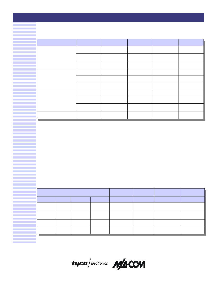
Parameter
Value
Operating Temperature
-65 �C to +125 �C
Storage Temperature
65 �C to +150 �C
RF C.W. Incident Power
(+/-20 mA)
+ 30 dBm
DC Bias Current
+/-40 mA
Absolute Maximum Ratings
1
@ TA = +25 �C (unless otherwise
specified)
1. Exceeding any of these values may result in permanent
damage
Nominal Die Dimensions
Dim
Inches
Min
Max
Min
Max
A
.085
.058
2.17
2.27
B
.106
.110
2.69
2.79
C
.048
.052
1.22
1.32
D
.007
.011
0.17
0.27
E
.033
.034
0.85
0.86
F
.057
.061
1.46
1.56
G
0.77
.081
1.96
2.06
H
0.46
.050
1.18
1.28
I
.024
.028
0.61
0.71
RF Bond
Pads
.007 X .005 REF.
.170 X .120 REF.
DC Bond
Pads
.005 X .005 REF.
.125 X .125 REF.
Thickness
005 REF.
.125 REF.
Millimeters
SP4T PIN Diode Switch with Integrated Bias Network
MA4SW410B-1
V 2.00
M/A-COM Inc. and its affiliates reserve the right to make changes to the product(s)
or information contained herein without notice.
Visit www.macom.com for additional data sheets and product information.
n
North America: Tel. (800) 366-2266
n
Asia/Pacific: Tel.+81-44-844-8296, Fax +81-44-844-8298
n
Europe: Tel. +44 (1344) 869 595, Fax+44 (1344) 300 020
2
1.
Typical Switching Speed measured from 10 % to 90 % of detected RF Voltage driven by TTL compatible drivers using RC Output
Spiking Network, where R = 50
�
200
, C = 390
�
560 pF.
Driver Connections for the MA4SW410B-1
Electrical Specifications @ T
A
= + 25 �C, +/- 10 mA Bias Current
(On-Wafer Measurements)
Parameters
Frequency
Minimum
Nominal
Maximum
Units
Insertion Loss
6 GHz
-
0.80
1.0
dB
12 GHz
-
1.00
1.2
dB
18 GHz
-
1.40
1.6
dB
Isolation
6 GHz
40
50
-
dB
12 GHz
35
40
-
dB
18 GHz
30
35
-
dB
6 GHz
-
10
-
dB
12 GHz
-
15
-
dB
18 GHz
-
10
-
dB
Switching Speed
1
-
-
80
-
nS
Input Return Loss
Operation of the MA4SW Series of PIN Switches is achieved by the Simultaneous Application of Negative DC
Current to the Low Loss Port and Positive DC current to the Remaining Isolated Switching Ports per the Driver
Connections Table. The control currents should be supplied by constant current sources. For Insertion Loss,
-10 mA bias results in approximately
�
2 V, and for Isolation ,+ 10 mA yields approximately +0.9 V at the
respective bias nodes. The Backside Area of the Die is the RF and DC Return Ground Plane.
Condition of
RF Output
Condition of
RF Output
Condition of
RF Output
Condition of
RF Output
B2
B3
B4
B5
J1-J2
J1-J3
J1-J4
-10 mA
+10 mA
+10 mA
+10 mA
Low Loss
Isolation
Isolation
Isolation
+10 mA
-10 mA
+10 mA
+10 mA
Isolation
Low Loss
Isolation
Isolation
+10 mA
+10 mA
-10 mA
+10 mA
Isolation
Isolation
Low Loss
Isolation
+10 mA
+10 mA
+10 mA
-10 mA
Isolation
Isolation
Isolation
Low Loss
Control Level (DC Current) at Port
J1-J5
Driver Connections for the MA4SW410B-1

SP4T PIN Diode Switch with Integrated Bias Network
MA4SW410B-1
V 2.00
M/A-COM Inc. and its affiliates reserve the right to make changes to the product(s)
or information contained herein without notice.
Visit www.macom.com for additional data sheets and product information.
n
North America: Tel. (800) 366-2266
n
Asia/Pacific: Tel.+81-44-844-8296, Fax +81-44-844-8298
n
Europe: Tel. +44 (1344) 869 595, Fax+44 (1344) 300 020
3
Mounting
These chips have TiPtAu back metal. They can be die
mounted with a gold-tin eutectic solder preform or electrically
conductive epoxy. Mounting surface must be clean and flat.
Eutectic Die Attachment
An 80/20 Gold-Tin eutectic solder preform is recommended
with a work surface temperature of 255 �C and a tool tip
temperature of 265 �C. When hot gas is applied, the tool tip
temperature should be 290 �C. The chip should not be exposed
to temperatures greater than 320 �C for more than 20 seconds.
No more than three seconds should be required for the attachment.
Electrically Conductive Epoxy
Die Attachment
Assembly should be preheated to 125-150 �C. A Controlled
thickness of 2 mils is recommended for best electrical and
thermal conductivity. A thin epoxy fillet should be visible
around the perimeter of the chip after placement. Cure epoxy
per manufacturer's schedule
.
Assembly Considerations
The following precautions should be observed for successful
assembly of the die.
Cleanliness
These chips should be handled in a clean environment. Do not
attempt to clean die after installation.
Electro-Static Sensitivity
The MA4SW410B-1 Series PIN Diode Switch is ESD, Class 1
sensitive. The proper ESD handling procedures should be
used.
Wire Bonding
Thermosonic wedge wire bonding using � x 3 mil sq. ribbon
or Ball Bonding using 1 mil diameter gold wire is recommended.
A stage temperature of 150 �C and a force of 18 to 22 grams
should be used. Ultrasonic energy should be adjusted to the
minimum required. RF bonds should be as short as possible.
MA4SW410B-1 Topology

SP4T PIN Diode Switch with Integrated Bias Network
MA4SW410B-1
V 2.00
M/A-COM Inc. and its affiliates reserve the right to make changes to the product(s)
or information contained herein without notice.
Visit www.macom.com for additional data sheets and product information.
n
North America: Tel. (800) 366-2266
n
Asia/Pacific: Tel.+81-44-844-8296, Fax +81-44-844-8298
n
Europe: Tel. +44 (1344) 869 595, Fax+44 (1344) 300 020
4
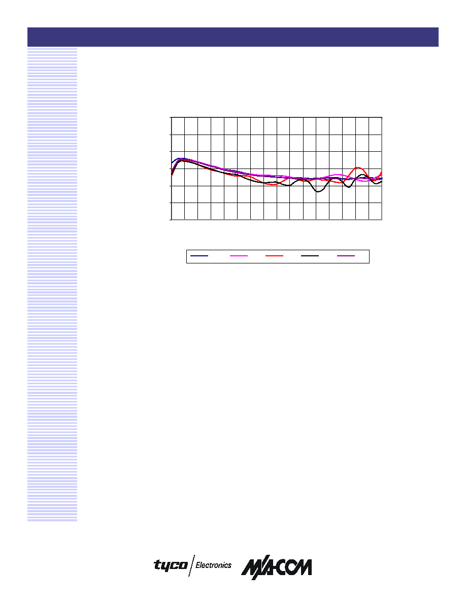
Microwave Performance
MA4SW410B-1 Typical Insertion Loss
-5
-4
-3
-2
-1
0
2
3
4
5
6
7
8
9
10
11
12
13
14
15
16
17
18
Frequency (Ghz)
dB
J1 to J2
J1 to J3
J1 to J4
J1 to J5
MA4SW410B-1 Typical Isolation
-70
-65
-60
-55
-50
-45
-40
-35
-30
-25
-20
-15
-10
-5
0
2
3
4
5
6
7
8
9
10
11
12
13
14
15
16
17
18
Frequency (GHz)
dB
J1 to J2
J1 to J3
J1 to J4
J1 to J5
SP4T PIN Diode Switch with Integrated Bias Network
MA4SW410B-1
V 2.00
M/A-COM Inc. and its affiliates reserve the right to make changes to the product(s)
or information contained herein without notice.
Visit www.macom.com for additional data sheets and product information.
n
North America: Tel. (800) 366-2266
n
Asia/Pacific: Tel.+81-44-844-8296, Fax +81-44-844-8298
n
Europe: Tel. +44 (1344) 869 595, Fax+44 (1344) 300 020
5
Microwave Performance
MA4SW410B-1 Typical Return Loss
-30
-25
-20
-15
-10
-5
0
2
3
4
5
6
7
8
9
10
11
12
13
14
15
16
17
18
Frequency (GHz)
dB
Input RL
J2 RL
J3 RL
J4 RL
J5 RL