 | –≠–ª–µ–∫—Ç—Ä–æ–Ω–Ω—ã–π –∫–æ–º–ø–æ–Ω–µ–Ω—Ç: MRF455 | –°–∫–∞—á–∞—Ç—å:  PDF PDF  ZIP ZIP |
The RF Line
NPN Silicon
RF Power Transistor
. . . designed for power amplifier applications in industrial, commercial and
amateur radio equipment to 30 MHz.
∑
Specified 12.5 Volt, 30 MHz Characteristics --
Output Power = 60 Watts
Minimum Gain = 13 dB
Efficiency = 55%
MATCHING PROCEDURE
In the push≠pull circuit configuration it is preferred that the transistors are
used as matched pairs to obtain optimum performance.
The matching procedure used by M/A-COM consists of measuring h
FE
at the
data sheet conditions and color coding the device to predetermined h
FE
ranges
within the normal h
FE
limits. A color dot is added to the marking on top of the cap.
Any two devices with the same color dot can be paired together to form a
matched set of units.
MAXIMUM RATINGS
Rating
Symbol
Value
Unit
Collector≠Emitter Voltage
V
CEO
18
Vdc
Collector≠Emitter Voltage
V
CES
36
Vdc
Emitter≠Base Voltage
V
EBO
4.0
Vdc
Collector Current -- Continuous
I
C
15
Adc
Total Device Dissipation @ T
C
= 25
∞
C
Derate above 25
∞
C
P
D
175
1.0
Watts
W/
∞
C
Storage Temperature Range
T
stg
≠65 to +150
∞
C
THERMAL CHARACTERISTICS
Characteristic
Symbol
Max
Unit
Thermal Resistance, Junction to Case
R
JC
1.0
∞
C/W
ELECTRICAL CHARACTERISTICS
(T
C
= 25
∞
C unless otherwise noted.)
Characteristic
Symbol
Min
Typ
Max
Unit
OFF CHARACTERISTICS
Collector≠Emitter Breakdown Voltage
(I
C
= 100 mAdc, I
B
= 0)
V
(BR)CEO
18
--
--
Vdc
Collector≠Emitter Breakdown Voltage
(I
C
= 50 mAdc, V
BE
= 0)
V
(BR)CES
36
--
--
Vdc
Emitter≠Base Breakdown Voltage
(I
E
= 10 mAdc, I
C
= 0)
V
(BR)EBO
4.0
--
--
Vdc
ON CHARACTERISTICS
DC Current Gain
(I
C
= 5.0 Adc, V
CE
= 5.0 Vdc)
h
FE
10
--
150
--
DYNAMIC CHARACTERISTICS
Output Capacitance
(V
CB
= 12.5 Vdc, I
E
= 0, f = 1.0 MHz)
C
ob
--
--
250
pF
(continued)
MRF455
60 W, 30 MHz
RF POWER
TRANSISTOR
NPN SILICON
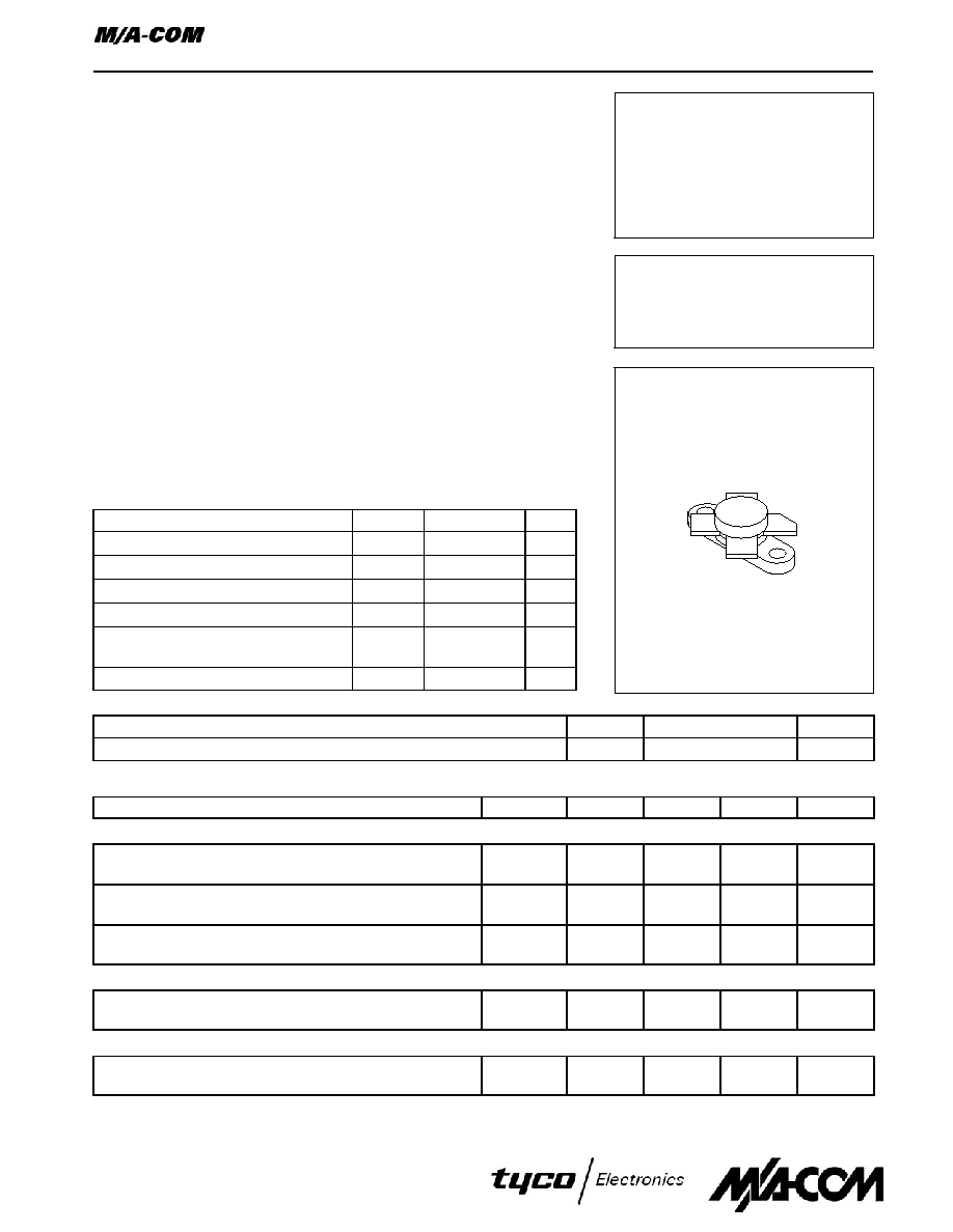
CASE 211≠07, STYLE 1
Order this document
by MRF455/D
SEMICONDUCTOR TECHNICAL DATA
1
ELECTRICAL CHARACTERISTICS -- continued
(T
C
= 25
∞
C unless otherwise noted.)
Characteristic
Unit
Max
Typ
Min
Symbol
FUNCTIONAL TESTS (Figure 1)
Common≠Emitter Amplifier Power Gain
(V
CC
= 12.5 Vdc, P
out
= 60 W, f = 30 MHz)
G
pe
13
--
--
dB
Collector Efficiency
(V
CC
= 12.5 Vdc, P
out
= 60 W, f = 30 MHz)
55
--
--
%
Series Equivalent Input Impedance
(V
CC
= 12.5 Vdc, P
out
= 60 W, f = 30 MHz)
Z
in
--
1.66≠j.844
--
Ohms
Series Equivalent Output Impedance
(V
CC
= 12.5 Vdc, P
out
= 60 W, f = 30 MHz)
Z
out
--
1.73≠j.188
--
Ohms
Parallel Equivalent Input Impedance
(V
CC
= 12.5 Vdc, P
out
= 60 W, f = 30 MHz)
Z
in
--
2.09/1030
--
/pF
Parallel Equivalent Output Impedance
(V
CC
= 12.5 Vdc, P
out
= 60 W, f = 30 MHz)
Z
out
--
1.75/330
--
/pF
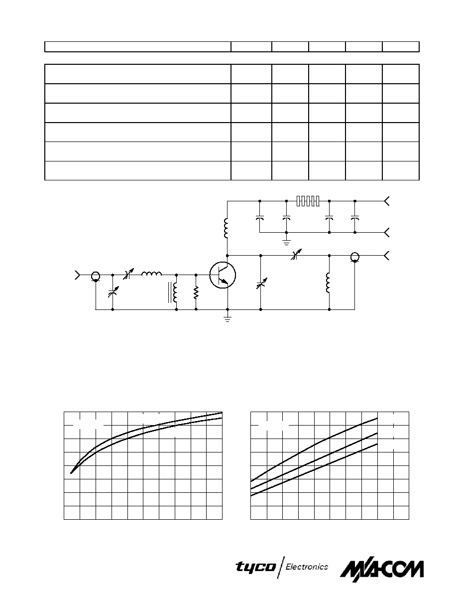
Figure 1. 30 MHz Test Circuit Schematic
f = 30 MHz
P
, OUTPUT
POWER (W
A
TTS)
out
80
P
in
, INPUT POWER (WATTS)
0
70
60
50
40
0
1
2
3
4
5
30
20
10
P
, OUTPUT
POWER (W
A
TTS)
out
V
CC
, SUPPLY VOLTAGE (VOLTS)
0.5
1.5
2.5
3.5
4.5
V
CC
= 13.6 V
80
70
60
50
40
30
20
10
f = 30 MHz
12.5 V
P
in
= 3.5 V
1 W
1.75 W
8
10
12
14
16
18
9
11
13
15
17
L3
R1
C5
C6
C7
C8
RF OUTPUT
L4
C4
C1
C2
L2
DUT
C3
L1
-
+
12.5 Vdc
L5
RF INPUT
C1, C2, C4 -- ARCO 469
C3 -- ARCO 466
C5 -- 1000 pF, UNELCO
C6, C7 -- 0.1
µ
F Disc Ceramic
C8 -- 1000
µ
F/15 V Electrolytic
R1 -- 10 Ohm/1.0 Watt, Carbon
L1 -- 3 Turns, #18 AWG, 5/16
I.D., 5/16
Long
L2 -- VK200≠20/4B, FERROXCUBE
L3 -- 12 Turns, #18 AWG Enameled Wire, 1/4
I.D., Close Wound
L4 -- 3 Turns 1/8
O.D. Copper Tubing, 3/8
I.D., 3/4
Long
L5 -- 7 FERRITE Beads, FERROXCUBE #56≠590≠65/3B
90
Figure 2. Output Power versus Input Power
Figure 3. Output Power versus Supply Voltage
2
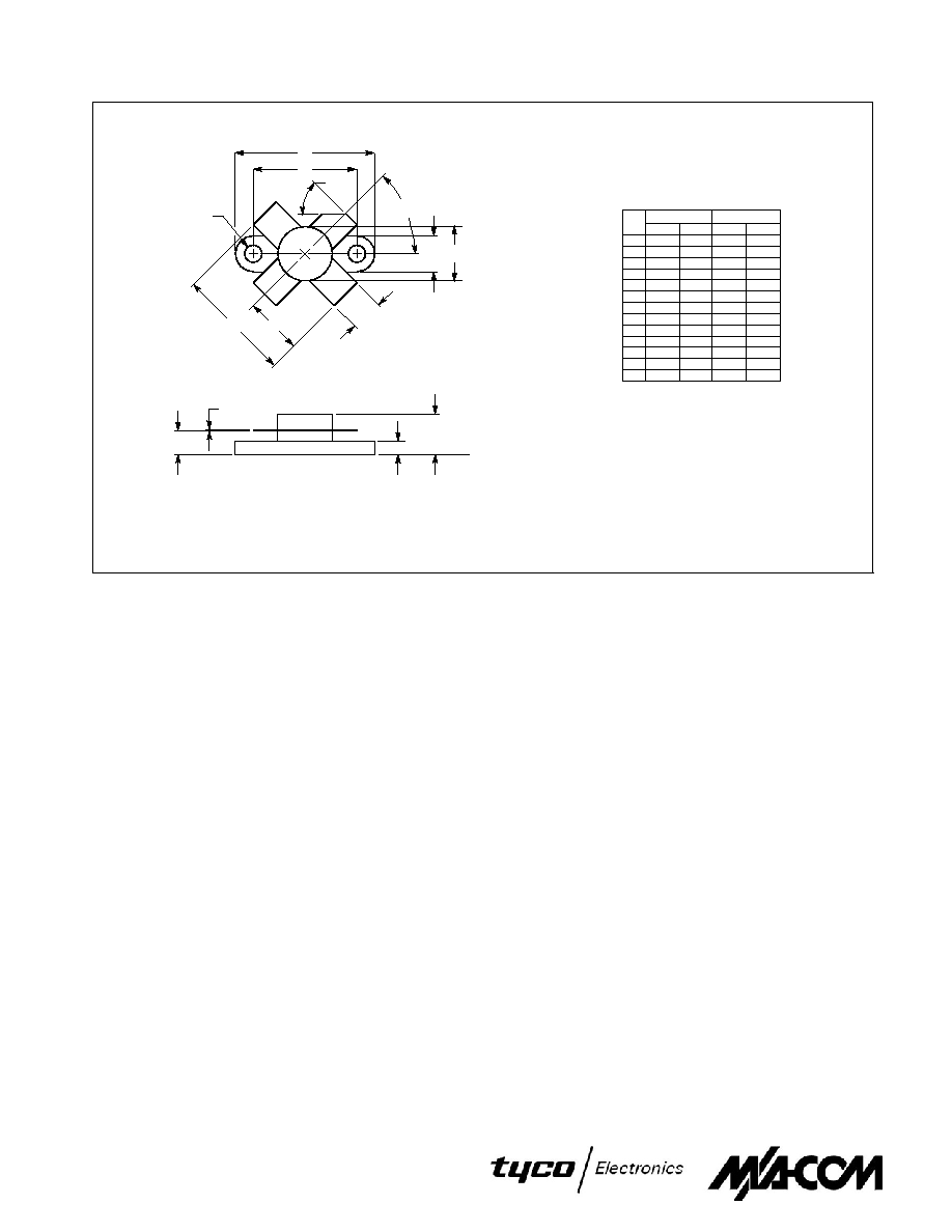
PACKAGE DIMENSIONS
CASE 211≠07
ISSUE N
NOTES:
1. DIMENSIONING AND TOLERANCING PER ANSI
Y14.5M, 1982.
2. CONTROLLING DIMENSION: INCH.
A
U
M
M
Q
R
B
1
4
3
2
D
K
E
SEATING
PLANE
C
J
H
S
DIM
MIN
MAX
MIN
MAX
MILLIMETERS
INCHES
A
0.960
0.990
24.39
25.14
B
0.370
0.390
9.40
9.90
C
0.229
0.281
5.82
7.13
D
0.215
0.235
5.47
5.96
E
0.085
0.105
2.16
2.66
H
0.150
0.108
3.81
4.57
J
0.004
0.006
0.11
0.15
K
0.395
0.405
10.04
10.28
M
40
50
40
50
Q
0.113
0.130
2.88
3.30
R
0.245
0.255
6.23
6.47
S
0.790
0.810
20.07
20.57
U
0.720
0.730
18.29
18.54
_
_
_
_
STYLE 1:
PIN 1. EMITTER
2. BASE
3. EMITTER
4. COLLECTOR
3
Specifications subject to change without notice.
n
North America: Tel. (800) 366-2266, Fax (800) 618-8883
n
Asia/Pacific: Tel.+81-44-844-8296, Fax +81-44-844-8298
n
Europe: Tel. +44 (1344) 869 595, Fax+44 (1344) 300 020
Visit www.macom.com for additional data sheets and product information.