 | –≠–ª–µ–∫—Ç—Ä–æ–Ω–Ω—ã–π –∫–æ–º–ø–æ–Ω–µ–Ω—Ç: MAS9191A | –°–∫–∞—á–∞—Ç—å:  PDF PDF  ZIP ZIP |
1
DA9191A.000
July 31, 1997
0$6$
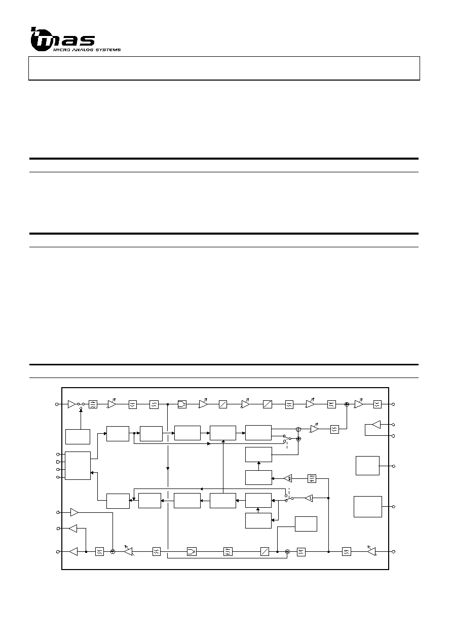
6LQJOH &KLS $036(7$&61$036 $XGLR'DWD 3URFHVVRU
∑
6LQJOH FKLS VROXWLRQ IRU DOO DXGLR DQG GDWD SURFHVVLQJ
∑
/RZ SRZHU FRQVXPSWLRQ ZLWK VHYHUDO SRZHU GRZQ PRGHV
∑
6$7 GHFRGLQJ DQG WUDQVSRQGLQJ FLUFXLWU\
∑
6LPSOH ZLUH VHULDO LQWHUIDFH
'(6&5,37,21
The MAS9191A is a high integration BeCMOS IC for
implementing the audio and data signal processing in
AMPS, ETACS or NAMPS cellular phones. The
power consumption of the device is very low due to
several automatic and software controlled power
down modes as well as the low power characteristics
of the BeCMOS process. DTMF receiver is also
included to enable answering machine functions for
the cellular phone. Only a minimal number of external
components are needed to meet typical baseband
requirements.
)($785(6
$33/,&$7,216
∑
Voice signal processing including compressor,
expander, de-emphasis and pre-emphasis filters
and digital gain adjustments
∑
DTMF and ST generators and DTMF receiver
∑
Busy/Idle extraction and arbitration with TX block,
voting, BCH, data buffering and framing, DCC
coding with hardware
∑
Three 8-bit DACs and two operational amplifiers
∑
On-chip oscillator with clock output for uP
∑
3.3V or 5V operation with low power
consumption(RX block at 2mA/3.3V)
∑
64-pin TQFP package, -40..85
o
C operation range
∑
AMPS/ETACS Cellular phone
∑
NAMPS Cellular phone
%/2&. ',$*5$0
MIC
Serial
Interface
TX
Buffer
DCC
Conversion
Framing
RX
Buffer
DTMF
Receiver
Voting
Manchester
Decoder
DPLL
SCL
STB
SRxD
STxD
RX
TX
EXPANDER
BANDPASS
FILTER
DE-EMPHASIS
GAIN
CONTROL
COMPARATOR
GAIN
CONTROL
COMPRESSOR
PRE-EMPHASIS
LIMITER
LOWPASS
FI LTER
Manchester
coding
BCH
Coding
SAT
Generation
Frame
Decoding
SAT
Detection
COMPARATOR
DTMF
Genera tor
SIDETONE
SPEAKER
3
8-bit
DACs
2 Utility
Operational
Amplifiers
AMPLIFIER
AMPLIFIER
A NTI -
ALI ASING
BUZZER
AMPLIFIER
XSTAL1
XSTAL2
LOWPASS
FI LTER
LO WPASS
FI LTER
LO WP ASS
FILTER
GAIN
CONTRO L
GAIN
CONTRO L
GAIN
CONTROL
GAIN
CONTROL
GAIN
CONTRO L
AMPLIFIER
AMPLIFIER
LO WP ASS
FI LTER
LO WP ASS
FI LTER
LOWPASS
FILTER
LOWPASS
FILTER
GAIN
CONTRO L
HIGHPA SS
FILTER
LOWPASS
FILTER
BCH
Decoding
BU
SY
/ I
D
L
E
SIGNALLING
TONE
BANDP ASS
FILTER
SYS1 (NAMPS)
SYS1 (NAMPS )
2
DA9191A.000
July 31, 1997
3,1 &21),*85$7,21
$*1'
7;
7$8'287
7$8',1
/3),1
96$7
9'$7
7;$&&287
&287
&$03,
&:&,1
&$03
&203,1
0,&287
'
$
&
2
8
7
'
$
&
2
8
7
'
$
&
2
8
7
;
,
1
7
%
8
6
<
7
;
2
1
(,15
6
,
'
(
7
2
1
(
6
,
'
(
)
%
(
$
5
3
(
$
5
3
(
;
7
(
5
3
%
8
=
2
8
7
%
8
=
)
%
6
5
[
'
67*7
(67
5$8',1
5;$&&287
(;3287
7;$&&,1
35(,1
5;$&&,1
(:&,1
($03287
(;3,1
9'$5
96$5
5%3)287
5%3),1
'(287
95()
9
'
'
;
7
$
/
;
7
$
/
9
6
6
7
;
&
7
5
/
&
/
.
2
8
7
7
(
6
7
7
(
6
7
$
/
3
5
;
0
,
&
6
*
1
'
6
&
/
;
5
(
6
(
7
(
;
7
0
,
&
0
,
&
)
%
0
,
&
6
7
%
6
7
[
'
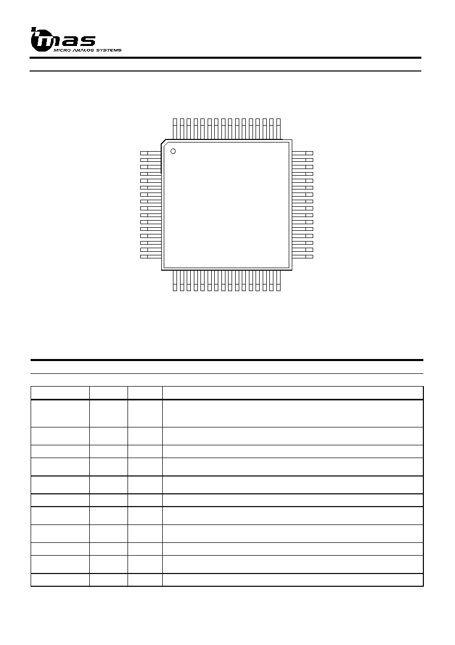
TQFP64 package
3,1 '(6&5,37,21
3LQ QDPH
3LQ
7\SH
)XQFWLRQ
AGND
1
AO
Signal ground. The signal ground is generated internally and is equal to
V
DD
/2. The analog ground needs an external capacitor connected to
system ground.
TX
2
AO
Transmitted data signal output. Connect this output through a 22nF
capacitor to the transmitter.
TAUDOUT
3
AO
TX audio output from the TX audio block..
TAUDIN
4
AI
TX audio input. The input for the TX audio signal, normally connected
through a 22nF capacitor to TAUDOUT
LPFIN
5
AI
Input for TX limiter, lowpass filter or GC6 depending on the position of
switches S15 and S16. The pin is normally left unconnected.
VSAT
6
G
Ground for TX. Connect to system ground.
VDAT
7
P
Power supply for TX block. Use a bypass capacitor between pins VSAT
and VDAT.
TXACCIN
8
AI
TX block extra Op Amp input. See application note in the APPLICATIONS
section.
TXACCOUT
9
AO
TX block Op Amp output.
PREIN
10
AI
Pre-emphasis filter input. Filter has a +6dB/octave (±1dB) frequency
response in the range 300Hz...3kHz.
COUT
11
AO
Compressor output signal. The compression ratio is 2:1

3
DA9191A.000
July 31, 1997
3,1 '(6&5,37,21
3LQ QDPH
3LQ
7\SH
)XQFWLRQ
CAMP2I
12
AI
Compressor 2nd amplifier input as well as GC4 input. Use an external
22nF capacitor between COUT and this pin.
CWCIN
13
AI
Compressor window comparator input. Use an external 22nF capacitor
between CAMP2O and this pin.
CAMP2O
14
AO
Compressor 2nd amplifier output.
COMPIN
15
AI
Compressor input. The input is connected through a 22nF capacitor to
MICOUT.
MICOUT
16
AO
Microphone amplifier output. See COMPIN. This output is used as a
source for the side tone and for detection of the TX audio level.
MICSGND
17
AO
Microphone signal ground. This is the internal signal ground V
DD
/2. If noise
appears on the microphone signal an external capacitor may be needed
between this pin and system ground.
MIC
18
AI
Microphone amplifier input. Using this pin and the MICFB output the
microphone amplifier frequency response can be adjusted according to the
microphone used. The level at this input should be in the range
5..10mVrms. The maximum gain of the microphone amplifier is 30 dB.
MICFB
19
AO
Microphone amplifier feedback output
EXTMIC
20
AI
External microphone input. The level should be 100mVrms at 1kHz.
XRESET
21
I
Master reset. Active low.
SCL
22
I
Serial interface clock input. The data is transferred in both directions at the
rising edge of this signal.
STB
23
I
Serial interface strobe signal. With strobe signal the MAS9191A stores the
given address from the serial interface buffer and enters the data mode.
The serial interface stays in the data mode until eight SCL pulses are
received after the strobe signal.
STxD
24
O
Serial interface transmit data output.
SRxD
25
I
Serial interface receive data input
BUZFB
26
AI
Buzzer feedback is the input for the buzzer driver.
BUZOUT
27
AO
Buzzer output.
EXTERP
28
AO
Output for external accessories
EARP1
29
AO
Earpiece differential outputs of earpiece amplifier. The outputs are capable
of driving a ceramic earpiece directly.
EARP2
30
AO
SIDEFB
31
AO
Side tone feedback output
SIDETONE
32
AI
Side tone input. The level of the side tone is controlled with external
components.
EINR
33
AI
External RX input.
STGT
34
AI
Steering control input for DTMF receiver. When the level at this input
changes from below V
DD
/2 to above V
DD
/2 the pin is pulled up internally.
When this occurs the DTMF tone is stored and an interrupt is generated.
EST
35
AO
Enable Steering output. This pin is high when the DTMF receiver has
detected a valid DTMF tone.
RAUDIN
36
AI
Input for filter 6. Connect through a 22nF capacitor to the expander output
(EXPOUT).
RXACCOUT
37
AO
Output of uncommitted Op Amp in MAS9191A. The Op Amp is normally
used for RX audio level detection. The application circuit for this function is
in the APPLICATIONS section. Connect the level detected by the circuit to
the A/D converter of the general purpose micro controller.

4
DA9191A.000
July 31, 1997
3,1 '(6&5,37,21
3LQ QDPH
3LQ
7\SH
)XQFWLRQ
RXACCIN
38
AI
RX block extra Op Amp input
EXPOUT
39
AO
Expander output. The expander ratio is 1:2.
EWCIN
40
AI
Expander window comparator input. Connect a 22nF capacitor between
EWCIN and EAMPOUT.
EAMPOUT
41
AO
Expander amplifier output.
EXPIN
42
AI
Expander input. Connect a 22nF capacitor between EXPIN and
RBPFOUT.
VDAR
43
P
Power supply for RX audio block. Use a bypass capacitor between VDAR
and VSAR.
VSAR
44
G
Ground for RX block. Connect to system ground.
RBPFOUT
45
AO
RX bandpass filter output.
RBPFIN
46
AI
RX bandpass filter input. Connect a 22nF capacitor between this pin and
DEOUT
DEOUT
47
AO
RX de-emphasis filter output. The filter has a -6dB/octave (±1dB)
frequency response in the range 300Hz...3kHz.
VREF
48
AO
Reference voltage. Connect a capacitor between this pin and system
ground.
RX
49
AI
RX input from RF. This level is 100mVrms at 1kHz.
ALP
50
AI
Audio loop input. Connect through a 22nF capacitor to the TX pin.
TEST2
51
I
Test input. Connect to ground during normal operation.
TEST1
52
I
Test input. Connect to ground during normal operation. If connected to V
DD
and TEST2 is connected to ground, the external clock can then be
connected to XTAL1.
CLKOUT
53
O
4.8 MHz clock output from oscillator circuit.
TXCTRL
54
AO
Transmission control output. If a TX collision occurs this open-collector
output is set to low. The TXCTRL will remain low until the TX block is reset
with the TXRST bit or with XRESET.
VSS
55
G
Digital ground. Connect a bypass capacitor between VSS and VDD.
XTAL2
56
O
Crystal oscillator output.
XTAL1
57
I
Crystal oscillator input or external clock input if TEST1 is high and TEST2
is low.
VDD
58
P
Power supply input for digital block.
TXON
59
O
Transmission detection for debugging. This output indicates when a
transmission is occurring.
BUSY
60
O
Busy/Idle output. Indicates the state of the busy/idle bit.
XINT
61
O
Active low interrupt output to micro controller. The interrupt is active until
status register 10
HEX
is read.
DACOUT3
62
AO
Output of DAC 3. The DAC output is connected to ground if the DAC is in
power down mode. The output of the DAC is controlled by register 18
HEX
.
Enter the values in two's complement form into the DAC register.
DACOUT2
63
AO
Output of the DAC 2. The control register is located at 17
HEX
.
DACOUT2
64
AO
Output of the DAC 1. The control register is located at 16
HEX
.
5
DA9191A.000
July 31, 1997
$%62/87( 0$;,080 5$7,1*6
(GND = 0V)
3DUDPHWHU
6\PERO
&RQGLWLRQV
0LQ
0D[
8QLW
Supply voltage*
V
DD
6.0
V
Storage temperature*
Ts
-55
+125
o
C
5(&200(1'(' 23(5$7,21 &21',7,216
(GND = 0V)
3DUDPHWHU
6\PERO
&RQGLWLRQV
0LQ
7\S
0D[
8QLW
Supply voltage*
V
DD
Ta=-40...85
o
C
3.0
3.3
3.6
V
Supply current
I
DD
Ta=-40...85
o
C, V
DD
=3.3V±5%
1.0
2.5
23
mA
Operating temperature*
Ta
-40
+85
o
C
(/(&75,&$/ &+$5$&7(5,67,&6
x
'LJLWDO LQSXWV
(Ta=-40...85
o
C)
3DUDPHWHU
6\PERO
&RQGLWLRQV
0LQ
7\S
0D[
8QLW
Input high voltage*
V
IH
0.7V
DD
V
Input low voltage*
V
IL
0.7V
DD
V
Input leakage current
I
IL
-10
+10
uA
Input capacitance load*
C
I
1
pF
x
'LJLWDO RXWSXWV
(VDD = 3.3V
±5%,
Ta=-40...85
o
C)
3DUDPHWHU
6\PERO
&RQGLWLRQV
0LQ
7\S
0D[
8QLW
Output low voltage*
V
OL
XINT @ +0.4mA
0.1V
DD
V
Output high voltage*
V
OH
XINT @ -0.4mA
0.9V
DD
V
x
$QDORJ LQSXWV
(Ta=-40...85
o
C)
3DUDPHWHU
6\PERO
&RQGLWLRQV
0LQ
7\S
0D[
8QLW
External microphone level*
V
EXTMIC
100
mV
rms
Microphone level*
V
MIC
10
mV
rms
RX input level*
V
RX
100
mV
rms
* Guaranteed by design only.