1 of 12
111802
FEATURES
ß Dual Fixed frequency outputs (29.2 kHz to 100 MHz)
ß No external components
ß 0.5% Initial tolerance
ß 1% variation over temperature and voltage
ß Single 2.7Vto 3.6V supply
ß Power-down mode
ß Synchronous output gating
DESCRIPTION
The DS1073 Special is a fixed frequency oscillator requiring no external components for operation.
Numerous set operating frequencies are possible in the range 29.2 kHz to 100 MHz.
The DS1073 Special is shipped from the factory pre-programmed to a specific output frequency and
mode of operation. The part is branded according to the device's master frequency (see DS1073 data
sheet). The customer fills out a "1073 Special Order Form" with the required information and submits it
to the factory for approval.
Contact the factory for availability of specific frequencies. In general, any frequency possible on a
standard DS1073 can be made available.
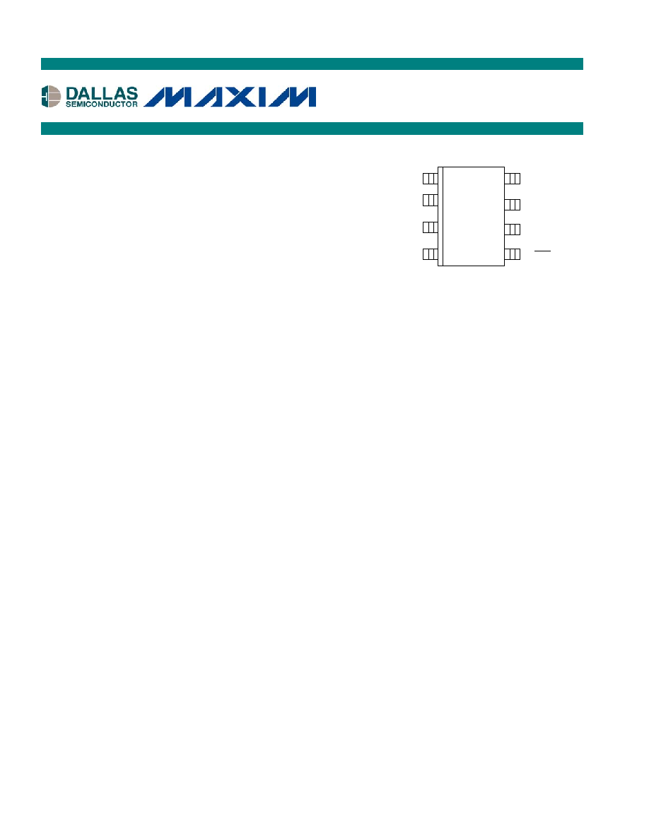
The DS1073 special is available in 8-pin DIP or SOIC packages, allowing the generation of a clock signal
easily, economically and using minimal board area.
DS1073 Special
EconOscillator/Divider
www.maxim-ic.com
DS1073Z 150-MIL SOIC
DS1073M 300-MIL DIP
OUT1
OUT0
V
CC
GND
DNC
DNC
OE
PDN
1
2
3
8
7
6
5
4

DS1073
2 of 12
BLOCK DIAGRAM Figure 1
Master
Oscillator
60-100MHz
Power
Down
Control
Divider
Divide by N
1-513
Prescaler
Divide by M
1, 2, 4
OUT0
(Optional)
(Reference)
OUT1
OE
PDN

DS1073
3 of 12
1073 SPECIAL Order Form
Use this form for DS1073 Special programmed EconOscillators . All sections must be completed.
Refer to the datasheet or contact the factory at (972) 371-6822 for assistance.
Parent Part Number:
DS1073
Customer Name: _______________________________________________________________
Customer Contact: _____________________________________________________________
Customer Address: _____________________________________________________________
_____________________________________________________________________________
Customer Phone: (Area) _____ _____ ________
Salesman: ____________________________________________________________________
Sales Representative: ___________________________________________________________
Distributor (if any): ____________________________________________________________
Package: 300mil 8-pin DIP 150mil 8-pin SOIC (circle one)
Parent Device: DS ________________ ( part will be branded with this speed)
Master Frequency: _________ MHz Standard or Special (circle one)
(60,66,80 or 100MHz)
Reference Output: Disabled
Enabled - Frequency _________
(Equals master frequency/M)
Output Frequency: _________ (Equals master frequency/MN)
Prescaler (M) : _________
Divider (N): _________
Special Instructions (Tape & Reel, etc.):
_____________________________________________________________________________
_____________________________________________________________________________
_____________________________________________________________________________
_____________________________________________________________________________
_____________________________________________________________________________
Customer Signature: _____________________________________
(acknowledges acceptance of special settings)
Fax the completed form to Louis Grantham at (972) 371-4799 (FAX).

DS1073
4 of 12
PIN DESCRIPTIONS
Output Pin (OUT1 pin): This pin is the main oscillator output.
Output Enable Function (OE pin): The DS1073 Special features a "synchronous" output enable. When
OE is at a high logic level the oscillator free runs. When this pin is taken low OUT1 is held low,
immediately if OUT1 is already low, or at the next high-to-low transition if OUT1 is high. This prevents
any possible truncation of the output pulse width when the enable is used. While the output is disabled
the master oscillator continues to run (producing an output at OUT0, if the
EN0 bit = 0) but the internal
counters (/N) are reset. This results in a constant phase relationship between OE's return to a high level
and the resulting OUT1 signal. When the enable is released OUT1 will make its first transition within
one to two clock periods of the master clock.
Power-Down (
PDN
pin):
A low logic level on this pin can be used to make the device stop oscillating
(active low) and go into a reduced power consumption state. Internal "Enabling Sequencer" circuitry
will first disable OUT in the same way as when OE is used. Next OUT0 will be disabled in a similar
fashion. Finally the oscillator circuitry will be disabled. In this mode both outputs will go into a high
impedance state. The power consumption in the power-down state is much less than if OE is used
because the internal oscillator is completely powered down. Consequently the device will take
considerably longer to recover (i.e., achieve stable oscillation) from a power-down condition than if the
OE is used.
Reference Output (OUT0 pin):
A reference output, OUT0, is also available from the output of the
prescaler. OUT0 is unaffected by the OE pin, but is disabled in a glitchless fashion if the device is
powered down. If this output is not required it can be permanently disabled and there will be a
corresponding reduction in overall power consumption. The availability of this output and its frequency
are specified on the special order form.
DNC:
Do not connect.
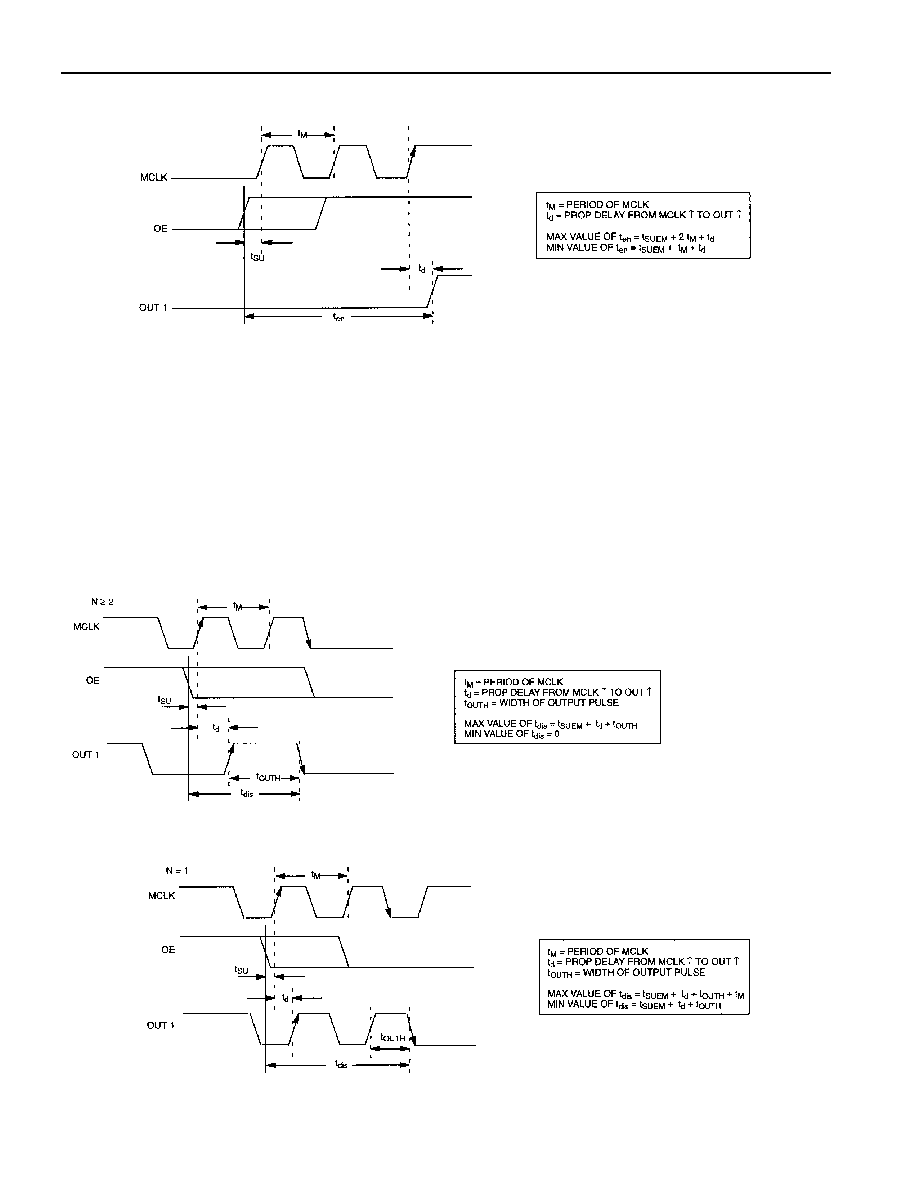
OPERATION OF OUTPUT ENABLE
Since the output enable and internal master oscillator are asynchronous there is the possibility of timing
difficulties in the application. To minimize these difficulties the DS1073 features an "enabling
sequencer" to produce predictable results when the device is enabled and disabled. In particular the
output gating is configured so that truncated output pulses can never be produced.
ENABLE TIMING
The output enable function is produced by sampling the OE input with the output from the pre-scaler mux
(MCLK) and gating this with the output from the programmable divider. The exact behavior of the
device is therefore dependent on the setup time (t
SU
) from a transition on the OE input to the rising edge
of MCLK. If the actual setup time is less than T
SUEM
then one more complete cycle of MCLK will be
required to complete the enable or disable operation (see diagrams). This is unlikely to be of any
consequence in most applications, and then only if the value for N is small. In general, the output will
make its first positive transition between approximately one and two clock periods of MCLK after the
rising edge of OE. (Figure 2)
DS1073
5 of 12
Figure 2
Disable Timing
If OE goes low while OUT1 is high, the output will be disabled on the completion of the output pulse. If
OUT1 is low, the disabling behavior will be dependent on the setup time between the falling edge of OE
and the rising edge of MCLK. If t
SU
< T
SUEM
the result will be one additional pulse appearing on the
output before disabling occurs.
If the device is in divide-by-one mode, the disabling occurs slightly differently. In this case if t
SU
> T
SUEM
one additional output pulse will appear, if t
SU
<
T
SUEM
then two additional output pulses will appear. The
following diagrams illustrate the timing in each of these cases. (Figure 3 and 4)
Figure 3
Figure 4