 | –≠–Ľ–Ķ–ļ—ā—Ä–ĺ–Ĺ–Ĺ—č–Ļ –ļ–ĺ–ľ–Ņ–ĺ–Ĺ–Ķ–Ĺ—ā: DS1089L | –°–ļ–į—á–į—ā—Ć:  PDF PDF  ZIP ZIP |

General Description
The DS1089L is a clock generator that produces a
spread spectrum (dithered) square-wave output of fre-
quencies from 130kHz to 66.6MHz. The DS1089L is
shipped from the factory programmed at a specific fre-
quency. The DS1089L is pin-for-pin compatible with the
DS1087L, however, the DS1089L dithers at equal per-
centages above and below the center frequency. The
user still has access to the internal frequency divider,
selectable Ī1%, Ī2%, Ī4%, or Ī8% dithered output,
dithering rate, and programmable output power-
down/disable mode through an I
2
CTM-compatible pro-
gramming interface. All the device settings are stored
in nonvolatile (NV) EEPROM allowing it to operate in
stand-alone applications. The DS1089L also has
power-down and output-enable control pins for power-
sensitive applications.
Applications
Automotive Infotainment
Printers
Copiers
Computer Peripherals
POS Terminals
Cable Modems
Features
Factory-Programmed Square-Wave Generator
from 33.3MHz to 66.6MHz
Center Frequency Remains Constant Independent
of Dither Percentage
No External Timing Components Required
EMI Reduction
Variable Dither Frequency
User Programmable Down to 130kHz with Divider
(Dependent on Master Oscillator Frequency)
Ī1%, Ī2%, Ī4%, or Ī8% Selectable Dithered
Output
Glitchless Output-Enable Control
I
2
C-Compatible Serial Interface
Nonvolatile Settings
Power-Down Mode
Programmable Output Power-Down/Disable Mode
DS1089L
3.3V Center Spread-Spectrum EconOscillatorTM
______________________________________________ Maxim Integrated Products
1
Rev 0; 9/04
For pricing, delivery, and ordering information, please contact Maxim/Dallas Direct! at
1-888-629-4642, or visit Maxim's website at www.maxim-ic.com.
*See Standard Frequency Options Table.
Ordering Information
Pin Configuration and Typical Operating Circuits appear at end of data sheet.
PART
TEMP RANGE
PIN-PACKAGE
DS1089LU-yxx*
-40
įC to +85įC
8 ĶSOP (118 mil)
Add "/T" for Tape and Reel.
Custom frequencies available, contact factory.
Standard Frequency Options
PART
FREQUENCY (MHz)
SPREAD (Ī%)
DITHER FREQUENCY
DS1089LU-21G
14.7456
1
f
MOSC
/ 4096
DS1089LU-4CL
18.432
2
f
MOSC
/ 4096
DS1089LU-22F
24.576
1
f
MOSC
/ 2048
DS1089LU-23C
33.3
1
f
MOSC
/ 4096
DS1089LU-450
50.0
2
f
MOSC
/ 4096
DS1089LU-866
66.6
4
f
MOSC
/ 4096
DS1089LU-yxx
Fixed up to 66.6
1, 2, 4, or 8
f
MOSC
/ 2048 or 4096 or 8192
EconOscillator is a trademark of Dallas Semiconductor Corp.
I
2
C is a trademark of Philips Corp. Purchase of I
2
C components from Maxim Integrated Products, Inc., or one of its sublicensed
Associated Companies, conveys a license under the Philips I
2
C Patent Rights to use these components in an I
2
C system, provided
that the system conforms to the I
2
C Standard Specification as defined by Philips.
DS1089L
3.3V Center Spread-Spectrum EconOscillatorTM
2
_____________________________________________________________________
ABSOLUTE MAXIMUM RATINGS
Stresses beyond those listed under "Absolute Maximum Ratings" may cause permanent damage to the device. These are stress ratings only, and functional
operation of the device at these or any other conditions beyond those indicated in the operational sections of the specifications is not implied. Exposure to
absolute maximum rating conditions for extended periods may affect device reliability.
Voltage on V
CC
Relative to Ground.......................-0.5V to +6.0V
Voltage on SPRD, PDN, OE, SDA,
SCL Relative to Ground* ........................-0.5V to (V
CC
+ 0.5V)
Operating Temperature Range ...........................-40įC to +85įC
Programming Temperature Range .........................0įC to +70įC
Storage Temperature Range .............................-55įC to +125įC
Soldering Temperature...................See IPC/JEDEC J-STD-020A
PARAMETER
SYMBOL
CONDITION
MIN
TYP
MAX
UNITS
Supply Voltage
V
CC
(Note 1)
2.7
3.3
3.6
V
High-Level Input Voltage
(SDA, SCL, SPRD, PDN, OE)
V
IH
0.7 x V
CC
V
CC
+
0.3
V
Low-Level Input Voltage
(SDA, SCL, SPRD, PDN, OE)
V
IL
-0.3
0.3 x
V
CC
V
*This voltage must not exceed 6.0V.
RECOMMENDED OPERATING CONDITIONS
(T
A
= -40įC to +85įC)
PARAMETER
SYMBOL
CONDITION
MIN
TYP
MAX
UNITS
High-Level Output Voltage (OUT)
V
OH
I
OH
= -4mA, V
CC
= min
2.4
V
Low-Level Output Voltage (OUT)
V
OL
I
OL
= 4mA
0.4
V
V
OL1
3mA sink current
0.4
Low-Level Output Voltage (SDA)
V
OL2
6mA sink current
0.6
V
High-Level Input Current
I
IH
V
IH
= V
CC
1
ĶA
Low-Level Input Current
I
IL
V
IL
= 0V
-1
ĶA
Supply Current (Active)
I
CC
C
L
= 15pF, f
OUT
= f
MOSCmax
12
mA
Standby Current (Power-Down)
I
CCQ
Power-down mode
10
ĶA
DC ELECTRICAL CHARACTERISTICS
(V
CC
= +2.7V to +3.6V, T
A
= -40įC to +85įC)

DS1089L
3.3V Center Spread-Spectrum EconOscillatorTM
_____________________________________________________________________
3
PARAMETER
SYMBOL
CONDITION
MIN
TYP
MAX
UNITS
Internal Master Oscillator
Frequency
f
MOSC
33.3
66.6
MHz
Master Oscillator Frequency
Tolerance
V
CC
= 3.3V,
T
A
= +25įC (Note 2)
-0. 5
+0. 5
%
Voltage Frequency
Variation
T
A
= +25įC (Note 3)
-0.75
+0.75
%
T
A
= 0įC to +85įC
-0.75
+0.75
Temperature Frequency Variation
(Note 4)
V
CC
= 3.3V,
f
OUT
= f
MOSCmax
T
A
= -40įC to 0įC
-2.00
+0.75
%
J3 = J2 = GND
Ī1
J3 = GND, J2 = V
CC
Ī2
J3 = V
CC
, J2 = GND
Ī4
Dither Frequency Range
(Note 5)
J3 = J2 = V
CC
Ī8
%
J1 = GND, J0 = V
CC
f
MOSC
/ 2048
J1 = V
CC
, J0 = GND
f
MOSC
/ 4096
Dither Frequency
(Note 5)
f
MOD
J1 = J0 = V
CC
f
MOSC
/ 8192
Hz
MASTER OSCILLATOR CHARACTERISTICS
(V
CC
= +2.7V to +3.6V, T
A
= -40įC to +85įC)
PARAMETER
SYMBOL
CONDITION
MIN
TYP
MAX
UNITS
Frequency Stable After
PRESCALER Change
1
Period
Power-Up Time
t
POR
+
t
STAB
(Note 6)
40
200
Ķs
Enable of OUT After Exiting
Power-Down Mode
t
STAB
(Note 6)
512
clock
cycles
OUT Disabled After Entering
Power-Down Mode
t
PDN
7
Ķs
Load Capacitance
C
L
15
50
pF
Prescaler = 1
45
55
Output Duty Cycle (f
OUT
)
Prescaler > 1
50
%
AC ELECTRICAL CHARACTERISTICS
(V
CC
= +2.7V to +3.6V, T
A
= -40įC to +85įC)
f
f
MOSC
MOSC
f
f
MOSC
f
f
MOSC
DS1089L
3.3V Center Spread-Spectrum EconOscillatorTM
4
_____________________________________________________________________
Note 1: All voltages are referenced to ground.
Note 2: This is the absolute accuracy of the master oscillator frequency at the default settings with spread disabled.
Note 3: This is the change that is observed in master oscillator frequency with changes in voltage at T
A
= +25įC.
Note 4: This is the change that is observed in master oscillator frequency with changes in temperature at V
CC
= 3.3V.
Note 5: The dither deviation of the master oscillator frequency is biderectional and results in an output frequency centered at the
undithered frequency.
Note 6: This indicates the time elapsed between power-up and the output becoming active. An on-chip delay is intentionally intro-
duced to allow the oscillator to stabilize. t
STAB
is equivalent to 512 master clock cycles and will depend on the pro-
grammed master oscillator frequency.
Note 7: Timing shown is for fast-mode (400kHz) operation. This device is also backward compatible with I
2
C standard-mode timing.
Note 8: CB--total capacitance of one bus line in picofarads.
Note 9: EEPROM write time applies to all the EEPROM memory and SRAM shadowed EEPROM memory when WC = 0.
The EEPROM write time begins after a stop condition occurs.
PARAMETER
SYMBOL
CONDITIONS
MIN
TYP
MAX
UNITS
SCL Clock Frequency
f
SCL
(Note 7)
0
400
kHz
Bus Free Time Between Stop and
Start Conditions
t
BUF
1.3
Ķs
Hold Time (Repeated) Start
Condition
t
HD:STA
0.6
Ķs
Low Period of SCL
t
LOW
1.3
Ķs
High Period of SCL
t
HIGH
0.6
Ķs
Data Hold Time
t
HD:DAT
0
0.9
Ķs
Data Setup Time
t
SU:DAT
100
ns
Start Setup Time
t
SU:STA
0.6
Ķs
SDA and SCL Rise Time
t
R
(Note 8)
20 + 0.1C
B
300
ns
SDA and SCL Fall Time
t
F
(Note 8)
20 + 0.1C
B
300
ns
Stop Setup Time
t
SU:STO
0.6
Ķs
SDA and SCL Capacitive
Loading
C
B
(Note 8)
400
pF
EEPROM Write Time
t
WR
(Note 9)
10
20
ms
AC ELECTRICAL CHARACTERISTICS--I
2
C INTERFACE
(V
CC
= +2.7V to +3.6V, T
A
= -40įC to +85įC, unless otherwise noted. Timing referenced to V
IL(MAX)
and V
IH(MIN)
.)
PARAMETER
SYMBOL
CONDITION
MIN
TYP
MAX
UNITS
Writes
+70įC
10,000
NONVOLATILE MEMORY CHARACTERISTICS
(V
CC
= +2.7V to +3.6V)
DS1089L
3.3V Center Spread-Spectrum EconOscillatorTM
_____________________________________________________________________
5
0
2
6
4
8
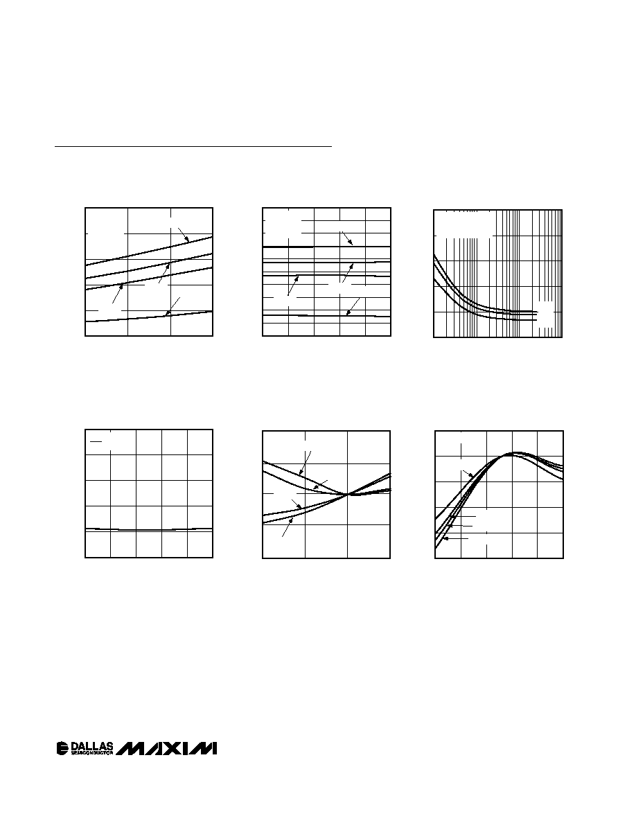
10
ACTIVE SUPPLY CURRENT
vs. SUPPLY VOLTAGE
DS 1089L toc01
SUPPLY VOLTAGE (V)
SUPPLY CURRENT (mA)
2.7
3.0
3.3
3.6
66MHz
50MHz
130kHz
33MHz
T
A
= +25įC,
OUTPUT
UNLOADED
0
3
2
1
4
5
6
7
8
9
10
-40
10
-15
35
60
85
ACTIVE SUPPLY CURRENT
vs. TEMPERATURE
DS 1089L toc02
TEMPERATURE (įC)
SUPPLY CURRENT (mA)
66MHz
50MHz
130kHz
33MHz
T
A
= +25įC,
OUTPUT
UNLOADED
0
1
1000
100
10
SUPPLY CURRENT
vs. PRESCALER
10
4
2
8
6
DS 1089L toc03
PRESCALE DIVIDER (DECIMAL)
SUPPLY CURRENT (mA)
3.6V
3.3V
2.7V
T
A
= +25įC,
f
MOSC
= 50MHz,
OUTPUT UNLOADED
0
1
3
2
4
5
-40
10
-15
35
60
85
SHUTDOWN SUPPLY CURRENT
vs. TEMPERATURE
DS 1089L toc04
TEMPERATURE (įC)
SUPPLY CURRENT (
Ķ
A)
V
CC
= 3.3V,
PDN = GND
-0.50
-0.25
0
0.25
0.50
2.7
3.0
3.3
3.6
FREQUENCY % CHANGE
vs. SUPPLY VOLTAGE
DS 1089L toc05
SUPPLY VOLTAGE (V)
FREQUENCY CHANGE (%)
66MHz
50MHz
130kHz
33MHz
T
A
= +25įC
-0.8
-0.6
-0.2
-0.4
0
0.2
-40
10
-15
35
60
85
FREQUENCY % CHANGE
vs. TEMPERATURE
DS 1089L toc06
TEMPERATURE (įC)
FREQUENCY CHANGE (%)
66MHz
50MHz
130kHz
33MHz
V
CC
= 3.3V
Typical Operating Characteristics
(V
CC
= 3.3V, T
A
= +25įC, unless otherwise noted.)