 | –≠–ª–µ–∫—Ç—Ä–æ–Ω–Ω—ã–π –∫–æ–º–ø–æ–Ω–µ–Ω—Ç: DS1220AB | –°–∫–∞—á–∞—Ç—å:  PDF PDF  ZIP ZIP |
1 of 9
103002
FEATURES
ß 10 years minimum data retention in the
absence of external power
ß Data is automatically protected during power
loss
ß Directly replaces 2k x 8 volatile static RAM
or EEPROM
ß Unlimited write cycles
ß Low-power CMOS
ß JEDEC standard 24-pin DIP package
ß Read and write access times as fast as 100 ns
ß Lithium energy source is electrically
disconnected to retain freshness until power
is applied for the first time
ß Full ±10% V
CC
operating range (DS1220AD)
ß Optional ±5% V
CC
operating range
(DS1220AB)
ß Optional industrial temperature range of
-40∞C to +85∞C, designated IND
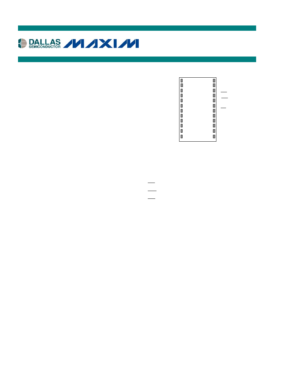
PIN ASSIGNMENT
24-Pin ENCAPSULATED PACKAGE
720-mil EXTENDED
PIN DESCRIPTION
A0-A10 -
Address
Inputs
DQ0-DQ7
- Data In/Data Out
CE
- Chip Enable
WE
- Write Enable
OE
- Output Enable
V
CC
- Power (+5V)
GND -
Ground
DESCRIPTION
The DS1220AB and DS1220AD 16k Nonvolatile SRAMs are 16,384-bit, fully static, nonvolatile SRAMs
organized as 2048 words by 8 bits. Each NV SRAM has a self-contained lithium energy source and
control circuitry which constantly monitors V
CC
for an out-of-tolerance condition. When such a condition
occurs, the lithium energy source is automatically switched on and write protection is unconditionally
enabled to prevent data corruption. The NV SRAMs can be used in place of existing 2k x 8 SRAMs
directly conforming to the popular bytewide 24-pin DIP standard. The devices also match the pinout of
the 2716 EPROM and the 2816 EEPROM, allowing direct substitution while enhancing performance.
There is no limit on the number of write cycles that can be executed and no additional support circuitry is
required for microprocessor interfacing.
DS1220AB/AD
16k Nonvolatile SRAM
www.maxim-ic.com
14
VCC
WE
1
2
3
4
5
6
7
8
9
10
11
12
13
24
15
23
22
21
20
19
18
17
16
A7
A5
A3
A2
A1
A0
DQ0
DQ1
GND
DQ2
A6
A4
A8
A9
OE
A10
CE
DQ7
DQ6
DQ5
DQ3
DQ4

DS1220AB/AD
2 of 9
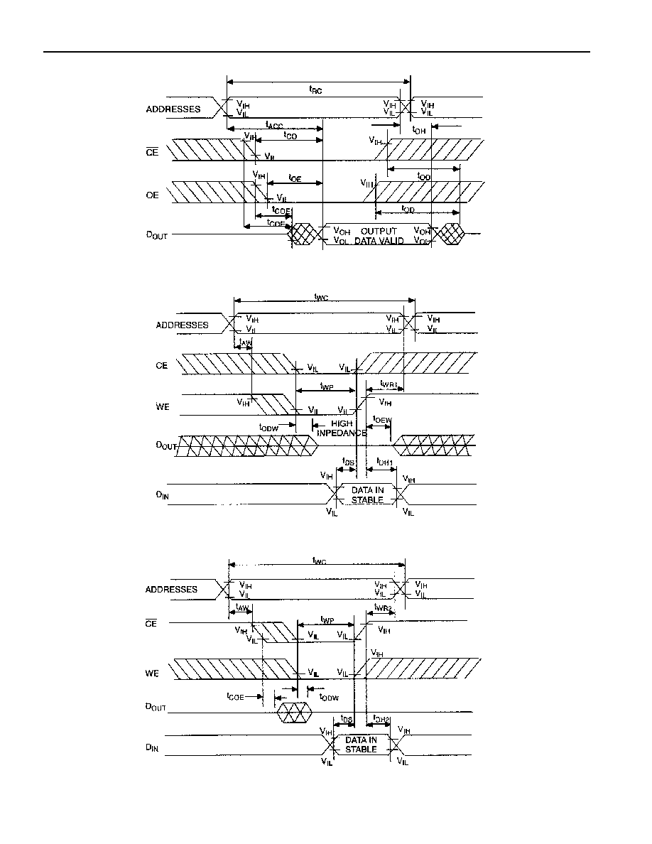
READ MODE
The DS1220AB and DS1220AD execute a read cycle whenever WE (Write Enable) is inactive (high) and
CE (Chip Enable) and OE (Output Enable) are active (low). The unique address specified by the 11
address inputs (A0-A10) defines which of the 2048 bytes of data is to be accessed. Valid data will be
available to the eight data output drivers within t
ACC
(Access Time) after the last address input signal is
stable, providing that the CE and OE access times are also satisfied. If CE and OE access times are not
satisfied, then data access must be measured from the later-occurring signal and the limiting parameter is
either t
CO
for CE or t
OE
for OE rather than address access.
WRITE MODE
The DS1220AB and DS1220AD execute a write cycle whenever the WE and CE signals are active (low)
after address inputs are stable. The latter occurring falling edge of CE or WE will determine the start of
the write cycle. The write cycle is terminated by the earlier rising edge of CE or WE . All address inputs
must be kept valid throughout the write cycle. WE must return to the high state for a minimum recovery
time (t
WR
) before another cycle can be initiated. The OE control signal should be kept inactive (high)
during write cycles to avoid bus contention. However, if the output drivers are enabled ( CE and OE
active) then WE will disable the outputs in t
ODW
from its falling edge.
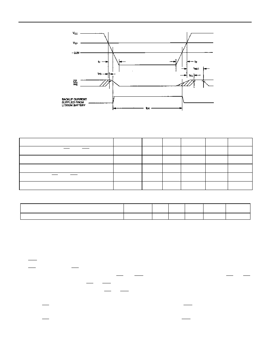
DATA RETENTION MODE
The DS1220AB provides full functional capability for V
CC
greater than 4.75 volts and write protects by
4.5V. The DS1220AD provides full functional capability for V
CC
greater than 4.5 volts and write protects
by 4.25V. Data is maintained in the absence of V
CC
without any additional support circuitry. The
nonvolatile static RAMs constantly monitor V
CC
. Should the supply voltage decay, the NV SRAMs
automatically write protect themselves, all inputs become "don't care," and all outputs become high
impedance. As V
CC
falls below approximately 3.0 volts, a power switching circuit connects the lithium
energy source to RAM to retain data. During power-up, when V
CC
rises above approximately 3.0 volts,
the power switching circuit connects external V
CC
to RAM and disconnects the lithium energy source.
Normal RAM operation can resume after V
CC
exceeds 4.75 volts for the DS1220AB and 4.5 volts for the
DS1220AD.
FRESHNESS SEAL
Each DS1220 device is shipped from Dallas Semiconductor with its lithium energy source disconnected,
guaranteeing full energy capacity. When V
CC
is first applied at a level of greater than V
TP
, the lithium
energy source is enabled for battery backup operation.
DS1220AB/AD
3 of 9
ABSOLUTE MAXIMUM RATINGS*
Voltage on Any Pin Relative to Ground
-0.3V to +7.0V
Operating Temperature
0∞C to 70∞C; -40∞C to +85∞C for IND parts
Storage Temperature
-40∞C to +70∞C; -40∞C to +85∞C for IND parts
Soldering Temperature
260∞C for 10 seconds
* This is a stress rating only and functional operation of the device at these or any other conditions
above those indicated in the operation sections of this specification is not implied. Exposure to
absolute maximum rating conditions for extended periods of time may affect reliability.
RECOMMENDED DC OPERATING CONDITIONS
(T
A
: See Note 10)
PARAMETER
SYMBOL MIN TYP MAX UNITS NOTES
DS1220AB Power Supply Voltage
V
CC
4.75
5.0
5.25
V
DS1220AD Power Supply Voltage
V
CC
4.50
5.0
5.50
V
Logic 1
V
IH
2.2
V
CC
V
Logic 0
V
IL
0.0
+0.8
V
(T
A
: See Note 10)
(V
CC
=5V
± 5% for DS1220AB)
DC ELECTRICAL CHARACTERISTICS (V
CC
=5V
± 10% for DS1220AD)
PARAMETER
SYMBOL MIN TYP MAX UNITS NOTES
Input Leakage Current
I
IL
-1.0
+1.0
mA
I/O Leakage Current
CE
≥ V
IH
£ V
CC
I
IO
-1.0
+1.0
mA
Output Current @ 2.4V
I
OH
-1.0
mA
Output Current @ 0.4V
I
OL
2.0
mA
Standby Current CE
=
2.2V
I
CCS1
5.0
10.0
mA
Standby Current CE
=
V
CC
-0.5V
I
CCS2
3.0
5.0
mA
Operating Current
(Commercial)
I
CC01
75
mA
Operating Current
(Industrial)
I
CCO1
85
mA
Write Protection Voltage
(DS1220AB)
V
TP
4.5
4.62
4.75
V
Write Protection Voltage
(DS1220AD)
V
TP
4.25
4.37
4.5
V
CAPACITANCE
(T
A
=25∞C)
PARAMETER
SYMBOL MIN TYP MAX UNITS NOTES
Input Capacitance
C
IN
5
10
pF
Input/Output Capacitance
C
I/O
5
12
pF
DS1220AB/AD
4 of 9
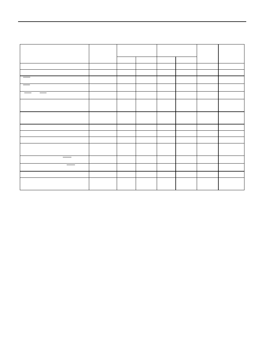
(T
A
:
See Note 10)
(V
CC
=5.0V
± 5% for DS1220AB)
AC ELECTRICAL CHARACTERISTICS (V
CC
=5.0V
± 10% for DS1220AD)
DS1220AB-100
DS1220AD-100
DS1220AB-120
DS1220AD-120
PARAMETER
SYMBOL
MIN
MAX
MIN
MAX
UNITS
NOTES
Read Cycle Time
t
RC
100
120
ns
Access Time
t
ACC
100
120
ns
OE
to Output Valid
t
OE
50
60
ns
CE
to Output Valid
t
CO
100
120
ns
OE
or
CE to Output Active
t
COE
5
5
ns
5
Output High Z from
Deselection
t
OD
35
35
ns
5
Output Hold from Address
Change
t
OH
5
5
ns
Write Cycle Time
t
WC
100
120
ns
Write Pulse Width
t
WP
75
90
ns
3
Address Setup Time
t
AW
0
0
ns
Write Recovery Time
t
WR1
t
WR2
0
10
0
10
ns
ns
12
13
Output High from WE
t
ODW
35
35
ns
5
Output Active from WE
t
OEW
5
5
ns
4
Data Setup Time
t
DS
40
50
ns
4
Data Hold Time
t
DH1
t
DH2
0
10
0
10
ns
ns
12
13
DS1220AB/AD
5 of 9
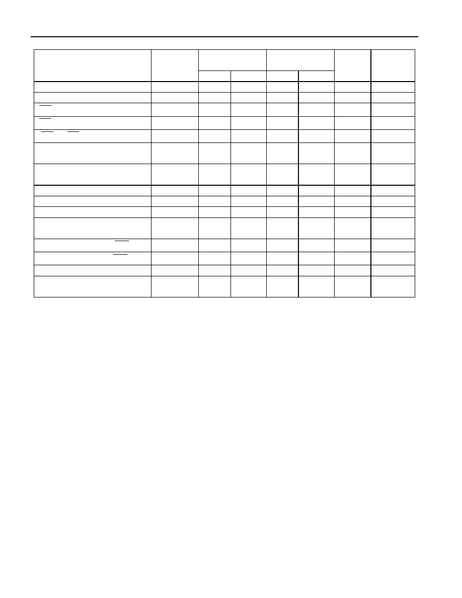
AC ELECTRICAL CHARACTERISTICS
(cont'd)
DS1220AB-150
DS1220AD-150
DS1220AB-200
DS1220AD-200
PARAMETER
SYMBOL
MIN
MAX
MIN
MAX
UNITS
NOTES
Read Cycle Time
t
RC
150
200
ns
Access Time
t
ACC
150
200
ns
OE
to Output Valid
t
OE
70
100
ns
CE
to Output Valid
t
CO
150
200
ns
OE
or
CE to Output Active
t
COE
5
5
ns
5
Output High Z from
Deselection
t
OD
35
35
ns
5
Output Hold from Address
Change
t
OH
5
5
ns
Write Cycle Time
t
WC
150
200
ns
Write Pulse Width
t
WP
100
150
ns
3
Address Setup Time
t
AW
0
0
ns
Write Recovery Time
t
WR1
t
WR2
0
10
0
10
ns
ns
12
13
Output High Z from WE
t
ODW
35
35
ns
5
Output Active from WE
t
OEW
5
5
ns
4
Data Setup Time
t
DS
60
50
ns
4
Data Hold Time
t
DH1
t
DH2
0
10
0
10
ns
ns
12
13
DS1220AB/AD
6 of 9
READ CYCLE
SEE NOTE 1
WRITE CYCLE 1
SEE NOTES 2, 3, 4, 6, 7, 8 AND 12
WRITE CYCLE 2
SEE NOTES 2, 3, 4, 6, 7, 8 AND 13
DS1220AB/AD
7 of 9
POWER-DOWN/POWER-UP CONDITION
SEE NOTE 11
POWER-DOWN/POWER-UP TIMING
(T
A
: See Note 10)
PARAMETER
SYMBOL
MIN
TYP
MAX
UNITS NOTES
V
CC
Fail Detect to
CE
and
WE
Inactive
t
PD
1.5
ms
11
V
CC
slew from V
TP
to 0V
t
F
300
ms
V
CC
slew from 0V to V
TP
t
R
300
ms
V
CC
Valid to
CE
and
WE
Inactive
t
PU
2
ms
V
CC
Valid to End of Write Protection
t
REC
125
ms
(T
A
=25∞C)
PARAMETER
SYMBOL MIN TYP MAX UNITS NOTES
Expected Data Retention Time
t
DR
10
years
9
WARNING:
Under no circumstances are negative undershoots, of any amplitude, allowed when device is in the
battery backup mode.
NOTES:
1. WE is high for a read cycle.
2. OE = V
IH
or V
IL
. If OE = V
IH
during write cycle, the output buffers remain in a high-impedance state.
3. t
WP
is specified as the logical AND of CE and WE . t
WP
is measured from the latter of CE or CE
going low to the earlier of CE or WE going high.
4. t
DS
is measured from the earlier of CE or WE going high.
5. These parameters are sampled with a 5 pF load and are not 100% tested.
6. If the CE low transition occurs simultaneously with or later than the WE low transition, the output
buffers remain in a high-impedance state during this period.
7. If the CE high transition occurs prior to or simultaneously with the WE high transition, the output
buffers remain in a high-impedance state during this period.
DS1220AB/AD
8 of 9
8. If WE is low or the WE low transition occurs prior to or simultaneously with the CE low transition,
the output buffers remain in a high-impedance state during this period.
9. Each DS1220AB and each DS1220AD has a built-in switch that disconnects the lithium source until
V
CC
is first applied by the user. The expected t
DR
is defined as accumulative time in the absence of
V
CC
starting from the time power is first applied by the user.
10. All AC and DC electrical characteristics are valid over the full operating temperature range. For
commercial products, this range is 0∞C to 70∞C. For industrial products (IND), this range is -40∞C to
+85∞C.
11. In a power down condition the voltage on any pin may not exceed the voltage on V
CC
.
12. t
WR1
, t
DH1
are measured from WE going high.
13. t
WR2
, t
DH2
are measured from CE going high.
14. DS1220 modules are recognized by Underwriters Laboratory (U.L.
“) under file E99151.
DC TEST CONDITIONS
Outputs Open
Cycle = 200ns for Operating Current
All Voltages Are Referenced to Ground
AC TEST CONDITIONS
Output Load: 100 pF + 1TTL Gate
Input Pulse Levels: 0 - 3.0V
Timing Measurement Reference Levels
Input: 1.5V
Output: 1.5V
Input Pulse Rise and Fall Times: 5ns
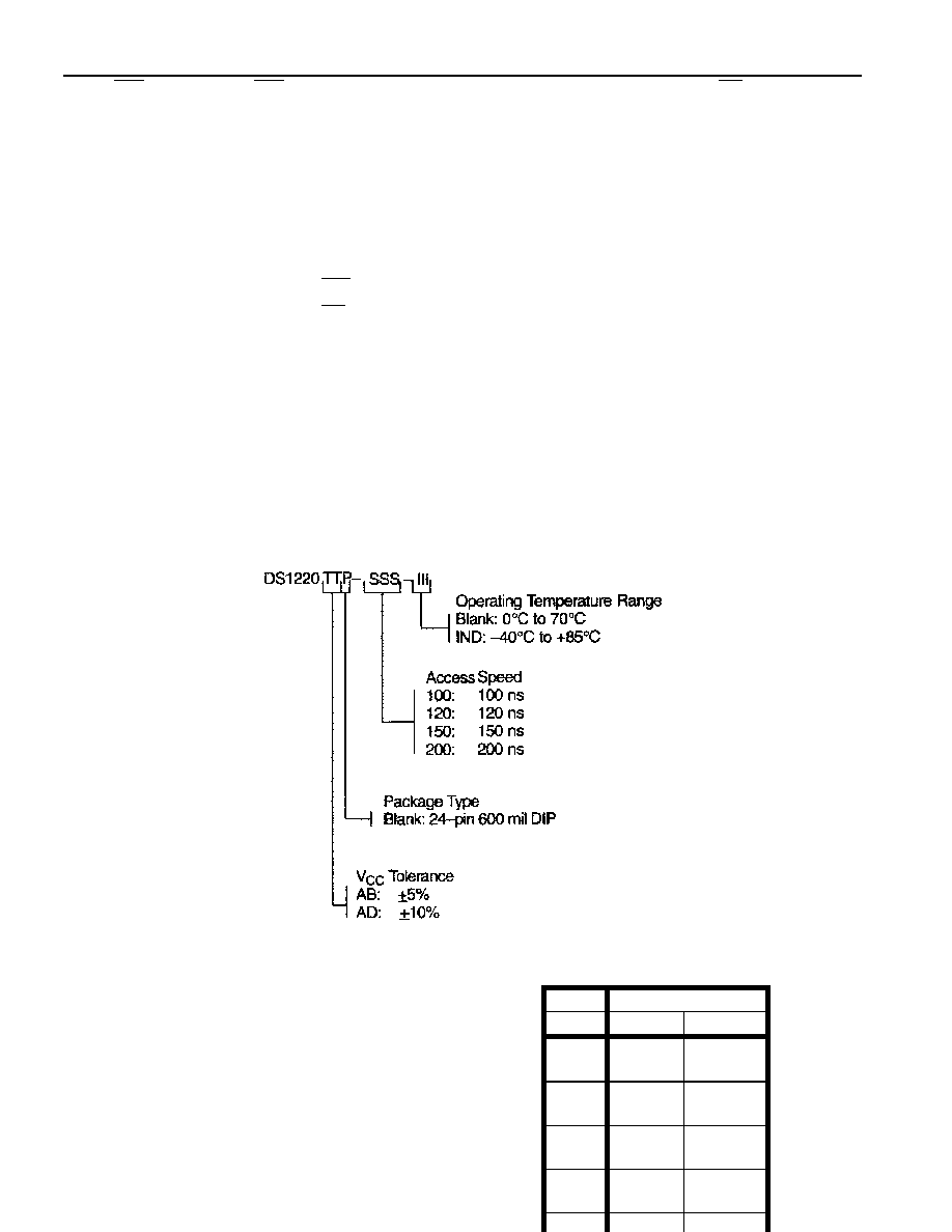
ORDERING INFORMATION
DS1220AB/AD NONVOLATILE SRAM, 24-PIN 720-MIL EXTENDED MODULE
PKG
24-PIN
DIM
MIN
MAX
A IN.
MM
1.320
33.53
1.340
34.04
B IN.
MM
0.695
17.65
0.720
18.29
C IN.
MM
0.390
9.91
0.415
10.54
D IN.
MM
0.100
2.54
0.130
3.30
E IN.
0.017
0.030
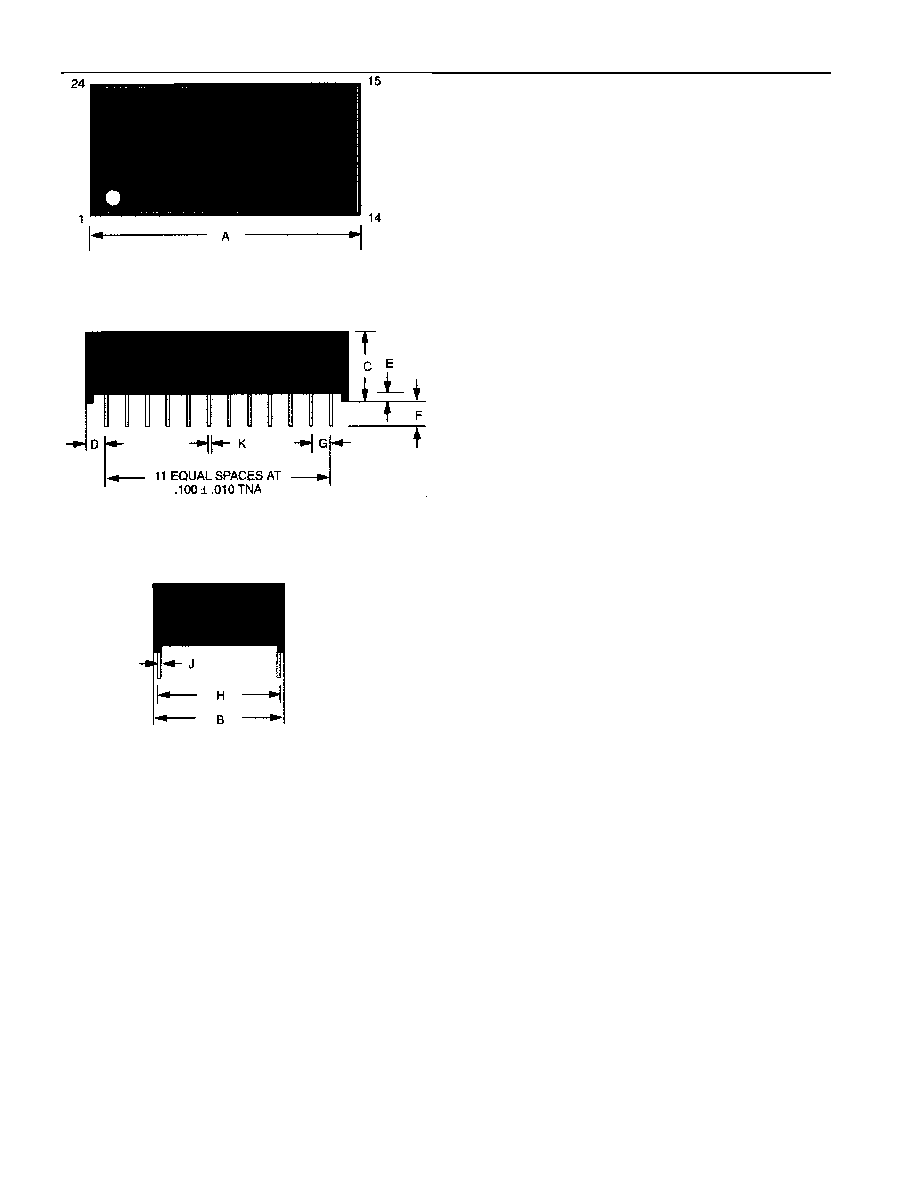
DS1220AB/AD
9 of 9