 | –≠–ª–µ–∫—Ç—Ä–æ–Ω–Ω—ã–π –∫–æ–º–ø–æ–Ω–µ–Ω—Ç: DS1722U | –°–∫–∞—á–∞—Ç—å:  PDF PDF  ZIP ZIP |
1 of 13
080602
FEATURES
ß Temperature measurements require no
external components
ß Measures temperatures from -55∞C to
+120
∞C. Fahrenheit equivalent is -67∞F to
+248
∞F
ß Thermometer accuracy is ±2.0∞C
ß Thermometer resolution is configurable from
8 to 12 bits (1.0
∞C to 0.0625∞C resolution)
ß Data is read from/written to via a Motorola
Serial Peripheral Interface (SPI) or standard
3-wire serial interface
ß Wide analog power supply range (2.65V -
5.5V)
ß Separate digital supply allows for 1.8V logic
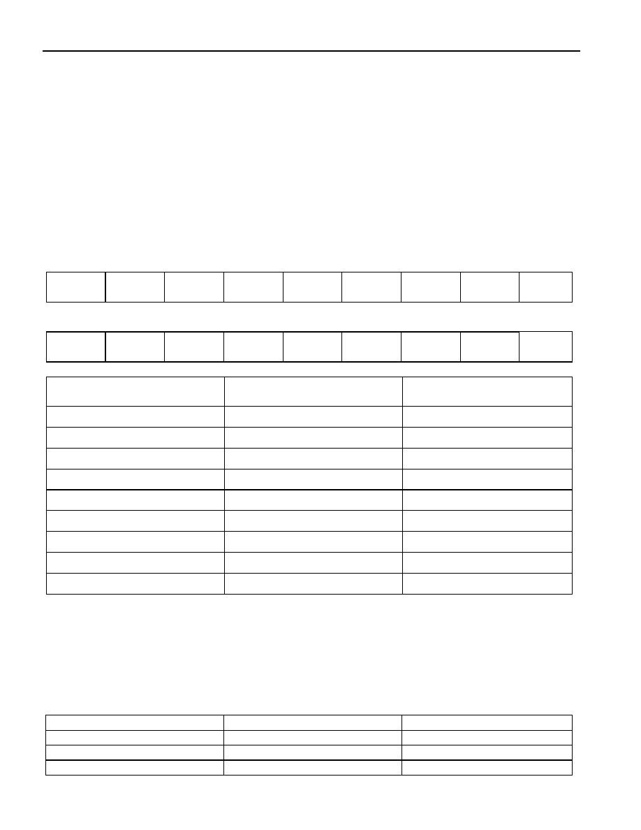
ß Available in an 8-pin SOIC (150 mil), 8-pin
uSOP, and flip chip package
PIN ASSIGNMENT
PIN DESCRIPTION
SERMODE
- Serial Interface Mode
CE
- Chip Enable
SCLK
- Serial Clock
GND -
Ground
V
DDA
- Analog Supply Voltage
SDO
- Serial Data Out
SDI
- Serial Data In
V
DDD
- Digital Supply Voltage
DESCRIPTION
The DS1722 Digital Thermometer and Thermostat with SPI/3-Wire Interface provides temperature
readings which indicate the temperature of the device. No additional components are required; the device
is truly a temperature-to-digital converter. Temperature readings are communicated from the DS1722
over a Motorola SPI interface or a standard 3-wire serial interface. The choice of interface standard is
selectable by the user.
For applications that require greater temperature resolution, the user can adjust the readout resolution
from 8 to 12 bits. This is particularly useful in applications where thermal runaway conditions must be
detected quickly.
For application flexibility, the DS1722 features a wide analog supply rail of 2.65V - 5.5V. A separate
digital supply allows a range of 1.8V to 5.5V.
The DS1722 is available in an 8-pin SOIC (150-mil), 8-pin uSOP, and flip chip package.
Applications for the DS1722 include personal computers/servers/workstations, cellular telephones, office
equipment, or any thermally-sensitive system.
DS1722
Digital Thermometer with
SPI/3-Wire Interface
PRELIMINARY
www.maxim-ic.com
V
DDD
CE
SCLK
GND
V
DDA
2
3
4
8
7
6
5
1
DS1722S
8-Pin SOIC (150-mil)
SERMODE
SDI
SDO
1 8
2 7
3 6
4 5
*
DS1722U
8-PIN µ-SOP
V
DDA
SERMODE
SDI
SDO
V
DDD
CE
SCLK
GND

DS1722
2 of 13
DETAILED PIN DESCRIPTION
Table 1
SOIC
SYMBOL
DESCRIPTION
PIN 1
V
DDD
Digital Supply Voltage 1.8V-5.5V. Defines the top rails for the digital
inputs and outputs.
PIN 2
CE
Chip Enable Must be asserted high for communication to take place for
either the SPI or 3-wire interface.
PIN 3
SCLK
Serial Clock Input Used to synchronize data movement on the serial
interface for either the SPI or 3-wire interface.
PIN 4
GND
Ground pin.
PIN 5
SDO
Serial Data Output When SPI communication is selected, the SDO pin is
the serial data output for the SPI bus. When 3-wire communication is
selected, this pin must be tied to the SDI pin (the SDI and SDO pins function
as a single I/O pin when tied together.)
PIN 6
SDI
Serial Data Input When SPI communication is selected, the SDI pin is the
serial data input for the SPI bus. When 3-wire communication is selected,
this pin must be tied to the SDO pin (the SDI and SDO pins function as a
single I/O pin when tied together.)
PIN 7
SERMODE
Serial Interface Mode Input This pin selects which interface standard will
be used: SPI when connected to V
CC
; standard 3-wire when connected to
GND.
PIN 8
V
DDA
Analog Supply Voltage 2.65V ≠ 5.5V input power pin.
OVERVIEW
A block diagram of the DS1722 is shown in Figure 1. The DS1722 consists of four major components:
1. Precision temperature sensor
2. Analog-to-digital converter
3. SPI/3-wire interface electronics
4. Data registers
The factory-calibrated temperature sensor requires no external components. The DS1722 is in a power-
conserving shutdown state upon power-up. After power-up, the user may alter the configuration register
to place the device in a continuous temperature conversion mode or in a one-shot conversion mode. In
the continuous conversion mode, the DS1722 continuously converts the temperature and stores the result
in the temperature register. As conversions are performed in the background, reading the temperature
register does not affect the conversion in progress. In the one-shot temperature conversion mode, the
DS1722 will perform one temperature conversion, store the result in the temperature register, and then
return to the shutdown state. This conversion mode is ideal for power sensitive applications. More
information on the configuration register is contained in the "OPERATION-Programming" section.
The temperature conversion results will have a default resolution of 9 bits. In applications where small
incremental temperature changes are critical, the user can change the conversion resolution from 9 bits to
8, 10, 11, or 12. This is accomplished by programming the configuration register. Each additional bit of
resolution approximately doubles the conversion time.

DS1722
3 of 13
The DS1722 can communicate using either a Motorola Serial Peripheral Interface (SPI) or standard 3-
wire interface. The user can select either communication standard through the SERMODE pin, tying it to
V
DDD
for SPI and to ground for 3-wire.
The device contains both an analog supply voltage and a digital supply voltage (V
DDA
and V
DDD
,
respectively). The analog supply powers the device for operation while the digital supply provides the
top rails for the digital inputs and outputs. The DS1722 was designed to be 1.8V Logic-Ready.
DS1722 FUNCTIONAL BLOCK DIAGRAM
Figure 1
OPERATION-Measuring Temperature
The core of DS1722 functionality is its direct-to-digital temperature sensor. The DS1722 measures
temperature through the use of an on-chip temperature measurement technique with an operating range
from -55
∞ to +120∞C. The device powers up in a power-conserving shutdown mode. After power-up, the
DS1722 may be placed in a continuous conversion mode or in a one-shot conversion mode. In the
continuous conversion mode, the device continuously computes the temperature and stores the most
recent result in the temperature register at addresses 01h (LSB) and 02h (MSB). In the one-shot
conversion mode, the DS1722 performs one temperature conversion and then returns to the shutdown
mode, storing temperature in the temperature register. Details on how to change the setting after power-
up are contained in the "OPERATION-Programming" section.
DS1722
4 of 13
The resolution of the temperature conversion is configurable (8, 9, 10, 11, or 12 bits), with 9-bit readings
the default state. This equates to a temperature resolution of 1.0
∞C, 0.5∞C, 0.25∞C, 0.125∞C, or 0.0625∞C.
Following each conversion, thermal data is stored in the thermometer register in two's complement
format; the information can be retrieved over the SPI or 3-wire interface with the address set to the
temperature register, 01h (LSB) and then 02h (MSB). Table 2 describes the exact relationship of output
data to measured temperature. The table assumes the DS1722 is configured for 12-bit resolution; if the
device is configured in a lower resolution mode, those bits will contain 0s. The data is transmitted
serially over the digital interface, MSb first for SPI communication and LSb first for 3-wire
communication. The MSb of the temperature register contains the "sign" (S) bit, denoting whether the
temperature is positive or negative. For Fahrenheit usage, a lookup table or conversion routine must be
used.
Temperature/Data Relationships
Table 2
Address
Location
S
2
6
2
5
2
4
2
3
2
2
2
1
2
0
02h
MSb
(unit =
∞C)
LSb
2
-1
2
-2
2
-3
2
-4
0
0
0
0
01h
TEMPERATURE
DIGITAL OUTPUT
(BINARY)
DIGITAL OUTPUT
(HEX)
+120
∞C
0111 1000 0000 0000
7800h
+25.0625
∞C
0001 1001 0001 0000
1910h
+10.125
∞C
0000 1010 0010 0000
0A20h
+0.5
∞C
0000 0000 1000 0000
0080h
0
∞C
0000 0000 0000 0000
0000h
-0.5
∞C
1111 1111 1000 0000
FF80h
-10.125
∞C
1111 0101 1110 0000
F5E0h
-25.0625
∞C
1110 0110 1111 0000
E6F0h
-55
∞C
1100 1001 0000 0000
C900h
OPERATION-Programming
The area of interest in programming the DS1722 is the Configuration register. All programming is done
via the SPI or 3-wire communication interface by selecting the appropriate address of the desired register
location. Table 3 illustrates the addresses for the two registers (configuration and temperature) of the
DS1722.
Register Address Structure
Table 3
Read Address
Write Address
Active Register
00h
80h
Configuration
01h
No access
Temperature LSB
02h
No access
Temperature MSB
DS1722
5 of 13
CONFIGURATION REGISTER PROGRAMMING
The configuration register is accessed in the DS1722 with the 00h address for reads and the 80h address
for writes. Data is read from or written to the configuration register MSb first for SPI communication and
LSb first for 3-wire communication. The format of the register is illustrated in Figure 2. The effect each
bit has on DS1722 functionality is described below along with the power-up state of the bit. The entire
register is volatile, and thus it will power-up in the default state.
CONFIGURATION/STATUS REGISTER
Figure 2
1
1
1
1SHOT
R2
R1
R0
SD
MSb
LSb
1SHOT = One-shot temperature conversion bit. If the SD bit is "1", (continuous temperature
conversions are not taking place), a "1" written to the 1SHOT bit will cause the DS1722 to perform one
temperature conversion and store the results in the temperature register at addresses 01h (LSB) and 02h
(MSB). The bit will clear itself to "0" upon completion of the temperature conversion. The user has
read/write access to the 1SHOT bit, although writes to this bit will be ignored if the SD bit is a "0",
(continuous conversion mode). The power-up default of the one-shot bit is "0".
R0, R1, R2 = Thermometer resolution bits. Table 4 below defines the resolution of the digital
thermometer, based on the settings of these 3 bits. There is a direct tradeoff between resolution and
conversion time, as depicted in the AC Electrical Characteristics. The user has read/write access to the
R2, R1 and R0 bits and the power-up default state is R2="0", R1="0", and R0="1" (9-bit conversions).
THERMOMETER RESOLUTION CONFIGURATION Table 4
R2
R1
R0
Thermometer Resolution
Max Conversion Time
0
0
0
8-bit
0.075s
0
0
1
9-bit
0.15s
0
1
0
10-bit
0.3s
0
1
1
11-bit
0.6s
1
x
x
12-bit
1.2s
x=Don't care.
SD = Shutdown bit. If SD is "0", the DS1722 will continuously perform temperature conversions and
store the last completed result in the temperature register. If SD is changed to a "1", the conversion in
progress will be completed and stored and then the device will revert to a low-power shutdown mode.
The communication port remains active. The user has read/write access to the SD bit and the power-up
default is "1" (shutdown mode).
SERIAL INTERFACE
The DS1722 offers the flexibility to choose between two serial interface modes. The DS1722 can
communicate with the SPI interface or with a standard 3-wire interface. The interface method used is
determined by the SERMODE pin. When this pin is connected to V
DDD
SPI communication is selected.
When this pin is connected to ground, standard 3-wire communication is selected.
SERIAL PERIPHERAL INTERFACE (SPI)
The serial peripheral interface (SPI) is a synchronous bus for address and data transfer. The SPI mode of
serial communication is selected by tying the SERMODE pin to V
DDD
. Four pins are used for the SPI.
The four pins are the SDO (Serial Data Out), SDI (Serial Data In), CE (Chip Enable), and SCLK (Serial
Clock). The DS1722 is the slave device in an SPI application, with the microcontroller being the master.
DS1722
6 of 13
The SDI and SDO pins are the serial data input and output pins for the DS1722, respectively. The CE
input is used to initiate and terminate a data transfer. The SCLK pin is used to synchronize data
movement between the master (microcontroller) and the slave (DS1722) devices.
The shift clock (SCLK), which is generated by the microcontroller, is active only when CE is high and
during address and data transfer to any device on the SPI bus. The inactive clock polarity is
programmable in some microcontrollers. The DS1722 offers an important feature in that the level of the
inactive clock is determined by sampling SCLK when CE becomes active. Therefore, either SCLK
polarity can be accommodated. Input data (SDI) is latched on the internal strobe edge and output data
(SDO) is shifted out on the shift edge (See Table 5 and Figure 3). There is one clock for each bit
transferred. Address and data bits are transferred in groups of eight, MSB first.
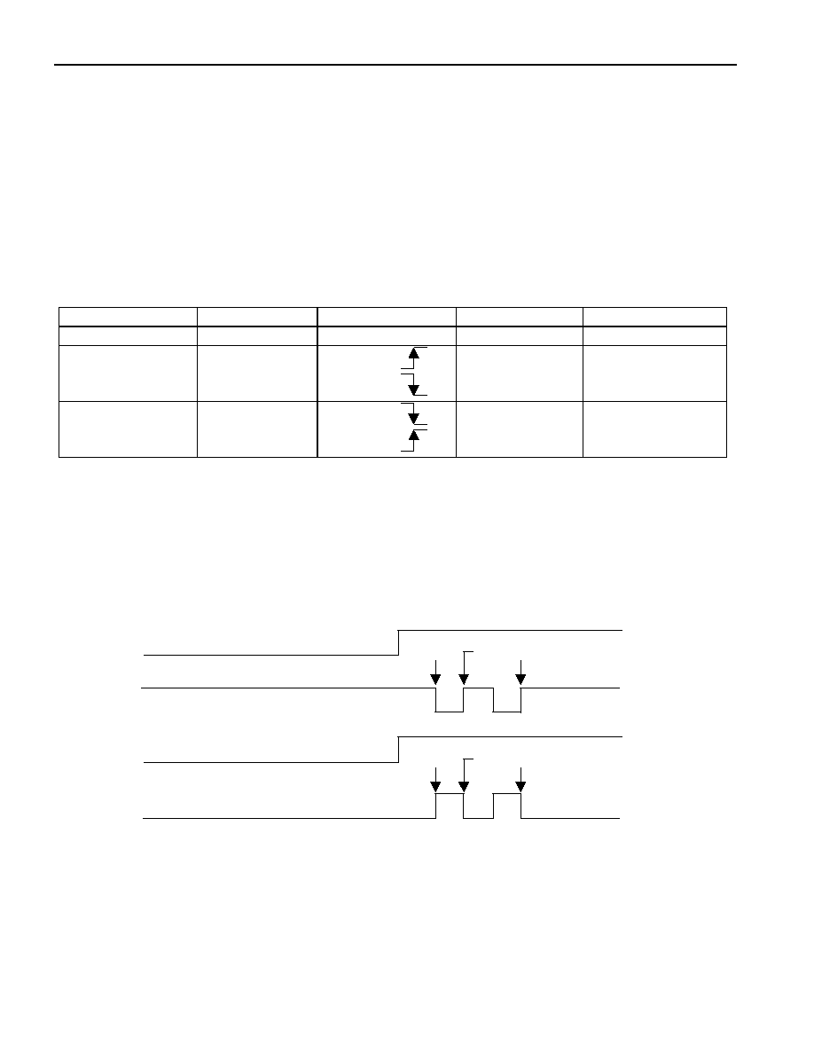
FUNCTION TABLE
Table 5
MODE
CE
SCLK
SDI
SDO
Disable Reset
L
Input Disabled
Input Disabled
High Z
Write
H
CPOL=1*
CPOL=0
Data Bit Latch
High Z
Read
H
CPOL=1
CPOL=0
X
Next data bit
shift**
*CPOL is the "Clock Polarity" bit that is set in the control register of the microcontroller.
** SDO remains at High Z until eight bits of data are ready to be shifted out during a read.
NOTE:
CPHA bit polarity must be set to "1".
SERIAL CLOCK AS A FUNCTION OF MICROCONTROLLER CLOCK
POLARITY (CPOL) Figure 3
CPOL=1
CPOL=0
NOTE:
CPOL is a bit that is set in the microcontroller's Control Register.
CE
SCLK
CE
SCLK
INTERNAL
STROBE
SHIFT
INTERNAL
STROBE
SHIFT
DS1722
7 of 13
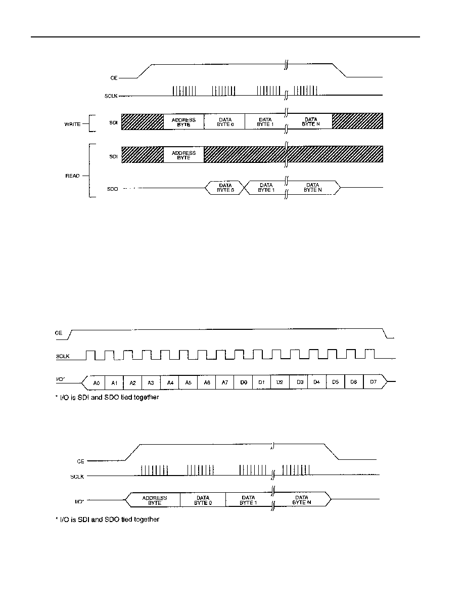
ADDRESS AND DATA BYTES
Address and data bytes are shifted MSB first into the serial data input (SDI) and out of the serial data
output (SDO). Any transfer requires the address of the byte to specify a write or a read, followed by one
or more bytes of data. Data is transferred out of the SDO for a read operation and into the SDI for a write
operation.
SPI SINGLE BYTE WRITE
Figure 4
The address byte is always the first byte entered after CE is driven high. The most significant bit (A7) of
this byte determines if a read or write will take place. If A7 is "0", one or more read cycles will occur. If
A7 is "1", one or more write cycles will occur.
Data transfers can occur 1 byte at a time in multiple-byte burst mode. After CE is driven high an address
is written to the DS1722. After the address, one or more data bytes can be written or read. For a single-
byte transfer, 1 byte is read or written and then CE is driven low (see Figures 4 and 5). For a multiple-
byte transfer, however, multiple bytes can be read or written to the DS1722 after the address has been
written (see Figure 6). A single-byte burst read/write will sequentially point through the memory map
and will loop from 02h/82h to 00h/80h.
SPI SINGLE-BYTE READ Figure 5
DS1722
8 of 13
SPI MULTIPLE BYTE BURST TRANSFER
Figure 6
3-WIRE SERIAL DATA BUS
The 3-wire communication mode operates similar to the SPI mode. However, in 3-wire mode, there is
one bi-directional I/O instead of separate data in and data out signals. The 3-wire consists of the I/O (SDI
and SDO pins tied together), CE, and SCLK pins. In 3-wire mode, each byte is shifted in LSB first
unlike SPI mode where each byte is shifted in MSB first. As is the case with the SPI mode, an address
byte is written to the device followed by a single data byte or multiple data bytes. Figure 7 illustrates a
read and write cycle. Figure 8 illustrates a multiple byte burst transfer. In 3-wire mode, data is input on
the rising edge of SCLK and output on the falling edge of SCLK.
3-WIRE SINGLE BYTE TRANSFER
Figure 7
3-WIRE MULTIPLE BYTE BURST TRANSFER Figure 8

DS1722
9 of 13
ABSOLUTE MAXIMUM RATINGS*
Voltage on V
DD
, Relative to Ground
-0.3V to +6.0V
Voltage on any other pin, Relative to Ground
-0.3V to +6.0V
Operating Temperature
-55
∞C to +125∞C
Storage Temperature
-55
∞C to +125∞C
Soldering Temperature
260∞C for 10 seconds
* This is a stress rating only and functional operation of the device at these or any other conditions above
those indicated in the operation sections of this specification is not implied. Exposure to absolute
maximum rating conditions for extended periods of time may affect reliability.
The Dallas Semiconductor DS1722 is built to the highest quality standards and manufactured for long
term reliability. All Dallas Semiconductor devices are made using the same quality materials and
manufacturing methods. However, the DS1722 is not exposed to environmental stresses, such as burn-in,
that some industrial applications require. For specific reliability information on this product, please
contact the factory in Dallas at (972) 371-4448.
RECOMMENDED DC OPERATING CONDITIONS
(-55∞C to +120∞C, 2.65V
£ V
DDA
£5.5V)
PARAMETER
SYMBOL
CONDITION
MIN TYP MAX UNITS NOTES
Analog Supply Voltage
V
DDA
2.65
5.5
V
1
Digital Supply Voltage
V
DDD
1.8
5.5
V
1
DC ELECTRICAL CHARACTERISTICS (-55
∞C to +120∞C, 2.65V £ V
DDA
£ 5.5V)
PARAMETER
SYMBOL
CONDITION
MIN TYP MAX UNITS NOTES
Input Logic High
V
IH
0.7 x
V
DDD
V
1
Input Logic Low
V
IL
0.2 x
V
DDD
V
1
Logic 0 Output
V
OL
0.2 x
V
DDD
V
2
Logic 1 Output
V
OH
0.7 x
V
DDD
V
3
Input Resistance
R
I
CE to GND
SDI, SDO,
SCLK to V
DDD
1
1
M
W
M
W
Active Current
I
CC
.5
mA
4
Shutdown Current
I
CC
2.65V
£ V
DDA
£ 3.3V
3.3V
£V
DDA
£5.5V
0.5
1.0
µ
A
µ
A

DS1722
10 of 13
ELECTRICAL CHARACTERISTICS: DIGITAL THERMOMETER
(-55
∞C to +120∞C, 2.65V £ V
DDA
£ 5.5V)
PARAMETER
SYMBOL
CONDITION
MIN
TYP MAX UNITS NOTES
-40
∞C to +85∞C
±2.0
Thermometer Error
T
ERR
-55
∞C to +120∞C
±3.0
∞C
8, 9
Resolution
8
12
bits
8-bit conversions
67.5
75
9-bit conversions
125
150
10-bit conversions
250
300
11-bit conversions
500
600
Conversion Time
t
CONVT
12-bit conversions
1000
1200
ms
AC ELECTRICAL CHARACTERISTICS: 3-WIRE INTERFACE
(-55
∞C to +120∞C, 2.65V £ V
DD
£ 5.5V)
PARAMETER
SYMBOL
CONDITION
MIN TYP MAX UNITS NOTES
Data to SCLK Setup
t
DC
35
ns
5, 6
SCLK to Data Hold
t
CDH
35
ns
5, 6
SCLK to Data Valid
t
CDD
80
ns
5, 6, 7
SCLK Low Time
t
CL
100
ns
6
SCLK High Time
t
CH
100
ns
6
SCLK Frequency
t
CLK
DC
5.0
MHz
6
SCLK Rise and Fall
t
R
, t
F
200
ns
CE to SCLK Setup
t
CC
400
ns
6
SCLK to CE Hold
t
CCH
100
ns
6
CE Inactive Time
t
CWH
400
ns
6
CE to Output High Z
t
CDZ
40
ns
5, 6
SCLK to Output High Z
t
CCZ
40
ns
5, 6
TIMING DIAGRAM: 3-WIRE READ DATA TRANSFER
Figure 9

DS1722
11 of 13
TIMING DIAGRAM: 3-WIRE WRITE DATA TRANSFER
Figure 10
*I/O is SDI and SDO tied together.
AC ELECTRICAL CHARACTERISTICS: SPI Interface
(-55
∞C to +120∞C, 2.65V £ V
DD
£ 5.5V)
PARAMETER
SYMBOL
CONDITION
MIN TYP MAX
UNITS
NOTES
Data to SCLK Setup
t
DC
35
ns
5, 6
SCLK to Data Hold
t
CDH
35
ns
5, 6
SCLK to Data Valid
t
CDD
80
ns
5, 6, 7
SCLK Low Time
t
CL
100
ns
6
SCLK High Time
t
CH
100
ns
6
SCLK Frequency
t
CLK
DC
5.0
MHz
6
SCLK Rise and Fall
t
R
, t
F
200
ns
CE to SCLK Setup
t
CC
400
ns
6
SCLK to CE Hold
t
CCH
100
ns
6
CE Inactive Time
t
CWH
400
ns
6
CE to Output High Z
t
CDZ
40
ns
5, 6
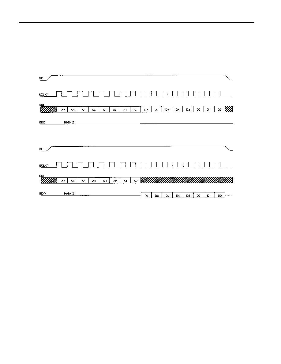
TIMING DIAGRAM: SPI READ DATA TRANSFER
Figure 11

DS1722
12 of 13
TIMING DIAGRAM: SPI WRITE DATA TRANSFER
Figure 12
*SCLK can be either polarity, timing shown for CPOL = 1.
NOTES:
1. All voltages are referenced to ground.
2. Logic 0 voltages are specified at a sink current of 4 mA.
3. Logic 1 voltages are specified at a source current of 1 mA.
4. I
CC
specified with SCLK=V
DDD
and CE=GND. Typical I
CC1
is 0.25 µA and I
CC
is 0.3 mA at 25∞C
and V
DDD =
2.65V
.
5. Measured at V
IH
=0.7 V
DDD
or V
IL
=0.2 V
DDD
and 10 ms maximum rise and fall time.
6. Measured with 50 pF load
7. Measured at V
OH
=0.7 V
DDD
or V
OL
=0.2 V
DDD
. Measured from the 50% point of SCLK to the V
OH
minimum of SDO.
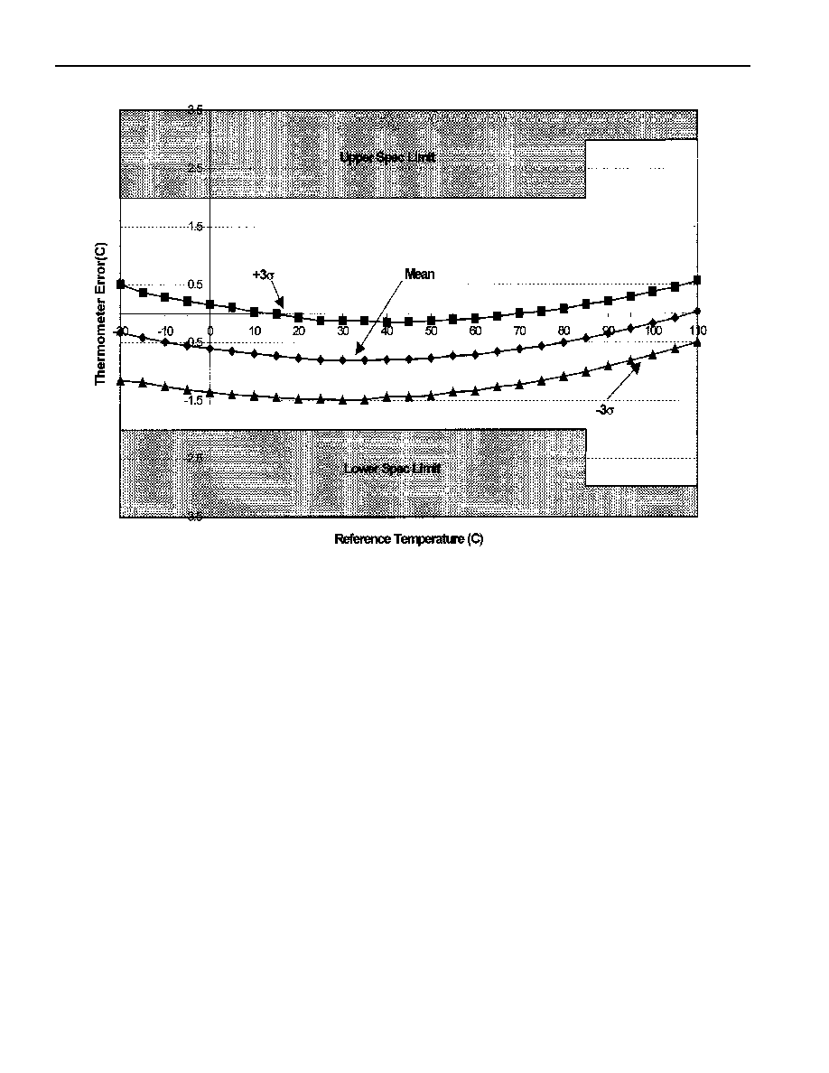
8. Figure 13 shows mean thermometer error for a pre-characterization sample. Data covering a larger
sample over the full temperature range is pending.
DS1722
13 of 13
TYPICAL DS1722 THERMOMETER ERROR