 | ÐлекÑÑоннÑй компоненÑ: DS3100DK | СкаÑаÑÑ:  PDF PDF  ZIP ZIP |
Äîêóìåíòàöèÿ è îïèñàíèÿ www.docs.chipfind.ru
1 of 32
REV: 110206
GENERAL DESCRIPTION
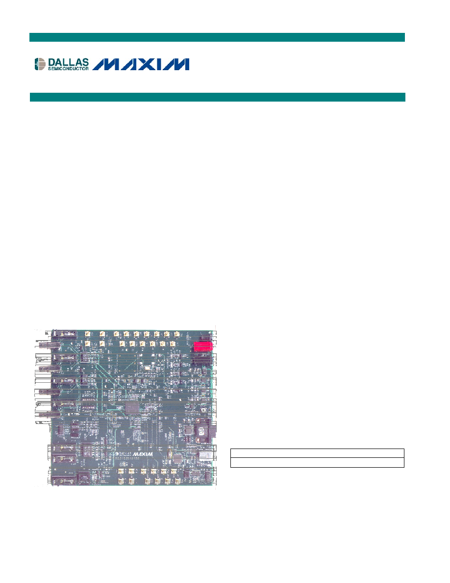
The DS3100DK is an easy-to-use demo and
evaluation kit for the DS3100 Stratum 3/3E timing
card IC. A surface-mounted DS3100 and careful
layout provide maximum signal integrity. An on-board
Dallas 8051-compatible microcontroller and included
software give point-and-click access to configuration
and status registers from a personal computer. LEDs
on the board indicate interrupt, power-supply
function, and GPIO status. The board provides BNC
and bantam connectors for the composite clock and
BITS interfaces. Single-ended and LVDS clocks are
accessed via SMB connectors. All LEDs and
connectors are clearly labeled with silkscreening to
identify associated signals.
DEMO KIT CONTENTS
DS3100DK PCB
CD_ROM Includes:
DS3100 Software
DS3100 Initialization File
DS3100DK Data Sheet
DS3100 Data Sheet/Errata Sheet
FEATURES
Soldered DS3100 for Best Signal Integrity
SMB Connectors, BNC, Bantam,
Transformers, and Termination Ease
Connectivity
Careful Layout for Analog Signal Paths
On-Board Stratum 3 Oscillator with Footprints
for Stratum 3E Oscillators
DS3100 Configured for CPU Bus Operation
for Complete Control Over the Device
On-Board Dallas Microcontroller and Included
Software Provide Point-and-Click Access to
the DS3100 Register Set
LEDs for Interrupt, Power Supplies, and GPIO
Included International Power Supply
Banana Jack VDD and GND Connectors
Support Use of Lab Power Supplies
Easy-to-Read Silkscreen Labels Identify the
Signals Associated with All Connectors,
Jumpers and LEDs
Header Provided for Master/Slave Connection
to a Second DS3100DK
Software Provides GUI Fields for Most
Commonly Used Features Plus Full
Read/Write Access to the Entire Register Set
Software Support for Creating and Running
Configuration Scripts Saves Time During
Evaluation
MINIMUM SYSTEM REQUIREMENTS
PC Running Windows® XP or Windows 2000
Display with 1024 x 768 Resolution or Higher
Available Serial (COM) Port
DB-9 Serial Cable
ORDERING INFORMATION
PART DESCRIPTION
DS3100DK
Demo kit for DS3100
DS3100DK
Stratum 3/E3 Timing Card IC
Demo Kit
www.maxim-ic.com
Windows is a registered trademark of Microsoft Corp.

DS3100DK
2 of 32
TABLE OF CONTENTS
1.
BOARD FLOORPLAN........................................................................................................4
1.1
I
NPUT AND
O
UTPUT
C
LOCKS
............................................................................................................5
1.2
J
UMPERS
, H
EADERS
,
AND
S
WITCH
S
ETTINGS
..................................................................................5
1.3
C
OMPOSITE
C
LOCK
I
NTERFACE
.......................................................................................................5
1.4
BITS
I
NTERFACES
...........................................................................................................................5
1.5
M
ICROCONTROLLER
........................................................................................................................5
1.6
P
OWER
-S
UPPLY
C
ONNECTORS
........................................................................................................5
2.
BASIC HARDWARE SETUP..............................................................................................6
3.
INSTALLING AND RUNNING THE SOFTWARE...............................................................6
3.1
C
OMMAND
L
INE
O
PTIONS
................................................................................................................6
4.
OVERVIEW OF THE SOFTWARE INTERFACE................................................................7
4.1
G
LOBAL
C
ONFIGURATION
................................................................................................................7
4.2
I
NPUT
C
LOCK
M
ONITOR
, D
IVIDER
,
AND
S
ELECTOR
...........................................................................7
4.3
T0 DPLL ........................................................................................................................................8
4.4
T4 DPLL ........................................................................................................................................9
4.5
T0 APLL.......................................................................................................................................10
4.6
T4 APLL.......................................................................................................................................10
4.7
O
UTPUT
C
LOCKS
...........................................................................................................................11
4.8
DPLL F
REQUENCY
L
IMITS
, P
HASE
D
ETECTORS
, DPLL L
OCK
C
RITERIA
..........................................12
4.9
BITS R
ECEIVERS AND
BITS T
RANSMITTERS
..................................................................................13
4.9.1
Note About Working with the BITS Receivers and Transmitters ......................................................... 13
4.10
C
OMPOSITE
C
LOCK
R
ECEIVERS
.................................................................................................14
4.11
REFCLK C
ALIBRATION
..............................................................................................................14
4.12
R
EGISTER
V
IEW
W
INDOW
...........................................................................................................14
4.13
C
ONFIGURATION
S
CRIPTS AND
L
OG
F
ILE
....................................................................................15
4.13.1
Configuration Log File.......................................................................................................................... 15
4.13.2
Configuration Scripts............................................................................................................................ 15
5.
ADDITIONAL INFORMATION AND RESOURCES .........................................................15
5.1
DS3100 I
NFORMATION
..................................................................................................................15
5.2
DS3100DK I
NFORMATION
.............................................................................................................15
5.3
T
ECHNICAL
S
UPPORT
....................................................................................................................15
6.
APPENDIX 1: HARDWARE COMPONENTS...................................................................16
7.
APPENDIX 2: BITS MODE WRITE SEQUENCES...........................................................19
8.
SCHEMATICS ..................................................................................................................19
9.
DOCUMENT REVISION HISTORY ..................................................................................19

DS3100DK
3 of 32
LIST OF FIGURES
Figure 1-1. Board Floorplan......................................................................................................................................... 4
LIST OF TABLES
Table 4-1. Mapping Between Input Clock Software Fields and DS3100 Register Fields ........................................... 7
Table 4-2. Mapping Between T0 DPLL Software Fields and DS3100 Register Fields ............................................... 8
Table 4-3. Mapping Between T4 DPLL Software Fields and DS3100 Register Fields ............................................... 9
Table 4-4. Mapping Between T0 APLL Software Fields and DS3100 Register Fields ............................................. 10
Table 4-5. Mapping Between T4 APLL Software Fields and DS3100 Register Fields ............................................. 10
Table 4-6. Mapping Between Output Clock Software Fields and DS3100 Register Fields ...................................... 11
Table 4-7. Mapping Between DPLL Software Fields and DS3100 Register Fields .................................................. 12
Table 4-8. Mapping Between BITS Software Fields and DS3100 Register Fields ................................................... 13
Table 4-9. Mapping Between CC Software Fields and DS3100 Register Fields ...................................................... 14
Table 4-10. Mapping Between REFCLK Software Fields and DS3100 Register Fields ........................................... 14
DS3100DK
4 of 32
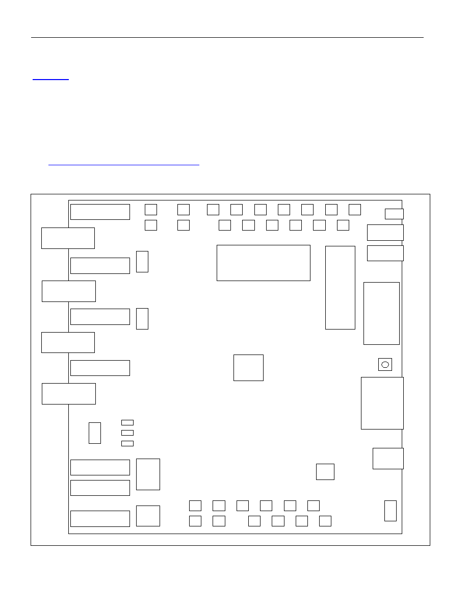
1. BOARD
FLOORPLAN
Figure 1-1
shows the floorplan of the DS3100DK. The DS3100 is in the center of the board, input clock SMB
connectors are along the top edge of the board, and output clock connectors are on the bottom edge. Between the
input clock connectors and the DS3100, land patterns are provided for several different types of local oscillators,
ranging from tiny, inexpensive TCXOs to larger, high-performance OCXOs. The right edge contains, from top to
bottom, power supply connectors, DC-DC converters and power-indicator LEDs, reset push-button, serial
connector and USB connector. An on-board DS87C520 microcontroller is located near the USB connector. The left
edge of the board is occupied by connectors and transformers for the DS3100's built-in BITS (DS1/E1/2048kHz)
and composite clock (64kHz) receivers and transmitters. Between the BITS and composite clock connectors are a
JTAG header and three switches to control the DS3100's MASTSLV, SONSDH, and SRCSW pins.
See
APPENDIX 1: HARDWARE COMPONENTS
for a complete component list. Complete board schematics follow
Appendix 2.
Figure 1-1. Board Floorplan
`
Power
Option
5V Banana
Jack
GND Banana
Jack
R
S
232 9-
P
i
n
C
onnec
t
or
US
B
C
onne
ct
or
GP
I
O
Ci
r
c
u
i
t
r
y
P
o
w
er
S
uppl
y
C
i
r
c
ui
t
r
y
LVDS Output
Clocks
Microprocessor
DS3100
Single-ended Output Clocks
C
om
pos
i
t
e C
l
oc
k
In
p
u
t
C
om
p
os
i
t
e
C
l
oc
k
O
ut
put
JTAG
Header
B
IT
S
In
te
rfa
c
e
s
Oscillator Circuitry
Single-ended Input Clocks
LVDS Input
Clocks
M\
S
Hd
r
Switches
Reset

DS3100DK
5 of 32
1.1
Input and Output Clocks
There are 13 SMB connectors at the top of the board labeled IC1IC4, IC7IC14, and SYNC2K that provide a
single-ended clock input to the DS3100. All single-ended clock inputs are connected to the DS3100 with a 50
characteristic impedance trace and terminated with 50
at the device. Four additional SMB connectors labeled
IC5P, IC5N, IC6P, and IC6N provide differential clock inputs to the DS3100. These differential inputs have 50
trace impedance and 50
termination at the device (i.e., 100
differential).
On the other end of the PCB are eight SMB clock output connectors labeled OC1OC5 and OC9, OC10, and
OC11. All single-ended clock outputs are buffered at the DS3100 and connected to the SMB connector via a 50
characteristic impedance trace. Four additional SMB connectors labeled OC6P, OC6N, OC7P, and OC7N provide
connections to the differential outputs from the DS3100.
1.2 Jumpers,
Headers, and Switch Settings
Jumpers JMP1 to JMP4 (upper right of board) provide input settings to the four DS3100 GPIO pins. If a jumper is
installed the corresponding GPIO input is high. With no jumper the GPIO pin defaults low. LEDs DS5DS8 indicate
the logic level of the GPIO pins (LED lit means GPIO pin is high). Switches SW7 to SW9 set the SONSDH,
SRCSW and MASTSLV pins, respectively, high or low as indicated by the silkscreen. Headers J1 and J2 provide
access to BITS1 and BITS2 framer signals, respectively. Header J51 provides access to the JTAG port of the
DS3100. Header J15 provides interface to a master or slave board depending on position of switch SW6.
1.3
Composite Clock Interface
Bantam jacks J89 and J90 provide access to composite clock inputs IC1A and IC2A through a 2:1 transformer.
Jumpers JMP7 and JMP6 configure termination for IC1A and IC2A respectively. Silkscreen text indicates which
jumper is necessary to set the interface at 110
, 120
, or 133
. Bantam jack J117 provides an interface through a
1:1 transformer to the OC8 composite clock output. Jumpers JMP8, JMP9, and JMP10 provide different attenuation
configurations that are represented in silkscreen (Rs = 91
with no jumper installed). See the schematics for
additional details on the composite clock termination circuitry.
1.4 BITS Interfaces
The BITS1 DS1/E1 LIU uses bantam connectors J85 and J55 or BNC connectors J83 and J57 for transmit and
receive interfaces, respectively. The BITS2 LIU uses bantam connectors J86 and J56 or BNC connectors J84 and
J58 for transmit and receive, respectively. There is a dual transformer package for each BITS transceiver
(component T1 for BITS1 and T2 for BITS2). See the schematics for additional details on the BITS termination
circuitry.
1.5 Microcontroller
The DS87C520 microcontroller has factory-installed firmware in on-chip nonvolatile memory. This firmware
translates memory access requests from the RS-232 serial port or USB port into register accesses on the DS3100.
When the microcontroller starts up it turns on DS16 to indicate that the controller is working correctly. A pushbutton
switch labeled RESET (SW5) at the right middle of the board resets the microcontroller as well as the DS3100.
1.6 Power-Supply
Connectors
The included international power supply can be connected to jack J3 to power the board or a 5V lab power supply
can be connected across the red (J13) and black (J19) banana jacks. The 5V input is then regulated to 3.3V and
1.8V and distributed to board components.
Document Outline
- þÿ
- þÿ
- þÿ
- þÿ
- þÿ
- þÿ
- þÿ
- þÿ
- þÿ
- þÿ
- þÿ
- þÿ
- þÿ
- þÿ
- þÿ
- þÿ
- þÿ
- þÿ
- þÿ
- þÿ
- þÿ
- þÿ