 | –≠–ª–µ–∫—Ç—Ä–æ–Ω–Ω—ã–π –∫–æ–º–ø–æ–Ω–µ–Ω—Ç: DS31256DK | –°–∫–∞—á–∞—Ç—å:  PDF PDF  ZIP ZIP |
1 of 31
REV: 052703
GENERAL DESCRIPTION
The DS31256DK is a demonstration and evaluation
kit for the DS31256 Envoy 256-channel, high-
throughput HDLC controller. The DS31256DK board
is a PCI-based platform that offers quick and easy
evaluation of the DS31256 HDLC controller, low-cost
prototyping, and rapid software development. The
DS31256DK operates with a software suite that runs
under Microsoft Windows
Æ
95/98/NT. The PC platform
must be at least a 200MHz+ Pentium II class CPU
with 32MB of RAM.
Windows is a registered trademark of Microsoft Corp.
ORDERING INFORMATION
PART DESCRIPTION
DS31256 Demonstration
Kit
FEATURES
ß Headers Provide Access to Clock, Sync, and
Data for 16 Physical Ports
ß Full Source Code
ß Windows/Windows NT GUI for Device
Configuration and Evaluation
ß Programmable PLD for Port Connectivity and
Clock Generation
ß Local Bus Header for Control and Configuration
of External Devices
ß Hardware Prototyping Area
DEMO KIT CONTENTS
CD-ROM Includes:
HDLC Application Notes
DS31256DK Data Sheet/Manual
Installation Guide
DS31256 Data Sheet
Executable Evaluation Application
Source Code for Driver and GUI Application
DS31256DK
256-Channel, High-Throughput
HDLC Controller Demonstration Kit
www.maxim-ic.com

DS31256 Demonstration Kit
2 of 31
TABLE OF CONTENTS
1.
GENERAL OVERVIEW ................................................................................................................. 3
2.
SOFTWARE ................................................................................................................................ 10
2.1
A
RCHITECTURE
.......................................................................................................................... 10
2.2
I
NTRODUCTION TO
C
HAT
............................................................................................................. 10
2.3
C
HAT
GUI.................................................................................................................................. 11
2.3.1
Main GUI Interface--Configuration..................................................................................... 11
2.3.2
Show Results ..................................................................................................................... 17
2.3.3
Memory Viewer .................................................................................................................. 19
2.3.4
DMA Configuration............................................................................................................. 20
2.3.5
Register Access ................................................................................................................. 21
2.4
D
RIVER
...................................................................................................................................... 22
3.
INSTALLATION AND GETTING STARTED................................................................................ 23
3.1
C
ARD
I
NSTALLATION
................................................................................................................... 23
3.1.1
Windows 95 Systems ......................................................................................................... 23
3.1.2
Windows 98 Systems ......................................................................................................... 23
3.1.3
Windows NT Systems ........................................................................................................ 24
3.2
S
OFTWARE
I
NSTALLATION
........................................................................................................... 24
3.3
O
PERATIONAL
T
EST
.................................................................................................................... 24
4.
APPENDIX A............................................................................................................................... 25

DS31256 Demonstration Kit
3 of 31
LIST OF FIGURES
Figure 1-1. PCI Card Configuration........................................................................................................ 5
Figure 1-2. Port PLD Schematic ............................................................................................................ 6
Figure 2-1. Software Architecture ........................................................................................................ 10
Figure 2-2. Software Main GUI ............................................................................................................ 11
Figure 2-3. Show Results GUI ............................................................................................................. 17
Figure 2-4. Memory Viewer GUI .......................................................................................................... 19
Figure 2-5. DMA Configuration GUI..................................................................................................... 20
Figure 2-6. Registers Access GUI ....................................................................................................... 21
Figure 2-7. Low-Level API Source Block Relationships ....................................................................... 22
LIST OF TABLES
Table 1-A. Header A Definition .............................................................................................................. 7
Table 1-B. Header B Definition .............................................................................................................. 8
Table 1-C. Header C Definition.............................................................................................................. 9
Table 2-A. Low-Level API Source Block Contents ............................................................................... 22

DS31256 Demonstration Kit
4 of 31
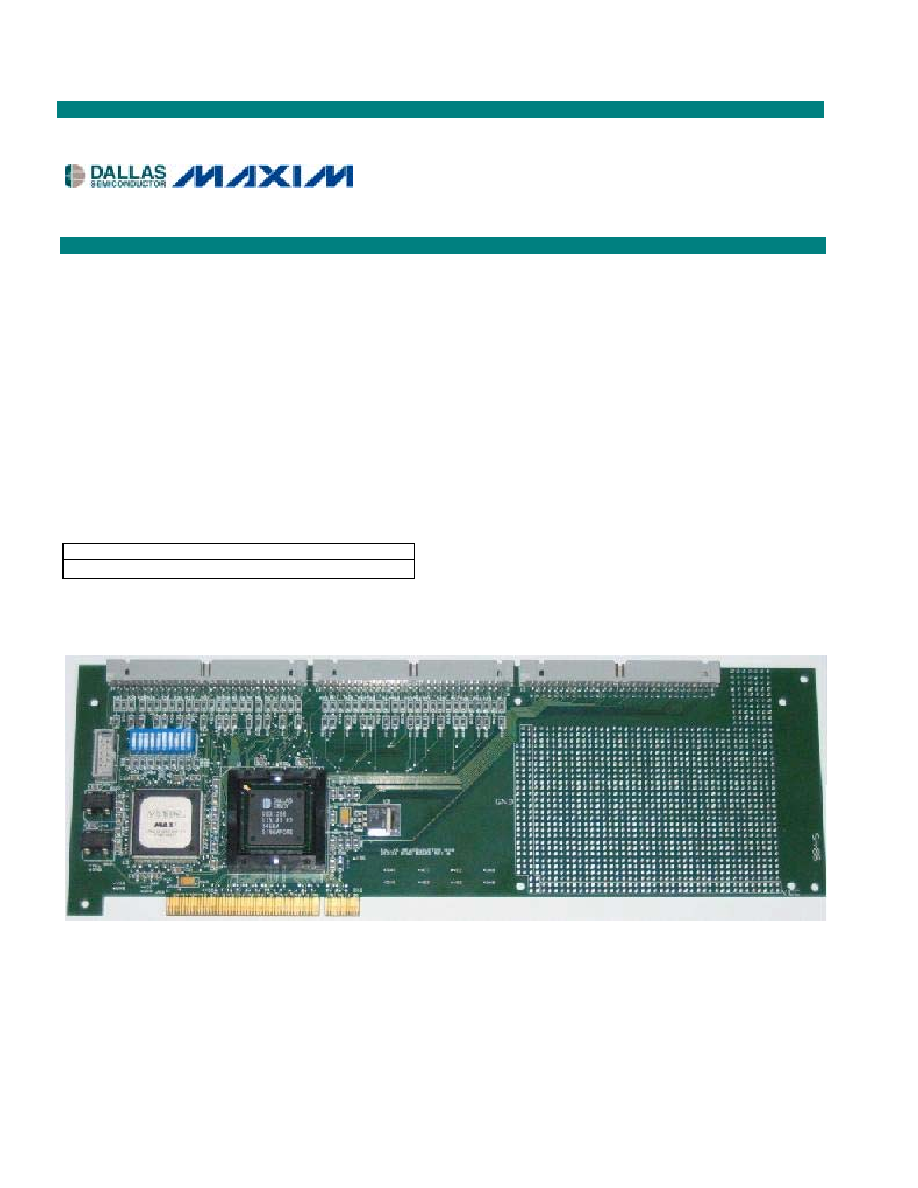
1. GENERAL OVERVIEW
The DS31256DK is a demonstration and evaluation kit for the DS31256 Envoy 256-channel, high-throughput
HDLC controller. The DS31256DK is intended to be used in a full-size PC platform, complete with PCI. The
DS31256DK operates with a software suite that runs under Microsoft Windows 95/98/NT. The PC platform must be
at least a 200MHz+ Pentium II class CPU with 32MB of RAM.
Figure 1-1
details an outline of the PCI board for the
DS31256DK.
The DS31256DK was designed to be as simple as possible but offers the flexibility to be used in a number of
different configurations. The DS31256DK has all the DS31256's port and local bus pins, which are easily
accessible through headers on top of the card. A second DS31256DK can also be loaded into the PC in an
adjacent PCI slot to add additional functions such as:
ß Multiple T1/E1 framers
ß T3 line interface
ß HSSI interface
ß V.35 interfaces
An Altera 9000 series PLD device is connected to all port pins on the DS31256. The PLD can be loaded with
various configurations through a programming port (J4) that resides on the DS31256DK. This PLD generates
clocks and frame syncs as well as routes data from one port to another in a daisy-chain fashion to allow testing the
device under worst-case loading (
Figure 1-2
). Two oscillators provide the port timing.
The transmit side of a port is derived from one clock and the receive side from another, so that they can be
asynchronous to one another. If the PLD is not needed, it can be tri-stated to remove it (electrically) from the
board. Signals can then be sent to the DS31256 by the pin headers.
The board is intended to be a full-size PCI card that can only be plugged into a 5V PCI system environment. There
is a 256-pin plastic BGA socket on the board for the DS31256.
Only the DS31256 operates at 3.3V. Since it cannot be guaranteed that a 3.3V supply exists in a 5V PCI system
environment, the DS31256DK has a linear regulator on it (U4: LT1086) to convert from 5V to 3.3V. All of the other
logic, including the PLD and oscillators, operate at 5V. If 3.3V exists on the PCI bus, the linear regulator can be
removed and a 0
W jumper can be installed at R97 (
Figure 1-1
).
The JTAG pins on the DS31256 are not active on the DS31256DK. Therefore, the JTCLK, JTDI, and JTMS signals
are wired to 3.3V and
JTRST is wired low.

DS31256 Demonstration Kit
5 of 31
Figure 1-1. PCI Card Configuration
J3: HEADER C
(60 PINS)
LOCAL BUS
PLUS 12 GROUNDS
(SEE TABLE 1-C)
U4: LT1086CM-3.3
5V to 3.3V
Linear Reg.
OSC
SW1:
10 Position
DIP Switch
to Ground
U3: PORT PLD
ALTERA 9000
100k
W PULLDOWN
ON RD/RC/TC
OSC
100k
W PULLUPS TO 3.3V ON
LINT/LCS/LRDY/LHLDA/LIM 100k
W
PULLDOWNS ON LMS
V
DD
PCI
BUS
28 PORTS
LOCAL
BUS
J4: PLD
PROGRAMMING
PORT
demokit2
PCI
TEST
POINTS
10
100k
W PULLUP
TO 5V
8-PIN CAN
OSCILLATORS
(SOCKETED)
5
5V
3.3V
R97
JTMS
JTCLK
JRST
JDI
V
SS
V
DD
V
DD
V
DD
JTDO
OPEN
PROTOTYPE AREA
(AN ARRAY OF VIAS
ON A 100-MIL PITCH)
J2: HEADER B
(72 PINS)
PORTS 8 TO 15
PLUS 12 GROUNDS
(SEE TABLE 1-B)
J2: HEADER A
(72 PINS)
PORTS 0 TO 7
PLUS 12 GROUNDS
(SEE TABLE 1-A)
100k
W PULLDOWN
ON RD/RC/TC
U1: DS31256
256-PIN BGA
SOCKET