 | –≠–ª–µ–∫—Ç—Ä–æ–Ω–Ω—ã–π –∫–æ–º–ø–æ–Ω–µ–Ω—Ç: DS3131DK1 | –°–∫–∞—á–∞—Ç—å:  PDF PDF  ZIP ZIP |
1 of 33
111802
Note: Some revisions of this device may incorporate deviations from published specifications known as errata. Multiple revisions of any device
may be simultaneously available through various sales channels. For information about device errata, click here:
www.maxim-ic.com/errata
.
GENERAL DESCRIPTION
The DS3131 bit-synchronous (BoSS) HDLC
controller can handle up to 40 channels of high-
speed, unchannelized, bit-synchronous HDLC.
The on-board DMA has been optimized for
maximum flexibility and PCI bus efficiency to
minimize host processor intervention in the data
path. Diagnostic loopbacks and an on-board
BERT remove the need for external components.
APPLICATIONS
Routers
xDSL Access Multiplexers (DSLAMs)
Clear-Channel (unchannelized) T1/E1
Clear-Channel (unchannelized) T3/E3
SONET/SDH Path Overhead Termination
High-Density V.35 Terminations
High-Speed Links such as HSSI
FEATURES
ß 40 Timing Independent Ports
ß 40 Bidirectional HDLC Channels
ß Each Port Can Operate Up to 52Mbps
ß Up to 132Mbps Full-Duplex Throughput
ß On-Board Bit Error-Rate Tester (BERT)
ß Diagnostic Loopbacks in Both Directions
ß Local Bus Supports PCI Bridging
ß 33MHz 32-Bit PCI Interface
ß Full Suite of Driver Code
ORDERING INFORMATION
PART TEMP
RANGE PIN-PACKAGE
DS3131
0∞C to +70∞C
272 PBGA
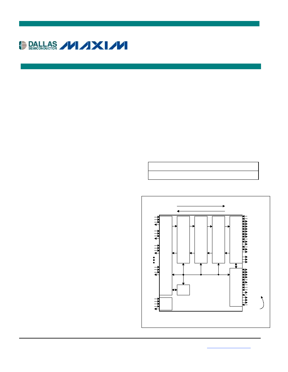
FUNCTIONAL DIAGRAM
DS3131DK
Bit-SynchronouS (BoSS)
HDLC Controller Demo Kit
www.maxim-ic.com
PIN NAMES IN ( )
ARE ACTIVE WHEN
THE DEVICE IS IN
THE MOT MODE
(i.e., LIM = 1).
RC2
RD2
TC2
TD2
JTDO
PCLK
PAD[31:0]
PRST
PCBE[3:0]
PPAR
PFRAME
PIRDY
PTRDY
PSTOP
PIDSEL
PDEVSEL
PREQ
PGNT
PPERR
PSERR
RC39
RD39
TC39
TD39
RC0
RD0
TC0
TD0
RC1
RD1
TC1
TD1
PXAS
PXDS
PXBLAST
JTRST
JTDI
JTMS
JTCLK
LA[19:0]
LD[15:0]
LWR(LR/W)
LRD(LDS)
LIM
LINT
LRDY
LMS
LCS
LHOLD(LBR)
LHLDA(
LBG)
LBGACK
LCLK
LBHE
JTAG TEST
ACCESS
LO
CA
L B
U
S
B
L
O
C
K
L
AYER
1
BL
O
C
K
40-
B
I
T
S
Y
NCHRO
NO
U
S
HDLC CO
NT
R
O
LLE
RS
FI
FO
B
L
OC
K
D
M
A BL
O
C
K
PC
I
BL
O
C
K
BERT
RECEIVE DIRECTION
TRANSMIT DIRECTION
INTERNAL CONTROL BUS
LBPXS
DS3131

DS3131DK
2 of 33
TABLE OF CONTENTS
1.
GENERAL OVERVIEW................................................................................................................. 3
Figure 1-1. PCI Card Configuration ............................................................................................................. 4
Figure 1-2. Port PLD Schematic................................................................................................................... 5
Table 1-A. Header A Definition ................................................................................................................... 6
Table 1-B. Header B Definition.................................................................................................................... 7
Table 1-C. Header C Definition.................................................................................................................... 8
2.
SOFTWARE ..................................................................................................................................... 9
2.1 A
RCHITECTURE
................................................................................................................................ 9
Figure 2-1. Software Architecture ................................................................................................................ 9
2.2 I
NTRODUCTION TO
B
O
SS.................................................................................................................. 9
2.3 B
O
SS S
OFTWARE
GUI I
NTERFACE AND
D
ESCRIPTION
................................................................... 11
2.3.1 Main GUI Interface--Configuration ...................................................................................... 11
Figure 2-2. Software Main GUI.................................................................................................................. 11
2.3.2 Show Results ........................................................................................................................... 15
Figure 2-3. Show Results GUI (Driver Statistics) ...................................................................................... 15
Figure 2-4. Show Results GUI (Application Statistics).............................................................................. 16
Figure 2-5. Show Results GUI (BoSS Statistics) ....................................................................................... 17
2.3.3 Memory Viewer....................................................................................................................... 18
Figure 2-6. Memory Viewer GUI............................................................................................................... 18
2.3.4 Register Access ....................................................................................................................... 19
Figure 2-7. Registers Access GUI .............................................................................................................. 19
2.3.5 DMA Configuration ................................................................................................................ 20
Figure 2-8. DMA Configuration GUI......................................................................................................... 20
2.4 D
RIVER
........................................................................................................................................... 22
Table 2-A. Low-Level API Source Block Contents................................................................................... 22
Figure 2-9. Low-Level API Source Block Relationships........................................................................... 23
3.
INSTALLATION AND GETTING STARTED .......................................................................... 24
3.1 C
ARD
I
NSTALLATION
...................................................................................................................... 24
3.1.1 Windows 95 Systems ............................................................................................................... 24
3.1.2 Windows 98 Systems ............................................................................................................... 25
3.1.3 Windows NT Systems .............................................................................................................. 25
3.2 S
OFTWARE
I
NSTALLATION
............................................................................................................. 26
3.3 O
PERATIONAL
T
EST
....................................................................................................................... 26
4.
PC BOARD LAYOUT ................................................................................................................... 27
5.
APPENDIX A.................................................................................................................................. 28

DS3131DK
3 of 33
1. GENERAL OVERVIEW
The DS3131DK is a demonstration and evaluation kit for the DS3131 BoSS bit-synchronous HDLC
controllers. The DS3131DK is intended to be used in a full-size PC platform, complete with PCI. The
DS3131DK operates with a software suite that runs under Microsoft Windows
Æ
95/98/NT. The PC
platform must be at least a 200MHz+ Pentium II class CPU with 32MB of RAM.
Figure 1-1
details an
outline of the PCI board for the DS3131DK.
The DS3131DK was designed to be as simple as possible but provides the flexibility to be used in a
number of different configurations. The DS3131DK has all of the port pins and the local bus pins from
the DS3131 that are easily accessible through headers on top of the card. A second DS3131DK can also
be loaded into the PC in an adjacent PCI slot to add additional functions such as:
ß Multiple T1/E1 framers
ß T3 line interface
ß HSSI interface
ß V.35 interfaces
An Altera 9000 series PLD device is connected to all of the port pins on the DS3131. The PLD is capable
of being loaded with various configurations through a programming port (J4) that resides on the
DS3131DK. This PLD generates clocks and frame syncs as well as routes data from one port to another
in a daisy-chain fashion to allow testing the device under worst-case loading (
Figure 1-2
). Two
oscillators provide the port timing.
The transmit side of a port is derived from one clock and the receive side from another, so that they can
be asynchronous to one another. If the PLD is not needed, it can be three-stated to remove it (electrically)
from the board. Signals can then be sent to the DS3131 by the pin headers.
The board is intended to be a full-size PCI card that can only be plugged into a 5V PCI system
environment. There is a 256-pin plastic BGA socket on the board for the DS3131.
Only the DS3131 is operated at 3.3V. Since it cannot be guaranteed that a 3.3V supply exists in a 5V PCI
system environment, the DS3131DK has a linear regulator on it (U4: LT1086) to convert from 5V to
3.3V. All of the other logic, including the PLD and oscillators, operate at 5V. If 3.3V exists on the PCI
bus, the linear regulator can be removed and a 0 jumper can be installed at R97 (
Figure 1-1
).
The JTAG pins on the DS3131 are not active on the DS3131DK. Therefore, the JTCLK, JTDI, and JTMS
signals are wired to 3.3V and JTRST is wired low.
The DS3131DK was designed to use the device's 28-port mode rather than the 40-port mode, so the local
bus can be used.
Windows is a registered trademark of Microsoft Corp.

DS3131DK
4 of 33
Figure 1-1. PCI Card Configuration
J3: Header C
(60 Pins)
Local Bus
Plus 12 Grounds
(see Table 1C)
J2: Header B
(72 Pins)
Ports 8 to 15
Plus 12 Grounds
(see Table 1B)
J1: Header A
(72 Pins)
Ports 0 to 7
Plus 12 Grounds
(see Table 1A)
U1: DS3131
256 Pin
BGA Socket
U4: LT1086CM-3.3
5V to 3.3V
Linear Reg.
Osc.
SW1:
10 Position
DIP Switch
to Ground
U3:
Port PLD
Altera 9000
100K Pull Down
on RD / RC /TC
100K Pull Down
on RD / RC / TC
Osc.
100K Pull Ups to 3.3V on
LINT / LCS / LRDY / LHLDA / LIM
100K Pull Downs on LMS
VDD
PCI
Bus
28 Ports
Local
Bus
J4: PLD
Programming
Port
demokit2
PCI Test
Points
10
100K PU to 5V
8-pin
Can Oscillators
(socketed)
5
5V
3.3V
R97
JTMS
JTCLK
JRST
JDI
VSS
VDD
VDD
VDD
JTDO
open
Prototype Area
(an array of vias
on a 100 mil pitch)

DS3131DK
5 of 33
Figure 1-2. Port PLD Schematic
RC
RD
TD
TC
Altera PLD
DS3131
Port 0
RC
RD
TC
TD
Port 1
RC
RD
TD
TC
Port 2
RC
RD
TC
TD
Port 3
RC
RD
TD
TC
Port 26
RC
RD
TC
TD
Port 27
Divide by
2 / 6 / 8 /
16 / 32 / 42
Divide by
2 / 6 / 8 /
16 / 32 / 42
Mux
Mux
SW10:
0 = outputs tri-state
1 = outputs enabled
Clock
#1
Clock
#2
SW1/SW2/SW3:
Clock/Sync Select
(see below)
SW5:
0 = sync normal
1 = force sync low
DIP Switch
Notes:
1. Switches 6 to 8
have no assignment
2. The default state
for all switches = 1
(See Clock/Sync
Definition Table Below:)
SW9:
0 = OFF
1 = ON
(Diagram show SW9 =1)
SW4:
0 = port 0/1 slow clock
1 = port 0/1 fast clock
Clock/Sync Definitions
SW3 SW2 SW1 Clock Speed with OSC = 66MHz
0
0
0
66MHz / 2 = 33MHz
0
0
1
66MHz / 6 = 11.00MHz
0
1
0
66MHz / 8 = 8.25MHz
0
1
1
66MHz / 16 = 4.125MHz
1
0
0
66MHz / 32 = 2.0625MHz
1
0
1
66MHz / 42 = 1.572MHz
Note 1: Switch Open = Off = High (1)
Note 2: Switch Closed = On = Low (0)