 | –≠–ª–µ–∫—Ç—Ä–æ–Ω–Ω—ã–π –∫–æ–º–ø–æ–Ω–µ–Ω—Ç: MAX132 | –°–∫–∞—á–∞—Ç—å:  PDF PDF  ZIP ZIP |
_______________General Description
The MAX132 is a CMOS, 18-bit plus sign, serial-output,
analog-to-digital converter (ADC). Multi-slope integra-
tion provides high-resolution conversions in less time
than standard integrating ADCs, allowing operation up
to 100 conversions per second. Low conversion noise
provides guaranteed operation with ±512mV full-scale
input range (2µV/LSB). A simple 4-wire serial interface
connects easily to all common microprocessors, and
twos-complement output coding simplifies bipolar mea-
surements. Typical supply current is only 60µA and is
reduced to 1µA in sleep mode. Four serially pro-
grammed digital outputs can be used to control an
external multiplexer or programmable-gain amplifier.
The MAX132 comes in 24-pin narrow DIP and wide SO
packages, and is available in commercial and extend-
ed temperature grades.
High resolution, compact size, and low power make this
device ideal for data loggers, weigh scales, data-acqui-
sition systems, and panel meters.
________________________Applications
Remote Data Acquisition
Battery-Powered Instruments
Industrial Process Control
Transducer-Signal Measurement
Pressure, Flow, Temperature, Voltage
Current, Resistance, Weight
____________________________Features
o
Low Supply Current:
60µA (Normal Operation)
1µA (Sleep-Mode Operation)
o
±0.006% FSR Accuracy at 16 Conv/sec
o
Low Noise: 15µV
RMS
o
Serial I/O Interface with Programmed Output for
Mux and PGA
o
Performs up to 100 Conv/sec
o
±2pA Input Current
o
50Hz/60Hz Rejection
MAX132
±18-Bit ADC with Serial Interface
________________________________________________________________
Maxim Integrated Products
1
24
23
22
21
20
19
18
17
1
2
3
4
5
6
7
8
V+
BUF OUT
INT OUT
INT IN
SCLK
DOUT
DIN
CS
TOP VIEW
CREF-
CREF+
REF+
REF-
P1
P0
OSC1
OSC2
16
15
14
13
9
10
11
12
AGND
IN LO
IN HI
V-
DGND
EOC
P3
P2
DIP/SO
MAX132
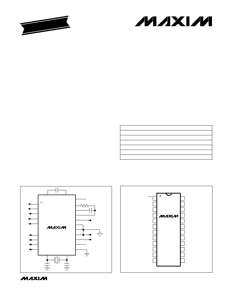
__________________Pin Configuration
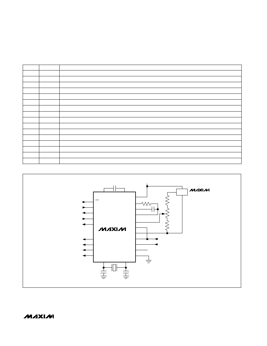
MAX132
CREF-
CREF+
CS
602k
SCLK
DOUT
DIN
EOC
P0
P1
P2
P3
-5V
±512mV INPUT
BUF OUT
INT OUT
INT IN
4.7nF
REF+
REF-
AGND
IN LO
IN HI
V-
V+
DGND
OSC2
OSC1
+5V
________________Functional Diagram
Call toll free 1-800-998-8800 for free samples or literature.
19-0009; Rev 2; 8/95
PART
MAX132CNG
MAX132CWG
MAX132C/D
0∞C to +70∞C
0∞C to +70∞C
0∞C to +70∞C
TEMP. RANGE
PIN-PACKAGE
24 Narrow Plastic DIP
24 Wide SO
Dice*
EVALUATION KIT MANUAL
FOLLOWS DATA SHEET
______________Ordering Information
* Contact factory for dice specifications.
** Contact factory for availability and processing to MIL-STD-883.
MAX132ENG
MAX132EWG
MAX132MRG
-55∞C to +125∞C
-40∞C to +85∞C
-40∞C to +85∞C
24 Narrow Plastic DIP
24 Wide SO
24 Narrow CERDIP**
MAX132
±18-Bit ADC with Serial Interface
2
_______________________________________________________________________________________
ABSOLUTE MAXIMUM RATINGS
ELECTRICAL CHARACTERISTICS
(V+ = 5V, V- = -5V, DGND = AGND = IN LO = REF- = 0V, REF+ = 545mV, R
INT
= 602k
, C
INT
= 0.0047µF, C
REF
= 0.1µF,
f
CLK
= 32,768Hz, 60Hz mode, T
A
= T
MIN
to T
MAX
, unless otherwise noted.)
Stresses beyond those listed under "Absolute Maximum Ratings" may cause permanent damage to the device. These are stress ratings only, and functional
operation of the device at these or any other conditions beyond those indicated in the operational sections of the specifications is not implied. Exposure to
absolute maximum rating conditions for extended periods may affect device reliability.
Supply Voltage
V+ to DGND ..............................................-0.3V < V+ < +6.0V
V- to DGND ................................................+0.3V < V- < -9.0V
V+ to V- ............................................................................+15V
Analog Input Voltage (any input).....................................V+ to V-
Digital Input Voltage .....................(DGND - 0.3V) to (V+ + 0.3V)
Continuous Power Dissipation
Narrow Plastic DIP (derate 8.70mW/∞C above +70∞C)....478mW
Wide SO (derate 11.76mW/∞C above +70∞C)..............647mW
Narrow CERDIP (derate 12.50mW/∞C above +70∞C) ..688mW
Operating Temperature Ranges
MAX132C_ _ .......................................................0∞C to +70∞C
MAX132E_ _ ....................................................-40∞C to +85∞C
MAX132MRG .................................................-55∞C to +125∞C
Storage Temperature Range .............................-65∞C to +160∞C
Lead Temperature (soldering, 10sec) .............................+300∞C
Bits
±18
Resolution
UNITS
MIN
TYP
MAX
PARAMETER
(Note 1)
CONDITIONS
V
IN
HI = 0V
% of FSR
±0.0168
0
±0.0076
Zero Error
f
CLK
= 32.768Hz
(Note 4)
ms
63
±0.032
Rollover Error
(Notes 2, 3)
% of FSR
0
±0.010
% of FSR
±0.0015
±0.006
Integral Nonlinearity
IN HI = IN LO
V
±3.0
Input Voltage Range
Common-Mode Range
(Note 3)
ppm/∞C
±5
Scale Factor Temp. Coefficient
(Note 3)
ppm/∞C
±0.15
±1.5
µV
15
RMS Noise
Zero-Reading Drift
mV
±512
Conversion Time
V
IN
HI = 400mV, V- = -5.0V,
4.5V
V+
5.5V
±0.003
±0.0168
% of FSR
±0.003
±0.0061
Positive Supply Rejection
Digital input = 0V or V+
Digital input = 0V or V+
µA
1
10
µA
-25
-60
Digital Ground Supply Current
Positive Sleep-Mode Current
Digital input = 0V or V+
Digital input = 0V or V+
µA
-35
-65
µA
60
125
Positive Supply Current
Negative Supply Current
Digital input = 0V or V+
µA
-1
-10
Negative Sleep-Mode Current
V
-5.5
-4.5
V
4.5
5.5
Positive Supply Voltage
Negative Supply Voltage
T
A
= +25∞C
T
A
= T
MIN
to T
MAX
T
A
= +25∞C
T
A
= +25∞C
T
A
= T
MIN
to T
MAX
IN HI to IN LO, for specified accuracy
% of FSR
±0.25
±0.50
Common-Mode Rejection Ratio
IN HI = IN LO
±0.009
±0.032
V
CM
= ±500mV
V
CM
= ±3.0V
pA
±12
±250
Leakage Current
IN HI, IN LO
±2
±10
T
A
= +25∞C
T
A
= T
MIN
to T
MAX
T
A
= +25∞C
T
A
= T
MIN
to T
MAX
T
A
= T
MIN
to T
MAX
T
A
= +25∞C
V
IN
HI = 400mV, V- = 5.0V,
-5.5V
V-
-4.5V
±0.003
±0.0168
% of FSR
±0.003
±0.0061
Negative Supply Rejection
Digital input = 0V or V+
µA
0
±2
Digital Ground Sleep-Mode
Current
T
A
= +25∞C
% of FSR
±3.1
Read-Zero 50Hz/60Hz Range
ACCURACY
POWER REQUIREMENTS
MAX132
±18-Bit ADC with Serial Interface
_______________________________________________________________________________________
3
ELECTRICAL CHARACTERISTICS (continued)
(V+ = 5V, V- = -5V, DGND = AGND = IN LO = REF- = 0V, REF+ = 545mV, R
INT
= 602k
, C
INT
= 0.0047µF, C
REF
= 0.1µF,
f
CLK
= 32,768Hz, 60Hz mode, T
A
= T
MIN
to T
MAX
, unless otherwise noted.)
INTERFACE TIMING
(Test Circuit of Figure 1, Figure 2, V+ = 5V, V- = -5V, DGND = AGND = 0V, T
A
= +25∞C, unless otherwise noted.) (Note 3)
Note 1:
±18-bit accuracy achieved by averaging multiple conversions.
Note 2:
Maximum deviation from best straight-line fit.
Note 3:
Guaranteed by design, not tested.
Note 4:
Difference in reading for equal positive and negative inputs near full scale.
DOUT, I
OUT
= -100µA
DOUT, I
OUT
= -1mA
CS, DIN, SCLK, and DOUT when three-stated
CS, DIN, SCLK, and DOUT when three-stated
Referred to DGND, 4.5V
V+
5.5V, CS, DIN, SCLK
EOC, P0≠P3, I
OUT
= -100µA
DOUT, I
OUT
= 1.6mA
EOC, P0≠P3, I
OUT
= 100µA
Referred to DGND, 4.5V
V+
5.5V, CS, DIN, SCLK
CONDITIONS
4.0
4.5
3.5
4.3
pF
5
C
IN
Input Capacitance
nA
±10
±500
I
IN
Input Current
V
0.8
V
IL
Input Low
V
4.0
4.7
V
OH
Output High
0.1
0.4
V
0.1
0.4
V
OL
Output Low
V
2.4
V
IH
Input High
UNITS
MIN
TYP
MAX
SYMBOL
PARAMETER
CONDITIONS
ns
500
t
1
CS Lead Time
µs
1
t
5
CS High Pulse Width
ns
300
t
4
S
CLK
Low Time
ns
400
t
3
S
CLK
High Time
ns
400
t
2
CS Lag Time
UNITS
MIN
TYP
MAX
SYMBOL
PARAMETER
See Figure 4
See Figure 3
ns
0
t
6
DIN to SCLK Setup Time
ns
320
t
10
DOUT Disable Time to Three-State
ns
60
t
9
Data Valid
ns
320
t
8
DOUT Access Time from Three-State
ns
200
t
7
DIN to SCLK Hold Time
ns
230
350
t
12
Delay to P0≠P3 Low
ns
230
350
t
11
Delay to P0≠P3 High
DIGITAL SECTION
MAX132
±18-Bit ADC with Serial Interface
4
_______________________________________________________________________________________
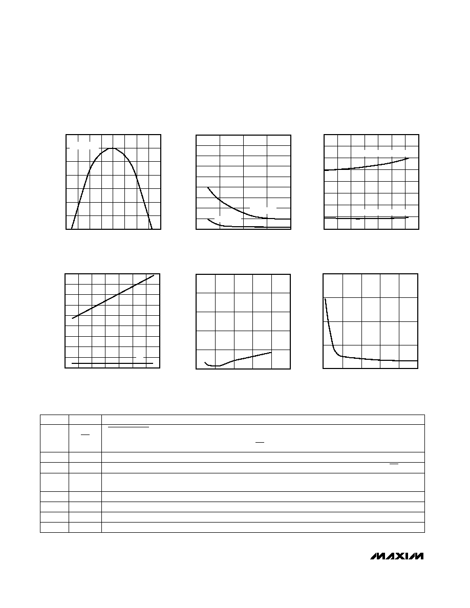
__________________________________________Typical Operating Characteristics
-0.30
-0.25
-0.20
-0.15
-0.10
-0.05
0.05
0
ERROR vs. COMMON-MODE
INPUT VOLTAGE (V
IN
LO≠AGND)
MAX132-01
COMMON-MODE VOLTAGE (V)
-3
-2
-1
0
1
2
3
4
-4
ERROR (% OF FSR)
IN HI = IN LO
0
0
0.5
1.5
50Hz/60Hz READ-ZERO OFFSET
vs. VREF
1.5
3.5
MAX132-02
VREF (V)
READ-ZERO OFFSET (% OF FSR)
1.0
2.0
2.5
4.0
1.0
0.5
3.0
2.0
4.5
60Hz MODE
50Hz MODE
0
-40
-20
20
50Hz/60Hz READ-ZERO OFFSET
vs. TEMPERATURE
0.6
1.4
MAX132-03
TEMPERATURE (∞C)
0
40
60
80
100
1.0
1.6
0.4
0.2
1.2
0.8
READ-ZERO OFFSET (% OF FSR)
60Hz MODE, VREF = 545mV
50Hz MODE, VREF = 655mV
-40
0
50
150
SUPPLY CURRENT
vs. CRYSTAL FREQUENCY
20
100
MAX132-04
CRYSTAL FREQUENCY (kHz)
SUPPLY CURRENT (
µ
A)
100
200
250
300
350
60
120
0
-20
80
40
140
V-
V+
0.10
0.08
0.06
0.04
0.02
0
FULL-SCALE ROLLOVER ERROR
vs. VREF
MAX132-05
VREF (V)
0
0.5
1.0
1.5
2.5
2.0
ROLLOVER ERROR (% OF FSA)
0
5
10
15
20
NOISE vs. NUMBER
OF SAMPLES AVERAGED
MAX132-06
NUMBER OF SAMPLES AVERAGED
0
10
20
30
50
40
NOISE (
µ
V
RMS
)
______________________________________________________________Pin Description
Oscillator Output 2 is normally connected to a 32,768Hz crystal. Do not connect with external clock source.
OSC2
5
Serial Clock Input. On SCLK's rising edge, data is shifted into the internal shift register through DIN. On
SCLK's falling edge, data is clocked out of DOUT.
SCLK
4
Serial Data Out, D7 first bit out. Data is clocked out at the falling edge of SCLK. High impedance when CSis high.
DOUT
3
User-programmable output bit 1--programmed through the serial port.
P1
8
User-programmable output bit 0--programmed through the serial port.
P0
7
Oscillator Input 1 is normally connected to a 32,768Hz crystal, or may be connected to an external clock.
OSC1
6
Serial Data In, D7 first bit in. Data is clocked into the register on the rising edge of SCLK.
DIN
2
PIN
CHIP SELECT Input has 3 functions: 1) When low, selects IC for communication; 2) on rising edge, loads
input shift register data into one of the command registers; 3) on falling edge, loads data from one of the
output registers into the output shift register. When CS is high, DOUT is high impedance.
CS
1
FUNCTION
NAME
MAX132
±18-Bit ADC with Serial Interface
_______________________________________________________________________________________
5
MAX132
CREF-
CREF+
1
20
CS
602k
4
SCLK
3
DOUT
2
DIN
11
EOC
7
P0
8
P1
9
P2
10
P3
23
19
22
21
-5V
512mV INPUT
18
17
6
5
15pF
15pF
BUF OUT
INT OUT
INT IN
4.7nF
32,768Hz
REF+
REF-
16
15
AGND
IN LO
14
IN HI
13
12
V-
24
V+
DGND
OSC2
OSC1
0.1
µ
F
120k
100k
40.2k
2.5V
MAX872
+5V
Figure 1. Test and Typical Application Circuit
_________________________________________________Pin Description (continued)
End of Conversion Output goes high at end of conversion.
EOC
11
Positive Supply, nominally +5V
V+
24
User-programmable output bit 3--programmed through the serial port.
P3
10
Negative Reference Capacitor connection
CREF-
20
Positive Reference Capacitor connection
CREF+
19
Positive Reference Input
REF+
18
Negative Reference Input
REF-
17
Analog Ground
AGND
16
Negative Analog Input
IN LO
15
Buffer-Amplifier Output drives the integrator resistor.
BUF OUT
23
User-programmable output bit 2--programmed through the serial port.
P2
9
PIN
Integrator Output. To minimize noise, this pin should drive the capacitor's outside foil (negative end).
INT OUT
22
Integrator Input. Connect the integration capacitor between INT IN and INT OUT.
INT IN
21
FUNCTION
NAME
Positive Analog Input
IN HI
14
Negative Supply, nominally -5V
V-
13
Digital Ground--power-supply return
DGND
12