General Description
The MAX1448 evaluation kit (EV kit) is a fully assembled
and tested circuit board that contains all the components
necessary to evaluate the performance of the MAX1444,
MAX1446, MAX1448, or MAX1449 10-bit analog-to-digital
converters (ADCs). The MAX1444/MAX1446/MAX1448/
MAX1449 ADCs process differential or single-ended ana-
log inputs. The EV kit allows the user to evaluate the
ADCs with both types of signals from one single-ended
analog signal. The digital output produced by the ADCs
can be easily sampled with a user-provided high-speed
logic analyzer or data-acquisition system. The EV kit
comes with the MAX1448 installed. Order free samples of
the MAX1444EHJ, MAX1446EHJ or MAX1449EHJ to eval-
uate these parts. The EV kit operates from a +3V power
supply. It includes circuitry that generates a clock signal
from an AC signal provided by the user.
Features
o Up to 80Msps Sampling Rate
o Low-Voltage, Low-Power Operation
o Single-Ended or Fully Differential Signal Input
Configuration
o Clock-Shaping Circuit
o Fully Assembled and Tested
Evaluates: MAX1444/MAX1446/MAX1448/MAX1449
MAX1448 Evaluation Kit
________________________________________________________________ Maxim Integrated Products
1
19-1799; Rev 1; 7/01
Component List
DESIGNATION
QTY
DESCRIPTION
C1, C2, C4�C8,
C10,C16�C20,
C22, C27,
C33�C39
22
0.1�F, 50V X7R ceramic
capacitors (0805)
Taiyo Yuden UMK212BJ104KG or
equivalent
C3, C9
2
22pF, 200V ceramic capacitors
(0805)
Murata GRM2195C2D220JV01
C11, C21, C24,
C26, C28, C29,
C31, C32
8
2.2�F,10V tantalum capacitors (A)
AVX TAJA225K010 or
Kemet T494A225K010AS
C12�C15
4
10�F, 10V tantalum capacitors ( B)
AVX TAJB106M010 or
Kemet T494B106K010AS
C23, C30
0
Not installed (0805)
C25
1
1000pF, 50V COG ceramic
capacitor (0805)
Murata GRM2195C1H102JA01
J1
1
2
� 20-pin header
JU1, JU2
2
2-pin headers
JU3, JU4
2
3-pin headers
L1, L2
2
Ferrite chip beads (1206)
Fair-Rite Products Corp.
2512069007Y0 or
HiQ Magnetics 436-2600
R1, R39
0
Not installed (0805)
R2, R3,
R13�R23, R35
14
49.9
�1% resistors (0805)
DESIGNATION
QTY
DESCRIPTION
R4, R5, R38
3
24.9
�1% resistors (0805)
R8, R24�R33
11
100
�1% resistors (0805)
R9, R10, R36
3
2k
�1% resistors (0805)
R11
1
6.04k
�1% resistor (0805)
R12, R37
2
4.02k
�1% resistors (0805)
R40
1
10k
�1% resistor (0805)
R41
1
3.9
�5% resistor (0805)
R34
1
5k
potentiometer
T1
1
RF transformer
Mini-Circuits TT1-6-KK81
U1
1
MAX1448EHJ (32-pin TQFP)
U2
1
Dual CMOS differential line
receiver (8-pin SO)
Maxim MAX9113ESA
U3
1
Buffer/driver 3-state output
(48-pin TSSOP)
Texas Instruments
SN74ALVCH16244DGG or
Pericom PI74ALVCH16244A
SINGLE, DIFF,
CLOCK
3
SMA PC-mount connectors
None
4
Shunts (JU1 to JU4)
None
1
MAX1448 PC board
None
1
MAX1448 data sheet
None
1
MAX1448 EV kit data sheet
Ordering Information
PART
TEMP. RANGE
IC PACKAGE
MAX1448EVKIT
0
�C to +70�C
32 TQFP
For pricing, delivery, and ordering information, please contact Maxim/Dallas Direct! at
1-888-629-4642, or visit Maxim's website at www.maxim-ic.com.
Evaluates: MAX1444/MAX1446/MAX1448/MAX1449
MAX1448 Evaluation Kit
2
_______________________________________________________________________________________
Quick Start
Required Equipment
� DC power supplies:
Digital = +3V, 100mA
Analog = +3V, 100mA
� A function generator with low phase noise and low jit-
ter for clock input (e.g., HP 8662A)
� A function generator for analog signal input (e.g.,
HP 8662A)
� A logic analyzer or data-acquisition system (e.g.,
HP 1663EP, HP 16500C)
� An analog bandpass filter (e.g., TTE elliptical func-
tion bandpass filter Q56 series)
� A digital voltmeter
The MAX1448 EV kit is a fully assembled and tested
surface-mount board. Follow the steps below for board
operation. Do not turn on power supplies or enable
function generators until all connections are com-
pleted.
1) Connect one +3V power supply to VAIN1 and
VAIN2. Connect the ground terminal of this supply
to AGND.
2) Connect one +3V power supply to VDIN1 and
VDIN2. Connect the ground terminal of this supply
to DGND.
3) Verify that shunts are not installed in jumpers JU1
(MAX1448 enabled) and JU2 (MAX1448 output
enabled).
4) Connect the clock function generator to the CLOCK
SMA connector.
5) Connect the output of the analog signal function
generator to the input of the bandpass filter.
6) To evaluate differential analog signals, verify that
shunts are installed on pins 1 and 2 of jumpers JU3
and JU4. Connect the output of the bandpass filter
to the DIFF SMA connector. For single-ended ana-
log signal evaluation, verify that shunts are installed
on pins 2 and 3 of jumpers JU3 and JU4, and con-
nect the output of the bandpass filter to the SINGLE
SMA connector.
7) Connect the logic analyzer to the square pin header
(J1).
8) Turn on both power supplies.
9) With a voltmeter, verify that +1.20V is measured
across test points TP4 and TP5. If the voltage is not
+1.20V, adjust potentiometer R34 until +1.20V is
obtained.
10) Enable the function generators. Set the clock func-
tion generator to 2.4V
P-P
and frequency (f
CLK
)
80MHz. Set the analog signal function generator to
2V
P-P
and desired frequency. The two function gen-
erators should be phase locked to each other.
11) Set the logic analyzer to latch data on the clock's
rising edge.
12) Enable the logic analyzer.
13) Collect data using the logic analyzer.
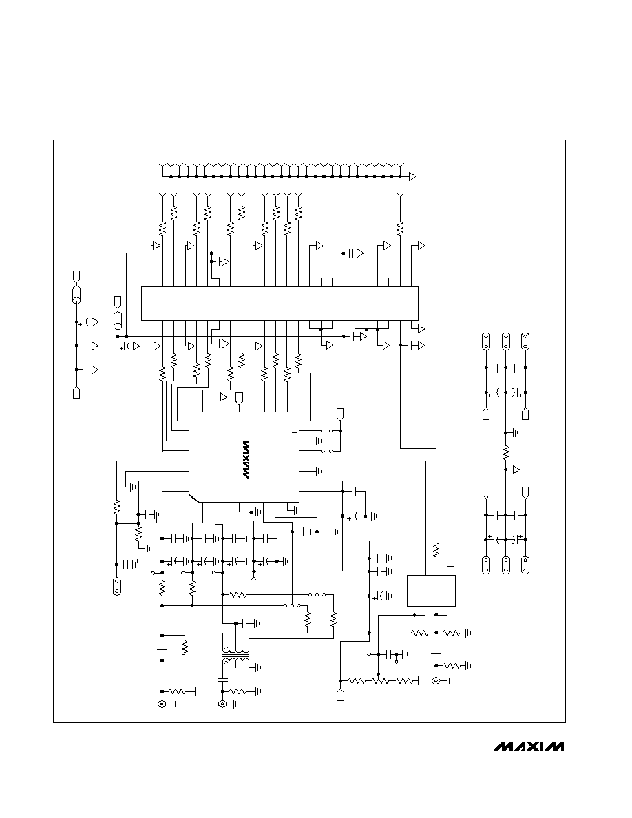
Detailed Description
The MAX1448 EV kit is a fully assembled and tested cir-
cuit board that contains all the components necessary
to evaluate the performance of the MAX1449, MAX1448,
MAX1446, or MAX1444 10-bit ADC at a maximum clock
frequency (f
CLK
) of 80MHz. These ADCs can process
differential or single-ended analog inputs. With the prop-
er board configuration, the user can evaluate the ADC
with both types of signals by supplying only one single-
ended analog signal to the EV kit.
The EV kit's PC board is designed as a four-layer board
to optimize the performance of the MAX1448. Separate
analog and digital power planes minimize noise cou-
pling between analog and digital signals. For simple
operation, the EV kit is specified to have +3V power
Component Suppliers
Part Selection Table
Note: Please indicate that you are using the MAX1448,
MAX1444, MAX1446, or MAX1449 when contacting these
component suppliers.
SUPPLIER
PHONE
FAX
843-448-1943
843-448-9411
AVX
Fair-Rite Products
888-324-7748
888-337-7483
864-963-6322
718-934-7092
847-925-0899
214-480-7800
972-644-5580
800-348-2496
718-934-4500
864-963-6300
Kemet
Mini-Circuits
Taiyo Yuden
Texas Instruments
PART
SPEED (Msps)
MAX1444EHJ
40
MAX1446EHJ
60
MAX1448EHJ
80
MAX1449EHJ
105
770-436-3030
770-436-1300
Murata
408-435-1100
800-435-2336
Pericom
supplies applied to analog and digital power planes.
However, the digital supply can be operated down to
+1.7V without compromising the board's performance.
The logic analyzer's threshold should be adjusted
accordingly.
Access to the output is provided through connector J1.
The 40-pin connector can easily interface directly to a
user-provided logic analyzer or data-acquisition system.
Power Supplies
The MAX1448 EV kit requires separate analog and digi-
tal power supplies for best performance. A +3V power
supply is used to power the analog portion of the
MAX1449/MAX1448/MAX1446/MAX1444 ADC and
the clock signal circuit. The MAX1449/MAX1448/
MAX1446/MAX1444 analog supply voltage has a range
of +2.7V to +3.3V; however, +3V must be supplied to
the EV kit (VAIN1, VAIN2) to meet the minimum input
voltage supply to the clock signal generator. A separate
+3.0V power supply is used to power the digital portion
(VDIN1, VDIN2) of the MAX1448 ADC and the buffer/dri-
ver, but it will operate with a voltage supply as low as
+1.7V and as high as +3.3V. Enhanced dynamic perfor-
mance can be achieved when the digital supply voltage
is lower than the analog supply voltage.
Clock
An on-board clock-shaping circuit generates a clock sig-
nal from an AC sine-wave signal applied to the CLOCK
SMA connector. The signal should not exceed 2.6V
P-P
.
The typical clock frequency should be 80MHz or less.
The frequency of the sinusoidal input signal determines
the sampling frequency of the ADC. A DS90LV028A dif-
ferential line receiver processes the input signal to pro-
duce the CMOS clock signal. The signal's duty cycle can
be adjusted with potentiometer R34. A clock signal with a
50% duty cycle can be achieved by adjusting R34 until
+1.2V is produced across test points TP4 and TP5 at +3V
analog voltage supply (40% of the analog power supply).
Input Signal
The MAX1448 ADC is able to process differential or sin-
gle-ended analog input signals. The EV kit requires only
one single-ended analog input signal provided by the
user. During single-ended signal operation, the signal is
applied directly to the ADC, and in differential signal
operation, an on-board transformer takes the single-
ended analog signal and generates a differential analog
signal at the ADC's differential input pins. For single-
ended or differential signal board operation, see Table 1
for jumper configuration.
Note: When a differential signal is applied to the ADC,
its positive and negative input pins each receive half of
the input signal supplied at SMA connector DIFF cen-
tered at (VAIN1) / 2.
MAX1448 Enable/Shutdown
The MAX1448 EV kit features jumpers to enable and dis-
able the MAX1448 (JU1) or its digital outputs (JU2). See
Table 1 for jumper settings.
External Voltage Reference
The MAX1448 ADC requires an input voltage reference
at pin 31 (REFIN) to set the full-scale analog signal volt-
age input. The ADC also has a stable on-chip voltage
reference of +2.048V that can be accessed at REFOUT.
The EV kit was designed to use the on-chip voltage ref-
erence by connecting REFIN to REFOUT through resis-
tor R40. The user can externally adjust the reference
level, and hence the full-scale range, by installing a
resistor at R39. The adjusted reference level can be cal-
culated by applying the following equation;
V
REFIN
= (R39 / (R40 + R39)) x V
REFOUT
where R39 is the value of the resistor installed, R40 is a
10k
resistor, and V
REFOUT
is +2.048V. Alternatively,
the user can also apply a stable, low-noise, external ref-
erence voltage directly at the REFIN pad to set the full
scale.
Evaluates: MAX1444/MAX1446/MAX1448/MAX1449
MAX1448 Evaluation Kit
_______________________________________________________________________________________
3
Table 1. MAX1448 EV Kit Jumper Selection
JUMPER
SHUNT STATUS
PIN CONNECTION
EV KIT OPERATION
CLOSED
PD connected to VDDUT
MAX1448 is disabled (powered down)
JU1
OPEN
PD connected internally to GND
MAX1448 is enabled
CLOSED
OE connected to VDDUT
MAX1448 digital outputs are disabled
JU2
OPEN
OE connected internally to GND
MAX1448 digital outputs are enabled
1 and 2
IN+ and IN- pins connected to SMA
connector DIFF
Analog input signal is coupled into the
ADC as a differential input
JU3, JU4
2 and 3
IN+ pin connected to SMA connector
SINGLE and IN- pin connected to COM
pin
Analog input signal is coupled into the
ADC as a single-ended input
Evaluates: MAX1444/MAX1446/MAX1448/MAX1449
MAX1448 Evaluation Kit
4
_______________________________________________________________________________________
32
28
29
30
31
25
26
27
REFIN
GND
REFOUT
D0
REFP
D1
D2
D3
10
13
15
14
16
11
12
9
V
DD
GND
V
DD
PD
CLK
OE
D9
GND
17
18
19
20
21
22
23
OGND
24
D4
T.P.
OV
DD
OVDD
VADUT
VA
VD
VA
VDDUT
VADUT
VDDUT
OVDD
D5
D6
D7
D8
GND
NOTE:
ALL RESISTORS ARE 0805 1% UNLESS OTHERWISE NOTED.
U2
MAX9113
U1
U3
SN74ALVCH16244
IN-
IN+
GND
GND
V
DD
COM
2
3
4
5
6
7
8
1
REFN
REFIN
C28
2.2
�
F
10V
C27
0.1
�
F
C36
0.1
�
F
C39
0.1
�
F
C20
0.1
�
F
C21
2.2
�
F
10V
C31
2.2
�
F
10V
C37
0.1
�
F
C35
0.1
�
F
C38
0.1
�
F
C9
22pF
C3
22pF
C12
10
�
F
10V
C15
10
�
F
10V
C34
0.1
�
F
C30
OPEN
C17
0.1
�
F
C16
0.1
�
F
C6
0.1
�
F
RIN1-
RIN2-
RIN1+
RIN2+
V
CC
ROUT1
ROUT2
GND
24
J1-1
J1-3
J1-5
J1-7
J1-9
J1-11
J1-13
J1-15
J1-17
J1-19
J1-21
23
22
21
20
19
18
17
16
15
25
L2
L1
26
27
28
29
30
31
32
33
34
14
13
12
11
10
9
8
7
6
5
35
36
37
38
39
40
41
42
43
44
45
46
4
3
47
48
2
1
4DE
R23, 49.9
R22, 49.9
R33, 100
R32, 100
R39
OPEN
R9
2k
TP1
TP2
TP3
R10
2k
R1
OPEN
T1
1
1
2
2
3
3
1
1
1
2
2
4
2
3
3
8
6
7
5
3
6
5
4
R40
10k
R31, 100
R30, 100
R29, 100
R28, 100
R27, 100
R26, 100
R25, 100
JU2
JU1
R24, 100
R5
24.9
JU3
JU4
R4
24.9
CLOCK
R8, 100
VDIN1
DGND
VDIN2
VDIN1
DGND
VDIN2
R41
3.9
TP4
TP5
R19, 49.9
R18, 49.9
R17, 49.9
R16, 49.9
R15, 49.9
R14, 49.9
R13, 49.9
R21, 49.9
R20, 49.9
3DE
4Y4
4Y3
GND
4Y2
4Y1
V
CC
3Y4
3Y3
GND
3Y2
3Y1
2Y4
2Y3
GND
2Y2
2Y1
V
CC
1Y4
1Y3
GND
1Y2
1Y1
1DE
4A2
GND
4A3
4A4
3A3
3A4
V
CC
4A1
3A2
GND
GND
2A3
2A4
3A1
1A4
V
CC
2A1
2A2
GND
1A3
1A1
1A2
2DE
VDDUT
VD
C29
2.2
�
F
10V
C10
0.1
�
F
C1
0.1
�
F
C2
0.1
�
F
C22
0.1
�
F
C4
0.1
�
F
C33
0.1
�
F
C19
0.1
�
F
C25
1000pF
C32
2.2
�
F
10V
C14
10
�
F
10V
C18
0.1
�
F
C13
10
�
F
10V
SINGLE
DIFF
R38
24.9
R2
49.9
R3
49.9
R37
4.02k
R11
6.04k
R12
4.02k
R35
49.9
R34
5k
R36
2k
C5
0.1
�
F
C26
2.2
�
F
10V
C7
0.1
�
F
C8
0.1
�
F
C23
OPEN
C24
2.2
�
F
10V
C11
2.2
�
F
10V
J1-2
J1-4
J1-6
J1-8
J1-10
J1-12
J1-14
J1-16
J1-18
J1-20
J1-22
J1-23
J1-24
J1-25
J1-26
J1-27
J1-28
J1-29
J1-30
J1-31
J1-32
J1-33
J1-34
J1-35
J1-36
J1-37
J1-38
J1-39
J1-40
MAX1448
Figure 1. MAX1448 EV Kit Schematic
Output Buffer/Driver
The SN74ALVCH16244 buffer/driver buffers the
MAX1448's digital output, which produces straight offset
binary data. The buffer is able to drive capacitive loads,
which may be present at the logic analyzer connection,
without compromising the digital output signal. The out-
puts of the buffer are connected to a 40-pin header (J1)
located on the right side of the EV kit where the user can
connect a logic analyzer or data-acquisition system.
Evaluates: MAX1444/MAX1446/MAX1448/MAX1449
MAX1448 Evaluation Kit
_______________________________________________________________________________________
5
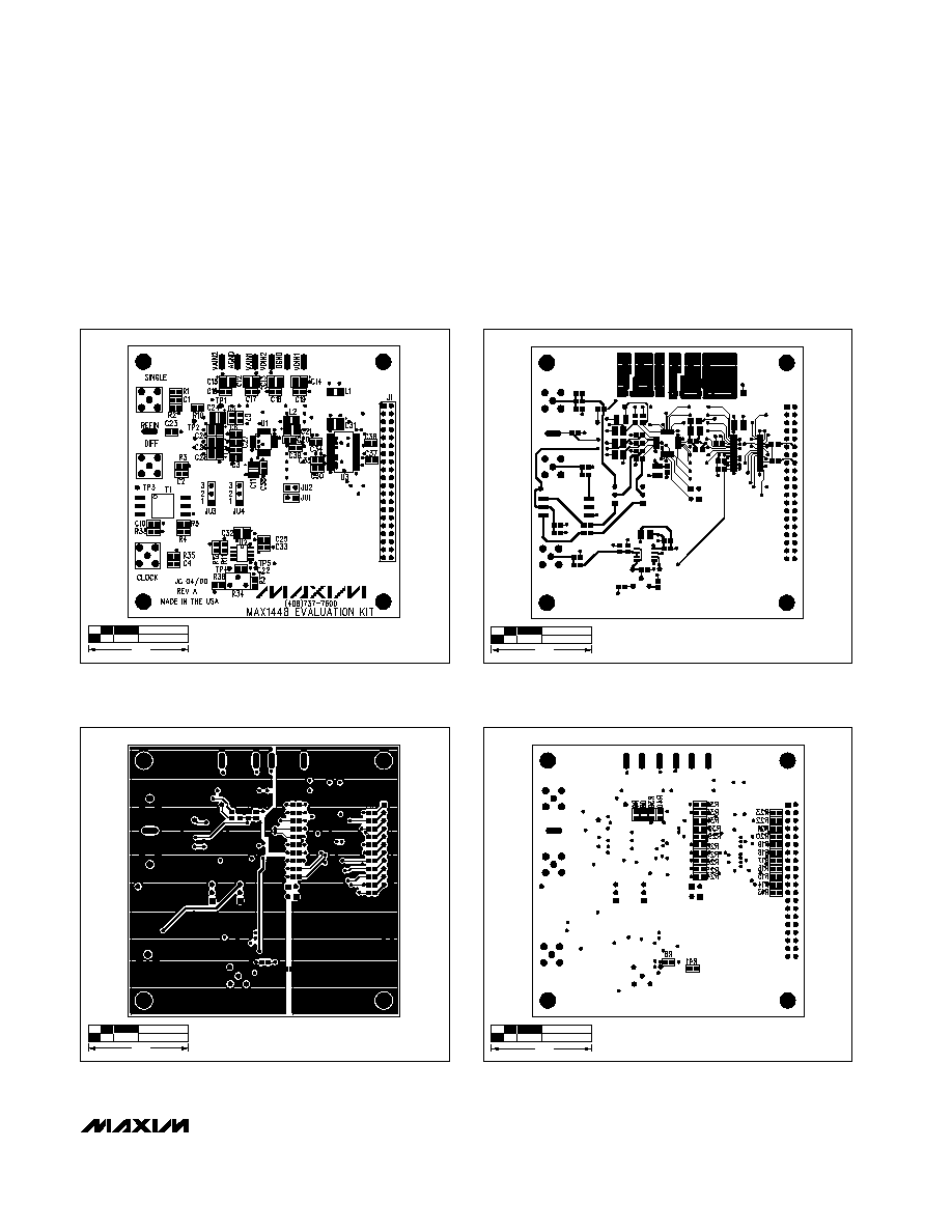
Figure 2. MAX1448EV Kit Component Placement Guide--
Component Side
Figure 3. MAX1448EV Kit PC Board Layout--Component Side
Figure 4. MAX1448EV Kit PC Board Layout--Solder Side
Figure 5. MAX1448EV Kit Component Placement Guide--
Solder Side
1.0"
1.0"
1.0"
1.0"