 | –≠–ª–µ–∫—Ç—Ä–æ–Ω–Ω—ã–π –∫–æ–º–ø–æ–Ω–µ–Ω—Ç: MAX1446 | –°–∫–∞—á–∞—Ç—å:  PDF PDF  ZIP ZIP |

General Description
The MAX1446 10-bit, 3V analog-to-digital converter
(ADC) features a fully differential input, a pipelined 10-
stage ADC architecture with digital error correction and
wideband track and hold (T/H) incorporating a fully dif-
ferential signal path. This ADC is optimized for low-
power, high dynamic performance applications in
imaging and digital communications. The MAX1446
operates from a single 2.7V to 3.6V supply, consuming
only 90mW while delivering a 59.5dB signal-to-noise
ratio (SNR) at a 20MHz input frequency. The fully differ-
ential input stage has a 400MHz, -3dB bandwidth and
may be operated with single-ended inputs. In addition
to low operating power, the MAX1446 features a 5µA
power-down mode for idle periods.
An internal 2.048V precision bandgap reference is used
to set the ADC full-scale range. A flexible reference
structure allows the user to supply a buffered, direct or
externally derived reference for applications requiring
increased accuracy or a different input voltage range.
Lower and higher speed, pin-compatible versions of
the MAX1446 are also available. Refer to the MAX1444
data sheet for a 40Msps version and the MAX1448 data
sheet for a 80Msps version.
The MAX1446 has parallel, offset binary, three-state
outputs that can be operated from 1.7V to 3.3V to allow
flexible interfacing. The device is available in a 5x5mm,
32-pin TQFP package and is specified over the extended
industrial (-40∞C to +85∞C) temperature range.
________________________Applications
Ultrasound Imaging
CCD Imaging
Baseband and IF Digitization
Digital Set-Top Boxes
Video Digitizing Applications
Features
o Single 3.0V Operation
o Excellent Dynamic Performance
59.5dB SNR at f
IN
= 20MHz
73dB SFDR at f
IN
= 20MHz
o Low Power:
30mA (Normal Operation)
5µA (Shutdown Mode)
o Fully Differential Analog Input
o Wide 2Vp-p Differential Input Voltage Range
o 400MHz -3dB Input Bandwidth
o On-Chip 2.048V Precision Bandgap Reference
o CMOS-Compatible Three-State Outputs
o 32-Pin TQFP Package
MAX1446
10-Bit, 60Msps, 3.0V, Low-Power
ADC with Internal Reference
________________________________________________________________ Maxim Integrated Products
1
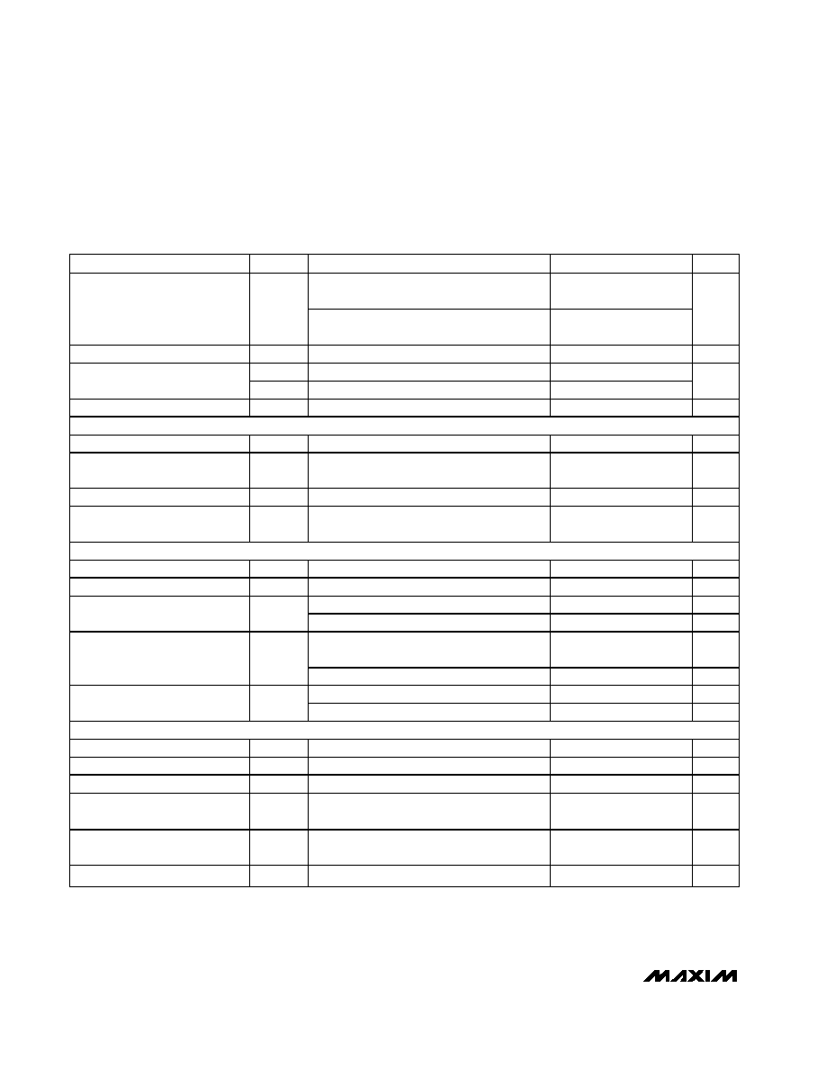
CLK
IN+
CONTROL
10
PIPELINE ADC
REF SYSTEM +
BIAS
OUTPUT
DRIVERS
D
E
C
REF
REFIN
REFOUT
REFP COM REFN
OE
V
DD
GND
OV
DD
OGND
D9≠D0
IN-
PD
T/H
MAX1446
Functional Diagram
19-1729; Rev 1; 7/03
EVALUATION KIT
AVAILABLE
Ordering Information
PART
TEMP RANGE
PIN-PACKAGE
MAX1446EHJ
-40
∞C to +85∞C
32 TQFP
For pricing, delivery, and ordering information, please contact Maxim/Dallas Direct! at
1-888-629-4642, or visit Maxim's website at www.maxim-ic.com.

MAX1446
10-Bit, 60Msps, 3.0V, Low-Power
ADC with Internal Reference
2
_______________________________________________________________________________________
ABSOLUTE MAXIMUM RATINGS
ELECTRICAL CHARACTERISTICS
(V
DD
= 3.0V, OV
DD
= 2.7V; 0.1µF and 1.0µF capacitors from REFP, REFN, and COM to GND; V
REFIN
= 2.048V, REFOUT connected
to REFIN through a 10k
resistor, V
IN
= 2Vp-p (differential with respect to COM), C
L
10pF at digital outputs, f
CLK
= 62.5MHz
(50% duty cycle), T
A
= T
MIN
to T
MAX
, unless otherwise noted.
+25∞C guaranteed by production test, <+25∞C guaranteed by design
and characterization.Typical values are at T
A
= +25
∞C.)
Stresses beyond those listed under "Absolute Maximum Ratings" may cause permanent damage to the device. These are stress ratings only, and functional
operation of the device at these or any other conditions beyond those indicated in the operational sections of the specifications is not implied. Exposure to
absolute maximum rating conditions for extended periods may affect device reliability.
V
DD
, OV
DD
to GND ...............................................-0.3V to +3.6V
OGND to GND.......................................................-0.3V to +0.3V
IN+, IN- to GND........................................................-0.3V to V
DD
REFIN, REFOUT, REFP,
REFN, and COM to GND.........................-0.3V to (V
DD
+ 0.3V)
OE, PD, CLK to GND..................................-0.3V to (V
DD
+ 0.3V)
D9≠D0 to GND.........................................-0.3V to (OV
DD
+ 0.3V)
Continuous Power Dissipation (T
A
= +70
∞C)
32-Pin TQFP (derate 11.1mW/
∞C above +70∞C)...........889mW
Operating Temperature Range ..........................-40
∞C to +85∞C
Storage Temperature Range ............................-60
∞C to +150∞C
Lead Temperature (soldering, 10s) .................................+300
∞C
PARAMETER
SYMBOL
CONDITIONS
MIN
TYP
MAX
UNITS
DC ACCURACY
Resolution
10
Bits
Integral Nonlinearity
INL
f
IN
= 7.492MHz, T
A
+25∞C
±0.6
±1.9
LSB
Differential Nonlinearity
DNL
No missing codes, f
IN
= 7.492MHz
±0.4
±1.0
LSB
Offset Error
-1.6
<
±0.1
±1.9
% FS
Gain Error
0
±2.0
% FS
ANALOG INPUT
Input Differential Range
V
DIFF
Differential or single-ended inputs
±1.0
V
Common-Mode Voltage Range
V
COM
V
DD
/2
± 0.5
V
Input Resistance
R
IN
Switched capacitor load
33
k
Input Capacitance
C
IN
5
pF
CONVERSION RATE
Maximum Clock Frequency
f
CLK
60
MHz
Data Latency
5.5
Cycles
DYNAMIC CHARACTERISTICS (f
CLK
= 62.5MHz, 4096-point FFT)
f
IN
= 7.492MHz
57
59.5
f
IN
= 19.943MHz
56.5
59.5
Signal-to-Noise Ratio
SNR
f
IN
= 39.9MHz (Note 1)
59
dB
f
IN
= 7.492MHz
56.6
59.4
f
IN
= 19.943MHz
56.2
59
Signal-to-Noise Plus Distortion
(up to 5th Harmonic)
SINAD
f
IN
= 39.9MHz (Note 1)
58.5
dB
f
IN
= 7.492MHz
65
74
f
IN
= 19.943MHz
63
73
Spurious-Free Dynamic
Range
SFDR
f
IN
= 39.9MHz (Note 1)
71
dBc

MAX1446
10-Bit, 60Msps, 3.0V, Low-Power
ADC with Internal Reference
_______________________________________________________________________________________
3
ELECTRICAL CHARACTERISTICS (continued)
(V
DD
= 3.0V, OV
DD
= 2.7V; 0.1µF and 1.0µF capacitors from REFP, REFN, and COM to GND; V
REFIN
= 2.048V, REFOUT connected
to REFIN through a 10k
resistor, V
IN
= 2Vp-p (differential with respect to COM), C
L
10pF at digital outputs, f
CLK
= 62.5MHz
(50% duty cycle), T
A
= T
MIN
to T
MAX
, unless otherwise noted.
+25∞C guaranteed by production test, <+25∞C guaranteed by design
and characterization.Typical values are at T
A
= +25
∞C.)
PARAMETER
SYMBOL
CONDITIONS
MIN
TYP
MAX
UNITS
f
IN
= 7.492MHz
-74
f
IN
= 19.943MHz
-73
Third-Harmonic Distortion
HD3
f
IN
= 39.9MHz (Note 1)
-71
dBc
Two-Tone Intermodulation
Distortion
IMD
TT
f
1
= 19MHz at -6.5dBFS,
f
2
= 21MHz at -6.5dBFS (Note 2)
-75
dBc
Third-Order Intermodulation
Distortion
IM3
f
1
= 19MHz at -6.5dBFS
f
2
= 21MHz at -6.5dBFS (Note 2)
-75
dBc
f
IN
= 7.492MHz
-70
-64
f
IN
= 19.943MHz
-70
-63
Total Harmonic Distortion
(First 5 Harmonics)
THD
f
IN
= 39.9MHz (Note 1)
-69
dBc
Small-Signal Bandwidth
Input at -20dBFS, differential inputs
500
MHz
Full-Power Bandwidth
FPBW
Input at -0.5dBFS, differential inputs
400
MHz
Aperture Delay
t
AD
1
ns
Aperture Jitter
t
AJ
2
psrms
Overdrive Recovery Time
For 1.5
◊ full-scale input
2
ns
Differential Gain
±1
%
Differential Phase
±0.25
∞
Output Noise
IN+ = IN- = COM
0.2
LSBrms
INTERNAL REFERENCE
Reference Output Voltage
REFOUT
2.048
±1%
V
Reference Temperature
Coefficient
TC
REF
60
ppm/
∞C
Load Regulation
1.25
mV/mA
EXTERNAL REFERENCE
Positive Reference
REFP
V
REFIN
= 2.048V
2.012
V
Negative Reference
REFN
V
REFIN
= 2.048V
0.988
V
Differential Reference Voltage
V
REF
V
RE FP
- V
RE FN
, V
RE FI N
= 2.048V , T
A
+ 25∞ C 0.98
1.024
1.07
V
REFIN Resistance
R
REFIN
>50
M
D IGIT A L IN PU T S ( C LK, P D ,
OE )
CLK
0.8 x
V
DD
Input High Threshold
V
IH
PD,
OE
0.8 x
OV
D D
V
PARAMETER
SYMBOL
CONDITIONS
MIN
TYP
MAX
UNITS
CLK
0.2 x
V
DD
Input Low Threshold
V
IL
PD,
OE
0.2 x
OV
D D
V
Input Hysteresis
V
HYST
0.1
V
I
IH
V
IH
= V
DD
= OV
DD
±5
Input Leakage
I
IL
V
IL
= 0
±5
µA
Input Capacitance
C
IN
5
pF
DIGITAL OUTPUTS (D9≠D0)
Output Voltage Low
V
OL
I
SINK
= 200µA
0.2
V
Output Voltage High
V
OH
I
SOURCE
= 200µA
OV
DD
-
0.2
V
Three-State Leakage Current
I
LEAK
OE = OV
DD
±10
µA
Three-State Output Capacitance
C
OUT
OE = OV
DD
5
pF
POWER REQUIREMENTS
Analog Supply Voltage
V
DD
2.7
3.0
3.6
V
Output Supply Voltage
OV
DD
C
L
= 10pF
1.7
3.0
3.6
V
Operating, f
IN
= 19.943MHz at -0.5dBFS
30
37
mA
Analog Supply Current
I
VDD
Shutdown, clock idle, PD =
OE = OV
DD
4
15
µA
Operating, C
L
= 15pF, f
IN
= 19.943MHz at
-0.5dBFS
7
mA
Output Supply Current
I
OVDD
Shutdown, clock idle, PD =
OE = OV
DD
1
20
µA
Offset
± 0.1
mV/V
Power-Supply Rejection
PSRR
Gain
± 0.1
%/V
TIMING CHARACTERISTICS
CLK Rise to Output Data Valid
t
DO
Figure 5 (Note 3)
5
8
ns
OE Fall to Output Enable
t
ENABLE
Figure 5
10
ns
OE Rise to Output Disable
t
DISABLE
Figure 5
1.5
ns
CLK Pulse Width High
t
CH
Figure 6, clock period 16ns
8.3
± 2.5
ns
CLK Pulse Width Low
t
CL
Figure 6, clock period 16ns
8.3
± 2.5
ns
Wake-Up Time
t
WAKE
(Note 4)
1.5
µs
Note 1: SNR, SINAD, THD, SFDR, and HD3 are based on an analog input voltage of -0.5dBFS referenced to a +1.024V full-scale
input voltage range.
Note 2: Intermodulation distortion is the total power of the intermodulation products relative to the individual carrier. This number is
6dB better, if referenced to the two-tone envelope.
Note 3: Digital outputs settle to V
IH
, V
IL
.
Note 4: With R
EFIN
driven externally, REFP, COM, and REFN are left floating while powered down.
MAX1446
10-Bit, 60Msps, 3.0V, Low-Power
ADC with Internal Reference
4
_______________________________________________________________________________________
ELECTRICAL CHARACTERISTICS (continued)
(V
DD
= 3.0V, OV
DD
= 2.7V; 0.1µF and 1.0µF capacitors from REFP, REFN, and COM to GND; V
REFIN
= 2.048V, REFOUT connected
to REFIN through a 10k
resistor, V
IN
= 2Vp-p (differential with respect to COM), C
L
10pF at digital outputs, f
CLK
= 62.5MHz
(50% duty cycle), T
A
= T
MIN
to T
MAX
, unless otherwise noted.
+25∞C guaranteed by production test, <+25∞C guaranteed by design
and characterization.Typical values are at T
A
= +25
∞C.)
MAX1446
10-Bit, 60Msps, 3.0V, Low-Power
ADC with Internal Reference
_______________________________________________________________________________________
5
-100
-70
-80
-90
-50
-60
-10
-20
-30
-40
0
0
5
10
15
20
25
30
35
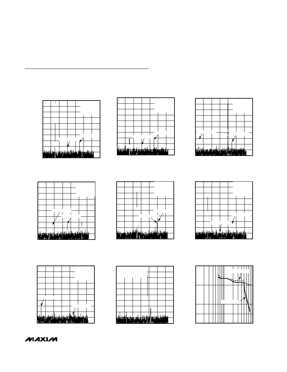
FFT PLOT
f
IN
= 7.5MHz, 8192-POINT FFT,
DIFFERENTIAL INPUT
ANALOG INPUT FREQUENCY (MHz)
AMPLITUDE (dB)
SFDR = 72.2dB
SNR = 60.1dB
THD = -71.5dB
SINAD = 59.8dB
3RD HARMONIC
2ND HARMONIC
MAX1446 toc01
-100
-70
-80
-90
-50
-60
-10
-20
-30
-40
0
0
5
10
15
20
25
30
35
FFT PLOT
(f
IN
= 7.5MHz, 8192-POINT FFT,
DIFFERENTIAL INPUT)
ANALOG INPUT FREQUENCY (MHz)
AMPLITUDE (dB)
SFDR = 72.2dBc
SNR = 60.1dB
THD = -71.5dBc
SINAD = 59.8dB
3RD HARMONIC
2ND HARMONIC
-100
-70
-80
-90
-50
-60
-10
-20
-30
-40
0
0
5
10
15
20
25
30
35
FFT PLOT
(f
IN
= 20MHz, 8192-POINT FFT,
DIFFERENTIAL INPUT)
MAX1446 toc03
ANALOG INPUT FREQUENCY (MHz)
AMPLITUDE (dB)
SINAD = 59.3dB
SNR = 59.6dB
THD = -70.7dBc
SFDR = 72.2dBc
3RD HARMONIC
2ND HARMONIC
-100
-70
-80
-90
-50
-60
-10
-20
-30
-40
0
0
5
10
15
20
25
30
35
FFT PLOT
(f
IN
= 26.8MHz, 8192-POINT FFT,
DIFFERENTIAL INPUT)
MAX1446 toc04
ANALOG INPUT FREQUENCY (MHz)
AMPLITUDE (dB)
SINAD = 59.0dB
SNR = 59.4dB
THD = -70.5dBc
SFDR = 72.9dBc
3RD HARMONIC
2ND HARMONIC
-100
-70
-80
-90
-50
-60
-10
-20
-30
-40
0
0
5
10
15
20
25
30
35
FFT PLOT
(f
IN
= 50MHz, 8192-POINT FFT,
DIFFERENTIAL INPUT)
MAX1446 toc05
ANALOG INPUT FREQUENCY (MHz)
AMPLITUDE (dB)
SFDR = 70dBc
SNR = 59.1dB
THD = -67.1dBc
SINAD = 58.5dB
3RD HARMONIC
2ND HARMONIC
-100
-70
-80
-90
-50
-60
-10
-20
-30
-40
0
0
5
10
15
20
25
30
35
FFT PLOT
(f
IN
= 7.5MHz, 8192-POINT FFT,
SINGLE-ENDED INPUT)
MAX1446 toc06
ANALOG INPUT FREQUENCY (MHz)
AMPLITUDE (dB)
SINAD = 59.5dB
SNR = 59.7dB
THD = -73.0dBc
SFDR = 73.6dBc
3RD HARMONIC
2ND HARMONIC
-100
-70
-80
-90
-50
-60
-10
-20
-30
-40
0
0
5
10
15
20
25
30
35
FFT PLOT
(f
IN
= 20MHz, 8192-POINT FFT,
SINGLE-ENDED INPUT)
MAX1446 toc07
ANALOG INPUT FREQUENCY (MHz)
AMPLITUDE (dB)
SINAD = 59.2dB
SNR = 59.5dB
THD = -70.7dBc
SFDR = 71.1dBc
3RD HARMONIC
2ND HARMONIC
Typical Operating Characteristics
(V
DD
= 3.0V, OV
DD
= 2.7V, internal reference, differential input at -0.5dBFS, f
CLK
= 62.35MHz, C
L
10pF, T
A
= +25∞C,
unless otherwise noted.)
-100
-70
-80
-90
-50
-60
-10
-20
-30
-40
0
0
5
10
15
20
25
30
35
TWO-TONE INTERMODULATION
(8192-POINT IMD,
DIFFERENTIAL INPUT)
MAX1446 toc10
ANALOG INPUT FREQUENCY (MHz)
AMPLITUDE (dB)
f1 = 19MHz AT -6.5dBFS
f2 = 21MHz AT -6.5dBFS
3RD IMD = -76dBc
1
10
100
MAX1446 toc11
ANALOG INPUT FREQUENCY (MHz)
SINAD (dBc)
DIFFERENTIAL
SINGLE ENDED
SPURIOUS-FREE DYNAMIC RANGE
vs. ANALOG INPUT FREQUENCY
80
50
55
60
65
70
75