 | –≠–ª–µ–∫—Ç—Ä–æ–Ω–Ω—ã–π –∫–æ–º–ø–æ–Ω–µ–Ω—Ç: MAX1510 | –°–∫–∞—á–∞—Ç—å:  PDF PDF  ZIP ZIP |
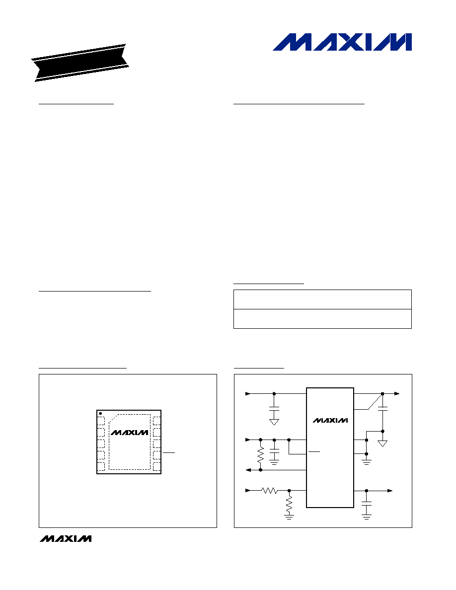
General Description
The MAX1510 DDR linear regulator sources and sinks up
to 3A peak (typ) using internal n-channel MOSFETs. This
linear regulator delivers an accurate 0.5V to 1.5V output
from a low-voltage power input (V
IN
= 1.1V to 3.6V). The
MAX1510 uses a separate 3.3V bias supply to power the
control circuitry and drive the internal n-channel
MOSFETs.
The MAX1510 provides current and thermal limits to
prevent damage to the linear regulator. Additionally,
the MAX1510 generates a power-good (PGOOD) signal
to indicate that the output is in regulation. During start-
up, PGOOD remains low until the output is in regulation
for 2ms (typ). The internal soft-start limits the input
surge current.
The MAX1510 powers the active-DDR termination bus
that requires a tracking input reference. The MAX1510
can also be used in low-power chipsets and graphics
processor cores that require dynamically adjustable
output voltages. The MAX1510 is available in a 10-pin
3mm x 3mm thin DFN package.
Applications
Notebook/Desktop Computers
DDR Memory Termination
Active Termination Buses
Graphics Processor Core Supplies
Chipset/RAM Supplies as Low as 0.5V
Features
o Internal Power MOSFETs with Current Limit (3A typ)
o Fast Load-Transient Response
o External Reference Input with Reference
Output Buffer
o 1.1V to 3.6V Power Input
o ±15mV (max) Load-Regulation Error
o Thermal Fault Protection
o Shutdown Input
o Power-Good Window Comparator with 2ms
(typ) Delay
o Small, Low-Profile 10-Pin 3mm x 3mm TDFN
Package
o Ceramic or Polymer Output Capacitors
MAX1510
Low-Voltage DDR Linear Regulator
________________________________________________________________ Maxim Integrated Products
1
Ordering Information
OUT
IN
OUTS
AGND
PGND
V
OUT
= V
TT
V
IN
(1.1V TO 3.6V)
V
BIAS
(2.7V TO 3.6V)
V
DDQ
(2.5V OR 1.8V)
V
REFOUT
= V
TTR
REFOUT
MAX1510
V
CC
PGOOD
SHDN
REFIN
Typical Operating Circuit
19-3279; Rev 0; 5/04
For pricing, delivery, and ordering information, please contact Maxim/Dallas Direct! at
1-888-629-4642, or visit Maxim's website at www.maxim-ic.com.
EVALUATION KIT
AVAILABLE
PART
TEMP RANGE
PIN-
PACKAGE
TOP
MARK
MAX1510ETB
-40
∞C to +85∞C
10 TDFN
(3mm x 3mm)
ABD
SHDN
OUTS
PGOOD
2
3
9
8
OUT
PGND
AGND
REFIN
V
CC
TDFN
3mm x 3mm
TOP VIEW
4
5
7
6
1
IN
REFOUT
MAX1510
10
Pin Configuration

MAX1510
Low-Voltage DDR Linear Regulator
2
_______________________________________________________________________________________
ABSOLUTE MAXIMUM RATINGS
ELECTRICAL CHARACTERISTICS
(V
IN
= 1.8V, V
CC
= 3.3V, V
REFIN
= V
OUTS
= 1.25V,
SHDN = V
CC
, circuit of Figure 1, T
A
= -40
∞C to +85∞C, unless otherwise noted.
Typical values are at T
A
= +25
∞C.) (Note 1)
Stresses beyond those listed under "Absolute Maximum Ratings" may cause permanent damage to the device. These are stress ratings only, and functional
operation of the device at these or any other conditions beyond those indicated in the operational sections of the specifications is not implied. Exposure to
absolute maximum rating conditions for extended periods may affect device reliability.
IN to PGND...............................................................-0.3V to +4V
OUT to PGND ..............................................-0.3V to (V
IN
+ 0.3V)
OUTS to AGND ............................................-0.3V to (V
IN
+ 0.3V)
V
CC
to AGND............................................................-0.3V to +4V
REFIN, REFOUT,
SHDN, PGOOD to AGND ..-0.3V to (V
CC
+ 0.3V)
PGND to AGND .....................................................-0.3V to +0.3V
REFOUT Short Circuit to AGND .................................Continuous
OUT Continuous RMS Current: 100s ..................................
±1.6A
1s......................................±2.5A
Continuous Power Dissipation (T
A
= +70∞C)
10-Pin 3mm x 3mm Thin DFN
(derated 24.4mW/
∞C above +70∞C)...........................1951mW
Operating Temperature Range
MAX1510ETB...................................................-40∞C to +85∞C
Junction Temperature ......................................................+150∞C
Storage Temperature Range .............................-65∞C to +150∞C
Lead Temperature (soldering, 10s) .................................+300∞C
PARAMETER
SYMBOL
CONDITIONS
MIN
TYP
MAX
UNITS
V
IN
Power input
1.1
3.6
Input Voltage Range
V
CC
Bias supply
2.7
3.6
V
Quiescent Supply Current (V
CC
)
I
CC
Load = 0, V
REFIN
> 0.45V
0.7
1.3
mA
SHDN = GND, V
REFIN
> 0.45V
350
600
µA
Shutdown Supply Current (V
CC
)
I
CC(SHDN)
SHDN = GND, REFIN = GND
50
100
µA
Quiescent Supply Current (V
IN
)
I
IN
Load = 0
0.4
10
mA
Shutdown Supply Current (V
IN
)
I
IN(SHDN)
SHDN = GND
0.1
10
µA
T
A
= 25∞C
-4
0
+4
Feedback-Voltage Error
V
OUTS
REFIN to OUTS
I
OUT
=
±200mA
T
A
= -40∞C to +85∞C
-6
+6
mV
Load-Regulation Error
-1A
I
OUT
+1A
-15
+15
mV
Line-Regulation Error
1.4V
V
IN
3.3V, I
OUT
= ±100mA
1
mV
OUTS Input Bias Current
I
OUTS
-1
+1
µA
OUTPUT
Output Adjust Range
0.5
1.5
V
High-side MOSFET (source) (I
OUT
= 0.1A)
0.10
0.25
OUT On-Resistance
Low-side MOSFET (sink) (I
OUT
= -0.1A)
0.10
0.25
Output Current Slew Rate
C
OUT
= 100µF, I
OUT
= 0.1A to 2A
3
A/µs
OUT Power-Supply Rejection
Ratio
PSRR
10Hz < f < 10kHz, I
OUT
= 200mA,
C
OUT
= 100µF
80
dB
OUT to OUTS Resistance
R
OUTS
12
k
Discharge MOSFET On-
Resistance
R
DISCHARGE
SHDN = GND
8
MAX1510
Low-Voltage DDR Linear Regulator
_______________________________________________________________________________________
3
Note 1: Limits are 100% production tested at T
A
= +25
∞C. Limits over the operating temperature range are guaranteed through cor-
relation using statistical-quality-control (SQC) methods.
ELECTRICAL CHARACTERISTICS (continued)
(V
IN
= 1.8V, V
CC
= 3.3V, V
REFIN
= V
OUTS
= 1.25V,
SHDN = V
CC
, circuit of Figure 1, T
A
= -40
∞C to +85∞C, unless otherwise noted.
Typical values are at T
A
= +25
∞C.) (Note 1)
PARAMETER
SYMBOL
CONDITIONS
MIN
TYP
MAX
UNITS
REFERENCE
REFIN Voltage Range
V
REFIN
0.5
1.5
V
REFIN Input Bias Current
I
REFIN
-1
+1
µA
REFIN Undervoltage-Lockout
Voltage
Rising edge, hysteresis = 75mV
0.35
0.45
V
REFOUT Voltage
V
REFOUT
V
CC
= 3.3V, I
REFOUT
= 0
V
REFIN
-0.01
V
REFIN
V
REFIN
+0.01
V
REFOUT Load Regulation
V
REFOUT
I
REFOUT
=
±5mA
-20
+20
mV
FAULT DETECTION
Thermal-Shutdown Threshold
T
SHDN
Rising edge, hysteresis = 15∞C
+165
∞C
V
CC
Undervoltage-Lockout
Threshold
V
UVLO
Rising edge, hysteresis = 100mV
2.45
2.55
2.65
V
IN Undervoltage-Lockout
Threshold
Rising edge, hysteresis = 55mV
0.9
1.1
V
Current-Limit Threshold
I
LIMIT
1.8
3
4.2
A
Soft-Start Current-Limit Time
t
SS
200
µs
INPUTS AND OUTPUTS
PGOOD Lower Trip Threshold
With respect to feedback threshold,
hysteresis = 12mV
-200
-150
-100
mV
PGOOD Upper Trip Threshold
With respect to feedback threshold,
hysteresis = 12mV
100
150
200
mV
PGOOD Propagation Delay
t
PGOOD
OUTS forced 25mV beyond PGOOD trip
threshold
5
10
35
µs
PGOOD Startup Delay
Startup rising edge, OUTS within
±100mV of
the feedback threshold
1
2
3.5
ms
PGOOD Output Low Voltage
I
SINK
= 4mA
0.3
V
PGOOD Leakage Current
I
PGOOD
OUTS = REFIN (PGOOD high impedance),
PGOOD = V
CC
+ 0.3V
1
µA
Logic high
2.0
V
SHDN Logic Input Threshold
Logic low
0.8
V
SHDN Logic Input Current
SHDN = V
CC
or GND
-1
+1
µA
MAX1510
Low-Voltage DDR Linear Regulator
4
_______________________________________________________________________________________
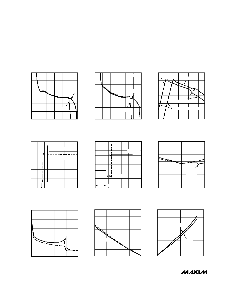
0.84
0.94
0.92
0.90
0.88
0.86
0.96
-3
3
-2
-1
0
1
2
OUTPUT LOAD REGULATION
MAX1510 toc01
I
OUT
(A)
V
OUT
(V)
V
REFIN
= 0.9V
V
IN
= 1.2V
V
IN
= 1.5V
1.200
1.250
1.225
1.275
1.300
-3
3
-2
-1
0
1
2
OUTPUT LOAD REGULATION
MAX1510 toc02
I
OUT
(A)
V
OUT
(V)
V
REFIN
= 1.25V
V
IN
= 1.5V
V
IN
= 1.8V
0
2.5
2.0
1.5
1.0
0.5
3.0
1.0
1.5
2.0
2.5
3.0
MAXIMUM OUTPUT CURRENT
vs. INPUT VOLTAGE
MAX1510 toc03
INPUT VOLTAGE (V)
MAXIMUM OUTPUT CURRENT (A)
DROPOUT VOLTAGE LIMITED
THERMALLY LIMITED
V
OUT
= 1.25V
V
OUT
= 0.9V
BIAS CURRENT (I
CC
)
vs. INPUT VOLTAGE (V
IN
)
MAX1510 toc05
V
IN
(V)
I
IN
(mA)
3.0
2.5
1.5
2.0
1.0
0.5
0.1
0.2
0.3
0.4
0.5
0.6
0.7
0.8
0.9
1.0
0.0
0.0
3.5
V
OUT
= 1.25V
DROPOUT
INPUT UVLO
BIAS CURRENT (I
CC
)
vs. LOAD CURRENT (I
OUT
)
MAX1510 toc06
I
OUT
(A)
I
CC
(mA)
1
0
-1
0.2
0.4
0.6
0.8
1.0
1.2
1.4
0.0
-2
2
V
IN
= 1.5V
V
OUT
= 1.25V
V
OUT
= 0.90V
ENTERING
DROPOUT
POWER GROUND CURRENT (I
PGND
)
vs. SOURCE LOAD CURRENT (I
OUT
)
MAX1510 toc07
I
OUT
(A)
I
PGND
(mA)
1.5
1.0
0.5
0.05
0.10
0.15
0.20
0.25
0.00
0.0
2.0
V
OUT
= 1.25V
V
OUT
= 0.90V
V
IN
= 1.5V
ENTERING
DROPOUT
INPUT CURRENT (I
IN
)
vs. SINK LOAD CURRENT (I
OUT
)
MAX1510 toc08
I
OUT
(A)
I
CC
(mA)
-0.5
-1.0
-1.5
1
2
3
4
5
6
7
0
-2.0
0.0
V
IN
= 1.5V
V
OUT
= 0.90V
V
OUT
= 1.25V
0
0.5
0.4
0.3
0.2
0.1
0.6
0
3.0
0.5
1.0
1.5
2.0
2.5
DROPOUT VOLTAGE
vs. OUTPUT CURRENT
MAX1510 toc09
OUTPUT CURRENT (A)
DROPOUT VOLTAGE (V)
V
OUT
= 1.25V
V
OUT
= 0.9V
Typical Operating Characteristics
(Circuit of Figure 1. T
A
= +25∞C, unless otherwise noted)
INPUT CURRENT (I
IN
)
vs. INPUT VOLTAGE (V
IN
)
MAX1510 toc04
V
IN
(V)
I
IN
(
µ
A)
3.0
2.5
2.0
1.5
1.0
0.5
50
100
150
200
250
0
0.0
3.5
V
OUT
= 1.25V
V
OUT
= 0.90V
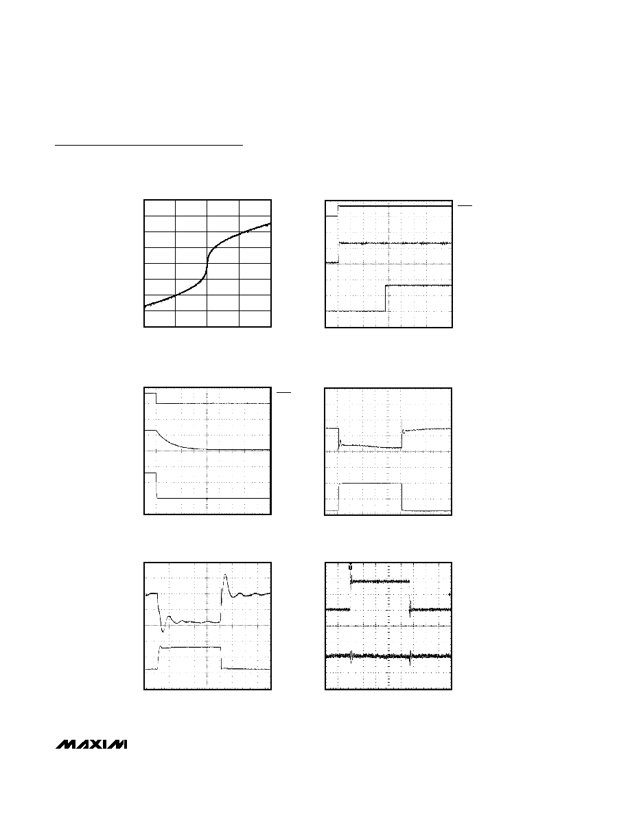
MAX1510
Low-Voltage DDR Linear Regulator
_______________________________________________________________________________________
5
SHUTDOWN WAVEFORM
MAX1510 toc12
100
µs/div
5V
0V
0V
4V
2V
1V
0V
V
OUT
PGOOD
SHDN
R
LOAD
= 100
SOURCE LOAD TRANSIENT
MAX1510 toc13
20.0
µs/div
1A
1mV/div
0A
V
OUT
AC-COUPLED
I
OUT
SOURCE/SINK LOAD TRANSIENT
MAX1510 toc14
4.00
µs/div
+1.5A
5mV/div
-1.5A
V
OUT
AC-COUPLED
I
OUT
LINE TRANSIENT
MAX1510 toc15
40
µs/div
3.3V
0.9V
1.5V
V
IN
(1V/div)
V
OUT
(10mV/div)
AC-COUPLED
I
OUT
= 100mA
Typical Operating Characteristics (continued)
(Circuit of Figure 1. T
A
= +25∞C, unless otherwise noted)
-20
-15
-10
-5
0
5
10
15
20
-10
-5
0
5
10
REFOUT VOLTAGE ERROR
vs. REFOUT LOAD CURRENT
MAX1510 toc10
REFOUT LOAD CURRENT (mA)
REFOUT VOLTAGE ERROR (mV)
STARTUP WAVEFORM
MAX1510 toc11
500
µs/div
5V
0V
0V
4V
0V
1.25V
PGOOD
V
OUT
SHDN