 | –≠–ª–µ–∫—Ç—Ä–æ–Ω–Ω—ã–π –∫–æ–º–ø–æ–Ω–µ–Ω—Ç: MAX1613 | –°–∫–∞—á–∞—Ç—å:  PDF PDF  ZIP ZIP |
General Description
The MAX1612/MAX1613 manage the bridge battery
(sometimes called a hot-swap or auxiliary battery) in
portable systems such as notebook computers. They
feature a step-up DC-DC converter that boosts 2-cell or
3-cell bridge-battery voltages up to the same level as
the main battery. This voltage boosting technique
reduces the number of cells otherwise required for a 6-
cell plus diode-OR bridging scheme, reducing overall
size and cost. Another key feature is a trickle-charge
timer that minimizes battery damage caused by con-
stant charging and eliminates trickle-charge current
drain on the main battery once the bridge battery is
topped off.
These devices contain a highly flexible collection of
independent circuit blocks that can be wired together
in an autonomous stand-alone configuration or used in
conjunction with a microcontroller. In addition to the
boost converter and charge timer, there is a micropow-
er linear regulator (useful for RTC/CMOS backup as
well as for powering a microcontroller) and a high-pre-
cision low-battery detection comparator.
The two devices differ only in the preset linear-regulator
output voltage: +5.0V for the MAX1612 and +3.3V for
the MAX1613. Both devices come in a space-saving
16-pin QSOP package.
Applications
Notebook Computers
Portable Equipment
Backup Battery Applications
Features
o
Reduce Battery Size and Cost
o
Four Key Circuit Blocks
Adjustable Boost DC-DC Converter
NiCd/NiMH Trickle Charger
Always-On Linear Regulator (+28V Input)
Low-Battery Detector
o
Low 18µA Quiescent Current
o
Selectable Charging/Discharging Rates
o
Preset Linear-Regulator Voltage
5V (MAX1612)
3.3V (MAX1613)
o
4V to 28V Main Input Voltage Range
o
Internal Switch Boost Converter
o
Small 16-Pin QSOP Package
MAX1612/MAX1613
Bridge-Battery Backup Controllers
for Notebooks
________________________________________________________________
Maxim Integrated Products
1
16
15
14
13
12
11
10
9
1
2
3
4
5
6
7
8
ISET
LRI
LRO
PGND
CD
CC
GND
LBI
FB
TOP VIEW
MAX1612
MAX1613
QSOP
BBATT
LX
DCMD
LBO
BBON
CCMD
FULL
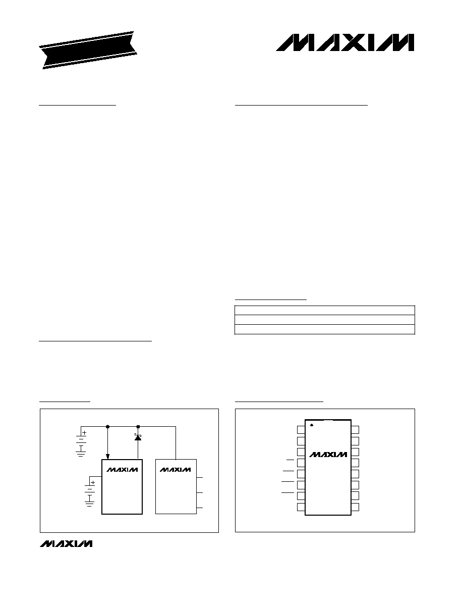
BBATT
LRI
+3.3V
+5V
V+
V
CPU
AUXILIARY
BRIDGE
BATTERY
MAIN BATTERY
OR
WALL
ADAPTER
DC-DC
OUTPUT
APPLICATION
CIRCUIT
DC-DC
CONVERTER
MAX1630
MAX1612
MAX1613
Typical Operating Circuit
19-4785; Rev 0; 11/98
PART
MAX1612
EEE
MAX1613
EEE
-40∞C to +85∞C
-40∞C to +85∞C
TEMP. RANGE
PIN-PACKAGE
16 QSOP
16 QSOP
EVALUATION KIT MANUAL
FOLLOWS DATA SHEET
Pin Configuration
Ordering Information
For free samples & the latest literature: http://www.maxim-ic.com, or phone 1-800-998-8800.
For small orders, phone 1-800-835-8769.
MAX1612/MAX1613
Bridge-Battery Backup Controllers
for Notebooks
2
_______________________________________________________________________________________
ABSOLUTE MAXIMUM RATINGS
ELECTRICAL CHARACTERISTICS
(V
LRI
= V
ISET
= 20V, CCMD = DCMD = BBON = LRO, V
BBATT
= 3V, T
A
= T
MIN
to T
MAX
, unless otherwise noted. Typical values are at
T
A
= +25∞C.) (Note 1)
Stresses beyond those listed under "Absolute Maximum Ratings" may cause permanent damage to the device. These are stress ratings only, and functional
operation of the device at these or any other conditions beyond those indicated in the operational sections of the specifications is not implied. Exposure to
absolute maximum rating conditions for extended periods may affect device reliability.
LRI, ISET to GND....................................................-0.3V to +30V
LX to GND ..............................................................-0.3V to +14V
PGND to GND .......................................................-0.3V to +0.3V
BBATT, LRO, CCMD, DCMD, FULL, BBON,
LBO to GND ..........................................................-0.3V to +6V
CC, CD, LBI, FB to GND...........................-0.3V to (V
LRO
+ 0.3V)
FB, LBI, ISET, and BBATT Current......................................50mA
LRO Output Current ...........................................................50mA
Continuous Power Dissipation (T
A
= +70∞C)
QSOP (derate 8.30mW/∞C above +70∞C) .................... 667mW
Operating Temperature Range
MAX1612/MAX1613EEE ...................................-40∞C to +85∞C
Storage Temperature Range .............................-65∞C to +160∞C
Lead Temperature (soldering, 10sec) ............................ +300∞C
I
SINK
= 1mA
V
LBO
= V
FULL
= 5.5V
V
BBON
2V
V
LBI
= 1.9V
MAX1613
MAX1612
V
ISET
= 28V, V
BBATT
= 0
LRO rising hysteresis = 200mV
CCMD = GND, I
ISET
= 10mA, V
BBATT
= 2V,
%loss = [(I
ISET
- I
BBATT
) / I
ISET
)
∑
100%
V
DCMD
= 0, R
BBON
= 1M
to GND
(boost converter on)
5.7V
V
LRI
28V
(MAX1612)
I
ISET
= 10mA, V
CCMD
= 0, V
BBATT
= 2V
V
ISET
= 0 or 28V, V
BBATT
= 6V
CONDITIONS
LBO, FULL Output Voltage Low
V
0.4
LBO, FULL Output Leakage
Current
µA
1
I
LBO,
I
FULL
nA
0.2
10
I
LBI
LBI Input Current
V
1.955
2
2.045
V
LBTH
LBI Rising Trip Voltage
V
1.76
1.8
1.84
V
LBTL
LBI Falling Trip Voltage
%
0.1
5
Charge-Switch Loss Current
V
0.5
1
1.3
Charge-Switch On Voltage
µA
-5
5
I
BBATT(LEAK
)
BBATT Leakage Current
18
28
I
LRI
4V
V
LRI
28V
(MAX1613)
0
I
LRO
10mA
4
28
V
5.7
28
V
LRI
Linear-Regulator Input Voltage
Range
µA
0.3
5
I
ISET(LEAK
)
ISET Leakage Current
V
2.65
2.97
V
UVLO
Linear-Regulator Output
Undervoltage Lockout
Threshold
V
3.1
3.3
3.5
µA
42
58
Linear-Regulator Quiescent
Current
4.7
5.0
5.3
V
LRO
Linear-Regulator Output Voltage
UNIT
MIN
TYP
MAX
SYMBOL
PARAMETER
Overdrive = 100mV
µs
20
t
PD
LBI Comparator Response Time
BATTERY CHARGER
LOW-BATTERY COMPARATOR

MAX1612/MAX1613
Bridge-Battery Backup Controllers
for Notebooks
_______________________________________________________________________________________
3
Typical Operating Characteristics
(Circuit of Figure 3, T
A
= +25∞C, unless otherwise noted.)
CONDITIONS
UNIT
MIN
TYP
MAX
SYMBOL
PARAMETER
CCMD, DCMD
V
CCMD
= 0, CC = GND
V
DCMD
= 0, CD = GND
Resets the counter
Voltage that allows a new cycle, defined as
(V
BBATT
- V
LX
) (see
DC-DC Converter section)
V
FB
= 2.1V
R
BBON
= 100k
to GND
V
LX
= 12V
C
CC
= 33nF
I
LX
= 200mA
C
CD
= 3.3nF
V
0.8
V
IL
Logic Input Low Level
%
-1
1
CD to CC Current Matching
V
0.4
ISET Logic Input Low Voltage
Hz
60
75.8
95
CC
OSC
CC Oscillator Frequency
Hz
600
758
950
CD
OSC
CD Oscillator Frequency
V
1.95
2.05
V
FB
FB Trip Point
µA
4.35
5.00
5.65
CC Output Current
V
2.1
BBON Logic Input Low Voltage
V
-0.2
-0.1
0.2
LX Zero Crossing Trip Threshold
nA
0.15
10
I
FB
FB Input Current
A
0.580
0.835
1.100
I
PEAK
LX Switch Current Limit
µA
0.01
10
LX Off-Leakage
0.5
1.5
R
DSON
LX On-Resistance
ELECTRICAL CHARACTERISTICS (continued)
(V
LRI
= V
ISET
= 20V, CCMD = DCMD = BBON = LRO, V
BBATT
= 3V, T
A
= T
MIN
to T
MAX
, unless otherwise noted. Typical values are at
T
A
= +25∞C.) (Note 1)
CCMD, DCMD
V
2.2
V
IH
Logic Input High Level
V
CCMD
, V
DCMD
= 0 to V
LRO
µA
1
I
(CCMD),
I
(DCMD)
Logic Input Leakage Current
TIMER BLOCK
DC-DC CONVERTER
Note 1:
Specifications from 0∞C to -40∞C are guaranteed by design, not production tested.
0
20
40
60
80
100
120
0
10
5
15
20
25
30
35
40
45
DISCHARGE TIME
vs. OUTPUT CURRENT
MAX612-01
OUTPUT CURRENT (mA)
DISCHARGE TIME (MINUTES)
2 CELLS (SANYO N-50AAA)
V
OUT
= 7V
V
OUT
= 5V
100k
1
0.1
10
100
1
1000
OSCILLATOR FREQUENCY
vs. CAPACITANCE
10
MAX1612-02
CAPACITANCE (nF)
OSCILLATOR FREQUENCY (Hz)
100
1k
10k
CD
CC
90
80
70
0
1
µ
10
µ
1m
10m
100m
100
µ
1
EFFICIENCY vs. OUTPUT CURRENT
(BBATT = 3.6V)
MAX612-03
OUTPUT CURRENT (A)
EFFICIENCY (%)
30
20
10
60
50
40
V
OUT
= 7V
V
OUT
= 6V
V
OUT
= 5V
BBATT = 3.6V
R
BBON
= 240k
NOTE: DC-DC
CONVERTER
SUPPLIES V
LRI
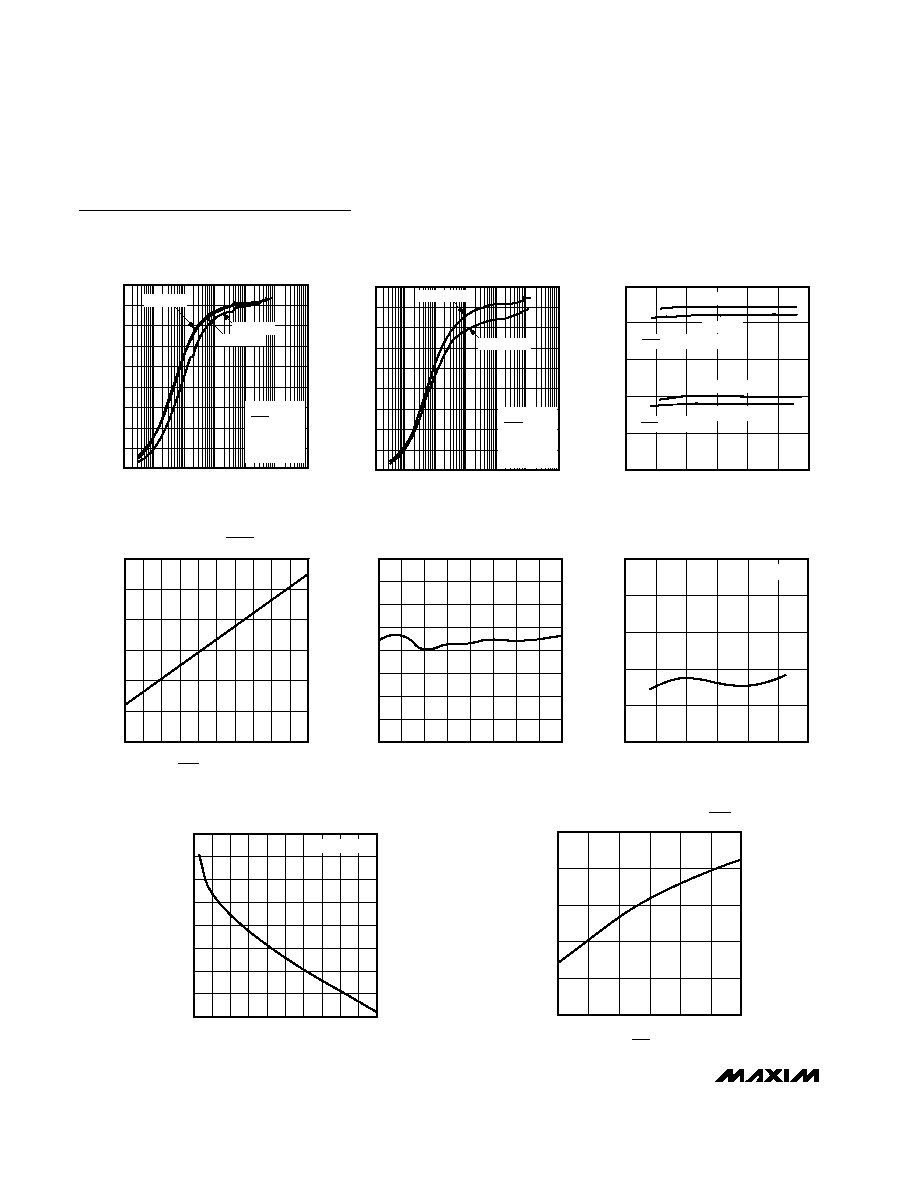
MAX1612/MAX1613
Bridge-Battery Backup Controllers
for Notebooks
4
_______________________________________________________________________________________
Typical Operating Characteristics (continued)
(Circuit of Figure 3, T
A
= +25∞C, unless otherwise noted.)
90
80
70
0
1
µ
10
µ
1m
10m
100m
100
µ
1
EFFICIENCY vs. OUTPUT CURRENT
(BBATT = 2.4V)
MAX612-04
OUTPUT CURRENT (A)
EFFICIENCY (%)
30
20
10
60
50
40
V
OUT
= 7V
V
OUT
= 6V
V
OUT
= 5V
BBATT = 2.4V
R
BBON
= 240k
NOTE: DC-DC
CONVERTER
SUPPLIES V
LRI
90
80
70
0
1
µ
10
µ
1m
10m
100m
100
µ
1
EFFICIENCY vs. OUTPUT CURRENT
(BBATT = 6V)
MAX612-05
OUTPUT CURRENT (A)
EFFICIENCY (%)
30
20
10
60
50
40
BBATT = 3.6V
BBATT = 2.4V
V
OUT
= 6V
R
BBON
= 240k
NOTE: DC-DC
CONVERTER
SUPPLIES V
LRI
0
20
10
40
30
50
0
10
15
5
20
25
30
QUIESCENT CURRENT
vs. LRI VOLTAGE
MAX612-06
V
LRI
(V)
QUIESCENT CURRENT (
µ
A)
MAX1612
MAX1612
MAX1613
MAX1613
R
BBON
= 100k
TO GND
V
BBON
= V
LRO
0
600
400
200
800
1000
1200
5
13
11
7
9
15 17 19 21 23 25
PEAK CURRENT vs. BBON CURRENT
MAX612-07
BBON CURRENT (
µ
A)
PEAK CURRENT (mA)
3.20
3.24
3.22
3.26
3.32
3.30
3.34
3.28
3.36
0
4
6
8
10
2
12 14 16 18 20
MAX1613
LRO VOLTAGE vs. LOAD CURRENT
MAX612-10
LOAD CURRENT (mA)
V
LRO
(V)
V
LRI
= 20V
-2.0
-1.0
-1.5
0
-0.5
0.5
1.0
1.5
2.0
2.0
3.0
3.5
2.5
4.0
4.5
5.0
5.5
6.0
BBATT LEAKAGE CURRENT
vs. BBATT INPUT VOLTAGE
MAX612-08
BBATT INPUT VOLTAGE (V)
BBATT LEAKAGE CURRENT (
µ
A)
3.25
3.27
3.31
3.29
3.33
3.35
0
10
5
15
20
25
30
MAX1613
LRO VOLTAGE vs. LRI VOLTAGE
MAX612-09
V
LRI
(V)
V
LRO
(V)
I
LOAD
= 5mA
100
150
250
200
300
350
120
200
160
240
280
320
360
SWITCHING FREQUENCY vs. R
BBON
MAX612-11
R
BBON
(k
)
SWITCHING FREQUENCY (kHz)

MAX1612/MAX1613
Bridge-Battery Backup Controllers
for Notebooks
_______________________________________________________________________________________
5
NAME
FUNCTION
1
ISET
Bridge-Battery Charge-Current Input. Connect a current-setting resistor from this input to a voltage
higher than the bridge battery. Maximum current rating is 10mA. Pulling ISET below 0.4V resets the
internal counter.
2
BBATT
Bridge-Battery Connection. Bridge-battery charger output.
PIN
3
LX
Step-Up DC-DC Converter N-Channel MOSFET Drain. The maximum operating range is 12V.
4
LBO
Open-Drain Low-Battery Detector Output. When V
LBI
falls below 1.8V, LBO sinks current. When
V
LBI
rises above 2.0V, LBO becomes high impedance.
8
FULL
Open-Drain Bridge-Battery Full Indicator Output. When the internal timer reaches all 1sec, FULL
goes high impedance.
7
CCMD
Charge Command Input. When low with DCMD high, the internal switch from ISET to BBATT is
closed, charging the bridge battery. CCMD is inhibited if DCMD is low. The internal timer counts up
at a frequency set by the CC capacitor.
6
DCMD
Discharge Command Input. When low with CCMD high, the internal timer counts down at a
frequency set by the CD capacitor. When both DCMD and CCMD are low, discharge takes
precedence.
5
BBON
Bridge-Battery On Input. When high, the DC-DC converter turns off. When pulled low through an
external resistor, the resistor sets the peak inductor current. The inductor current is approximately
42,000 times the current in the external resistor (R
BBON
).
13
CD
Discharge Oscillator Capacitor Input. This capacitor sets the discharging oscillator frequency,
which determines the maximum time to decrement the counter from all 1s to all 0s. Calculate the
capacitor value as follows: CD (in nF) = 4.3
∑
discharge time (in hours).
12
CC
Charge Oscillator Capacitor Input. This capacitor programs the charging oscillator frequency,
which sets the time for the internal counter to reach all 1s. Determine the capacitor value by: CC
(in nF) = 4.3
∑
charge time (in hours).
11
GND
Ground
10
LBI
Low-Battery-Detector Input. When LBI falls below 1.8V, LBO goes low and sinks current. When LBI
goes above 2.0V, LBO goes high impedance. Hysteresis is typically 200mV.
9
FB
Feedback Input of Step-Up DC-DC Converter. Regulates to 2V. Connect feedback resistors to set
output voltage (Figure 2).
Pin Description
14
PGND
Power Ground and Step-Up DC-DC Converter N-Channel MOSFET Source
15
LRO
5V (MAX1612) or 3.3V (MAX1613) Linear-Regulator Output. Bypass to GND with a 1µF capacitor.
Maximum external load current is 10mA.
16
LRI
Linear-Regulator Supply Input