 | –≠–ª–µ–∫—Ç—Ä–æ–Ω–Ω—ã–π –∫–æ–º–ø–æ–Ω–µ–Ω—Ç: MAX1638 | –°–∫–∞—á–∞—Ç—å:  PDF PDF  ZIP ZIP |

_______________General Description
The MAX1638 is an ultra-high-performance, step-down
DC-DC controller for CPU power in high-end computer
systems. Designed for demanding applications in which
output voltage precision and good transient response are
critical for proper operation, it delivers over 35A from 1.3V
to 3.5V with ±1% total accuracy from a +5V ±10% supply.
Excellent dynamic response corrects output transients
caused by the latest dynamically clocked CPUs. This
controller achieves over 90% efficiency by using synchro-
nous rectification. Flying-capacitor bootstrap circuitry
drives inexpensive, external N-channel MOSFETs.
The switching frequency is pin-selectable for 300kHz,
600kHz, or 1MHz. High switching frequencies allow the
use of a small surface-mount inductor and decrease out-
put filter capacitor requirements, reducing board area
and system cost.
The MAX1638 is available in 24-pin SSOP and QSOP
(future package) packages, and offers additional fea-
tures such as a digitally programmable output;
adjustable transient response; and selectable 0.5%, 1%,
or 2% AC load regulation. Fast recovery from load tran-
sients is ensured by a GlitchCatcherTM current-boost cir-
cuit that eliminates delays caused by the buck inductor.
Output overvoltage protection is enforced by a crowbar
circuit that turns on the low-side MOSFET with 100%
duty factor when the output is 200mV above the normal
regulation point. Other features include internal digital
soft-start, a power-good output, and a 3.5V ±1% refer-
ence output.
________________________Applications
Pentium ProTM, Pentium IITM, PowerPCTM, AlphaTM,
and K6TM Systems
Workstations
Desktop Computers
LAN Servers
GTL Bus Termination
____________________________Features
o
Better than ±1% Output Accuracy Over
Line and Load
o
Greater than 90% Efficiency Using N-Channel
MOSFETs
o
Pin-Selected High Switching Frequency (300kHz,
600kHz, or 1MHz)
o
Over 35A Output Current
o
Digitally Programmable Output from 1.3V to 3.5V
o
Current-Mode Control for Fast Transient
Response and Cycle-by-Cycle Current-Limit
Protection
o
Short-Circuit Protection with Foldback Current
Limiting
o
Glitch-Catcher Circuit for Fast Load-Transient
Response
o
Crowbar Overvoltage Protection
o
Power-Good (PWROK) Output
o
Digital Soft-Start
o
High-Current (2A) Drive Outputs
o
Complies with Intel VRM 8.2 Specification
MAX1638
High-Speed Step-Down Controller with
Synchronous Rectification for CPU Power
________________________________________________________________
Maxim Integrated Products
1
19-1313; Rev 0; 11/97
PART
MAX1638EAG
MAX1638EEG*
-40∞C to +85∞C
-40∞C to +85∞C
TEMP. RANGE
PIN-PACKAGE
24 SSOP
24 QSOP
______________Ordering Information
__________Typical Operating Circuit
Pin Configuration appears at end of data sheet.
*
Future product--contact factory for package availability.
Pentium Pro and Pentium II are trademarks of Intel Corp.
PowerPC is a trademark of IBM Corp.
Alpha is a trademark of Digital Equipment Corp.
K6 is a trademark of Advanced Micro Devices.
GlitchCatcher is a trademark of Maxim Integrated Products.
V
CC
AGND
REF
LG
FREQ
CC1
CC2
DL
PWROK
D0
LX
BST
DH
PGND
TO V
DD
CSH
OUTPUT
1.3V TO 4.5V
INPUT
+5V
V
DD
CSL
FB
MAX1638
D1
D2
D3
D4
For free samples & the latest literature: http://www.maxim-ic.com, or phone 1-800-998-8800.
For small orders, phone 408-737-7600 ext. 3468.
EVALUATION KIT
AVAILABLE

MAX1638
High-Speed Step-Down Controller with
Synchronous Rectification for CPU Power
2
_______________________________________________________________________________________
ABSOLUTE MAXIMUM RATINGS
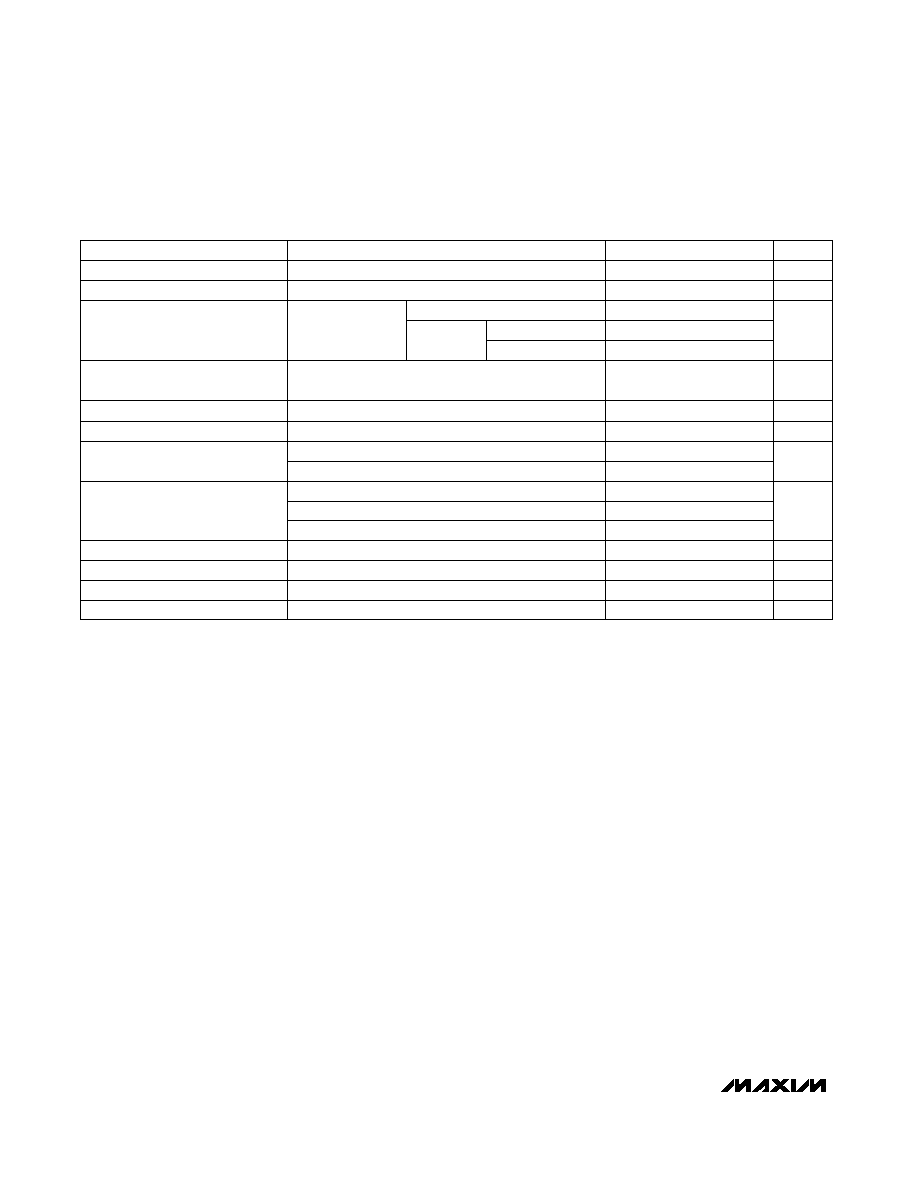
ELECTRICAL CHARACTERISTICS
(V
DD
= V
CC
= D4 = +5V, PGND = AGND = D0≠D3 = 0V, FREQ = REF,
T
A
= 0∞C to +85∞C
, unless otherwise noted.)
Stresses beyond those listed under "Absolute Maximum Ratings" may cause permanent damage to the device. These are stress ratings only, and functional
operation of the device at these or any other conditions beyond those indicated in the operational sections of the specifications is not implied. Exposure to
absolute maximum rating conditions for extended periods may affect device reliability.
V
DD
, V
CC
, PWROK to AGND ......................................-0.3V to 6V
PGND to AGND ..................................................................±0.3V
CSH, CSL to AGND ....................................-0.3V to (V
CC
+ 0.3V)
NDRV, PDRV, DL to PGND.........................-0.3V to (V
DD
+ 0.3V)
REF, CC1, CC2, LG, D0≠D4, FREQ,
FB to AGND .............................................-0.3V to (V
CC
+ 0.3V)
BST to PGND ............................................................-0.3V to 12V
BST to LX ....................................................................-0.3V to 6V
DH to LX.............................................(LX - 0.3V) to (BST + 0.3V)
Continuous Power Dissipation (T
A
= +70∞C)
QSOP (derate 8.70mW/∞C above +70∞C) .....................696mW
QSOP
JC
..................................................................40∞C/W
SSOP (derate 8.00mW/∞C above +70∞C) .....................640mW
SSOP
JC
..................................................................45∞C/W
Operating Temperature Range ...........................-40∞C to +85∞C
Storage Temperature Range .............................-65∞C to +160∞C
Lead Temperature (soldering, 10sec) .............................+300∞C
FREQ = AGND
FREQ = REF
V
CC
= V
DD
FREQ = V
CC
PWROK = 5.5V
Over line and load
(Note 1)
I
SINK
= 2mA, V
CC
= 4.5V
Falling FB, 1% hysteresis with respect to V
REF
Rising FB, 1% hysteresis with respect to V
REF
CSH - CSL =
0mV to 80mV
0µA < I
REF
< 100µA
No load
V
CC
= V
DD
= 5.5V, FB forced 200mV above
regulation point, operating or standby mode
V
CC
rising edge, 1% hysteresis
V
REF
= 0V
Rising edge, 1% hysteresis
CONDITIONS
kHz
255
300
345
Switching Frequency
540
600
660
850
1000
1150
µA
1
PWROK Output Current High
V
0.4
PWROK Output Voltage Low
%
6.5
8
9.5
PWROK Trip Level
-7.5
-6
-4.5
%
2
AC Load Regulation
(Note 2)
1
0.5
mA
0.5
4.0
Reference Short-Circuit Current
V
2.7
3.0
Reference Undervoltage Lockout
V
4.5
5.5
Input Voltage Range
%
±1.5
±1
Output Voltage (FB) Accuracy
mV
10
Reference Load Regulation
V
3.465
3.5
3.535
Reference Voltage
mA
0.1
V
DD
Supply Current
V
4.0
4.2
Input Undervoltage Lockout
UNITS
MIN
TYP
MAX
PARAMETER
CSH - CSL =
0mV to 80mV
%
0.2
DC Load Regulation
(Note 2)
0.1
0.05
T
A
= +25∞C to +85∞C
T
A
= 0∞C to +85∞C
LG = GND
LG = REF
LG = V
CC
LG = GND
LG = REF
LG = V
CC
2.5
FB overdrive = 200mV
5
FB overdrive = 0V
Operating
mode
V
CC
= V
DD
= 5.5V
mA
3.6
10
V
CC
Supply Current
V
REF
= 0V
Shutdown
mode
0.3
DAC code = 11111

ELECTRICAL CHARACTERISTICS (continued)
(V
DD
= V
CC
= D4 = +5V, PGND = AGND = D0≠D3 = 0V, FREQ = REF,
T
A
= 0∞C to +85∞C
, unless otherwise noted.)
MAX1638
_______________________________________________________________________________________
3
DH = DL = 2.5V
V
DD
= 4.5V
BST - LX = 4.5V
GND (low)
100mV overdrive
FREQ = V
CC
With respect to V
REF
,
FB going low
Minimum
D0≠D4 = 0V
D0≠D4, V
CC
= 5.5V
REF (mid)
CSH = CSL = 1.3V, D0≠D3 = 5V, D4 = 0V
D0≠D4, V
CC
= 4.5V
CONDITIONS
-2.75
-2
-1.25
V
CC
(high)
ns
0
30
DH, DL Dead Time
A
2
DH, DL Source/Sink Current
0.7
2
Maximum
DH On-Resistance
0.7
2
%
-3
-1
µA
100
CC2 Source/Sink Current
4
V
CC
V
2.4
3.0
mmho
1
k
10
CC1 Output Resistance
µA
±0.1
3.3
3.7
0.2
%
85
90
Maximum Duty Cycle
LG, FREQ Input Voltage
µA
50
CSH, CSL Input Current
µA
4
LG, FREQ Input Current
µA
2
5
10
D0≠D4 Source Current
V
2.0
Logic Input Voltage High
V
CC
- 0.1
V
0.8
Logic Input Voltage Low
UNITS
MIN
TYP
MAX
PARAMETER
FB Input Current
CC2 Clamp Voltage
CC2 Transconductance
PDRV Trip Level
PDRV, NDRV Response Time
FB overdrive = 5%
ns
75
PDRV, NDRV On-Resistance
V
DD
= 4.5V
2
5
PDRV, NDRV Source/Sink Current
PDRV = NDRV = 2.5V
A
0.5
PDRV, NDRV Minimum On-Time
ns
100
FB = 3.5V
85
100
115
Soft-Start Time
To full current limit
1 / f
OSC
1536
BST Leakage Current
BST = 12V, LX = 7V, REF = GND
µA
50
V
High-Speed Step-Down Controller with
Synchronous Rectification for CPU Power
DL On-Resistance
NDRV Trip Level
With respect to V
REF
,
FB going high
1.25
2
2.75
%
1
3
T
A
= +25∞C
T
A
= 0∞C to +85∞C
T
A
= +25∞C
T
A
= 0∞C to +85∞C
Current-Limit Trip Voltage
FB = 0V (Foldback)
mV
15
38
70
V
MAX1638
High-Speed Step-Down Controller with
Synchronous Rectification for CPU Power
4
_______________________________________________________________________________________
FREQ = REF
FREQ = V
CC
Falling FB, 1% hysteresis with respect to V
REF
Rising FB, 1% hysteresis with respect to V
REF
FREQ = AGND
Over line and load (Note 1)
V
CC
= V
DD
CONDITIONS
510
600
690
800
1000
1200
Switching Frequency
6
8
10
kHz
240
300
360
%
-8
-6
-4
PWROK Trip Level
%
±2.5
Output Voltage (FB) Accuracy
V
4.5
5.5
Input Voltage Range
UNITS
MIN
TYP
MAX
PARAMETER
BST - LX = 4.5V
FREQ = V
CC
V
DD
= 4.5V
0.7
2
%
84
90
0.7
2
Maximum Duty Cycle
DL On-Resistance
DH On-Resistance
FB = 3.5V
Current-Limit Trip Voltage
mV
70
100
130
ELECTRICAL CHARACTERISTICS
(V
DD
= V
CC
= D4 = +5V, PGND = AGND = D0≠D3= 0V, FREQ = REF,
T
A
= -40∞C to +85∞C
, unless otherwise noted.) (Note 3)
Note 1:
FB accuracy is 100% tested at FB = 3.5V (code 10000) with V
CC
= V
DD
= 4.5V to 5.5V and CSH - CSL = 0mV to 80mV. The
other DAC codes are tested with V
CC
= V
DD
= 5V and CSH - CSL = 0.
Note 2:
AC load regulation sets the AC loop gain, to make tradeoffs between output filter capacitor size and transient response,
and has only a slight effect on DC accuracy or DC load-regulation error.
Note 3:
Specifications from 0∞C to -40∞C are guaranteed by design, not production tested.
No load
V
3.448
3.5
3.553
Reference Voltage
V
CC
rising edge, 1% hysteresis
V
3.9
4.3
Input Undervoltage Lockout
0.4
Operating mode
3
V
CC
Supply Current
V
CC
= V
DD
= 5.5V, FB forced 200mV above
regulation point, operating or shutdown mode
mA
0.2
V
CC
= V
DD
= 5.5V,
FB overdrive =
200mV
V
DD
Supply Current
mA
12
Shutdown
mode
V
REF
= 0V
DAC code = 11111
MAX1638
High-Speed Step-Down Controller with
Synchronous Rectification for CPU Power
_______________________________________________________________________________________
5
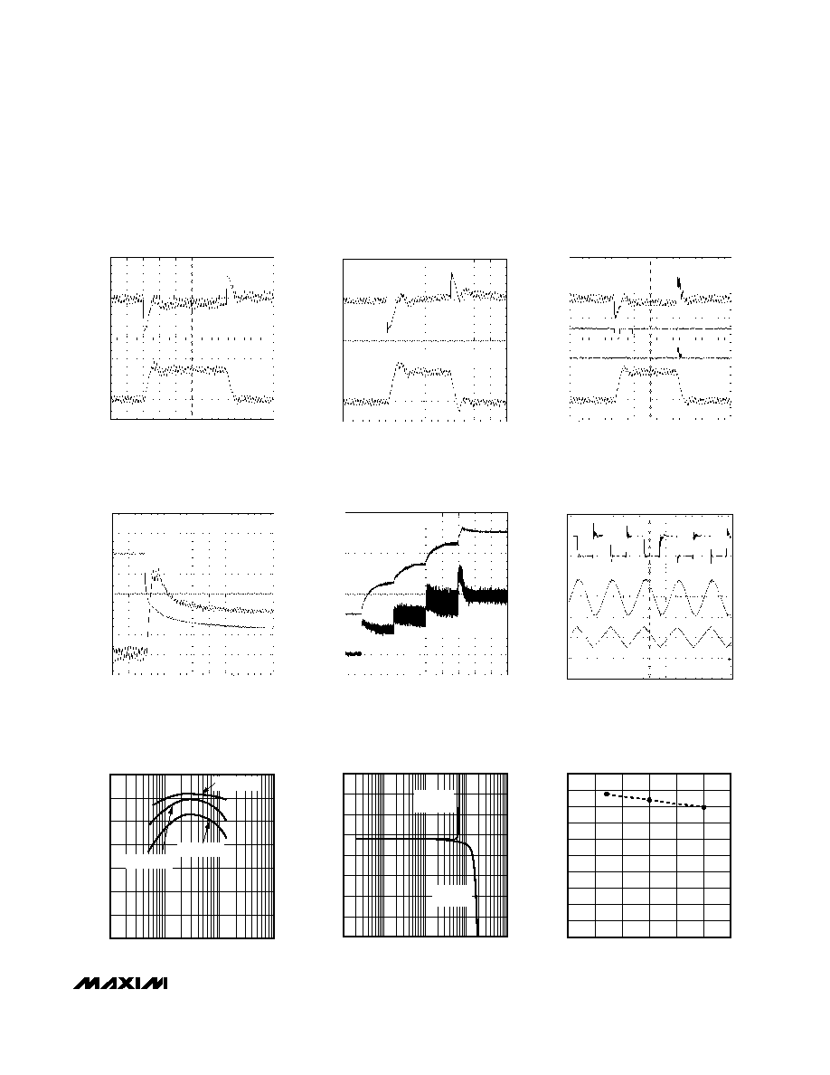
FOLDBACK CURRENT LIMIT
MAX1638-04
V
O
= 2.0V NOMINAL
A: V
OUT
= 0.5V/div
B: INDUCTOR CURRENT, 5A/div
A
B
10
µ
s/div
START-UP WAVEFORMS
MAX1638-05
A: V
OUT
= 0.5V/div
B: INDUCTOR CURRENT, 5A/div
A
B
400
µ
s/div
1
µ
s/div
SWITCHING WAVEFORMS
C
0
MAX1638-06
V
IN
= 5V, V
OUT
= 2.5V, LOAD = 5A
A: LX, 5V/div
C: INDUCTOR CURRENT,
B: V
OUT
, 20mV/div, AC COUPLED
5A/div
B
A
LOAD-TRANSIENT RESPONSE
WITHOUT GLITCHCATCHER (C
OUT
= 880
µ
F)
MAX1638-01
V
IN
= 5V, V
OUT
= 2.0V, LOAD = 14A, 3A/
µ
s
A: V
OUT
, 50mV/div, AC COUPLED
B: INDUCTOR CURRENT, 10A/div
A
B
10
µ
s/div
LOAD-TRANSIENT RESPONSE
WITHOUT GLITCHCATCHER (C
OUT
= 440
µ
F)
MAX1638-02
V
IN
= 5V, V
OUT
= 2.0V, LOAD = 14A, 3A/
µ
s
A: V
OUT
, 100mV/div, AC COUPLED
B: INDUCTOR CURRENT, 10A/div
A
B
10
µ
s/div
LOAD-TRANSIENT RESPONSE
WITH GLITCHCATCHER
MAX1638-03
C
OUT
= 440
µ
F, V
IN
= 5V, V
OUT
= 2.0V, LOAD = 14A, 30A/
µ
s
A: V
OUT
, 100mV/div,
C: NDRV, 5V/div
AC COUPLED
D: INDUCTOR CURRENT,
B: PDRV, 5V/div
10A/div
A
D
B
C
10
µ
s/div
__________________________________________Typical Operating Characteristics
(T
A
= +25∞C, using the MAX1638 evaluation kit, unless otherwise noted.)
100
90
30
0.1
10
100
EFFICIENCY vs. OUTPUT CURRENT
50
40
80
70
60
MAX1638-07
OUTPUT CURRENT (A)
EFFICIENCY (%)
1
V
OUT
= 2.0V
V
OUT
= 1.3V
V
OUT
= 3.5V
5.094
1.094
0.001
0.1
1
0.01
10
REFERENCE VOLTAGE
vs. OUTPUT CURRENT
1.594
2.094
MAX1638-08
OUTPUT CURRENT (mA)
REFERENCE VOLTAGE (V)
2.594
3.594
3.094
4.094
4.594
SOURCING
CURRENT
SINKING
CURRENT
50
55
0
MAXIMUM DUTY CYCLE
vs. SWITCHING FREQUENCY
65
60
70
MAX1638-09
SWITCHING FREQUENCY (kHz)
MAXIMUM DUTY CYCLE (%)
85
95
90
75
80
200
800
1000
1200
100
600
400