 | –≠–ª–µ–∫—Ç—Ä–æ–Ω–Ω—ã–π –∫–æ–º–ø–æ–Ω–µ–Ω—Ç: MAX1639 | –°–∫–∞—á–∞—Ç—å:  PDF PDF  ZIP ZIP |

________________General Description
The MAX1639 is an ultra-high-performance, step-down
DC-DC controller for CPU power in high-end computer
systems. Designed for demanding applications in which
output voltage precision and good transient response are
critical for proper operation, it delivers over 35A from 1.1V
to 4.5V with ±1% total accuracy from a +5V ±10% supply.
Excellent dynamic response corrects output transients
caused by the latest dynamically clocked CPUs. This
controller achieves over 90% efficiency by using synchro-
nous rectification. Flying-capacitor bootstrap circuitry
drives inexpensive, external N-channel MOSFETs.
The switching frequency is pin-selectable for 300kHz,
600kHz, or 1MHz. High switching frequencies allow the
use of a small surface-mount inductor and decrease out-
put filter capacitor requirements, reducing board area
and system cost.
Output overvoltage protection is enforced by a crowbar
circuit that turns on the low-side MOSFET with 100%
duty factor when the output is 200mV above the normal
regulation point. Other features include internal digital
soft-start, a power-good output, and a 3.5V ±1% refer-
ence output. The MAX1639 is available in a 16-pin
narrow SOIC package.
________________________Applications
Local DC-DC Converters for CPUs
Workstations
Desktop Computers
LAN Servers
GTL Bus Termination
____________________________Features
o
Better than ±1% Output Accuracy Over
Line and Load
o
Greater than 90% Efficiency Using N-Channel
MOSFETs
o
Pin-Selected High Switching Frequency:
300kHz, 600kHz, or 1MHz
o
Over 35A Output Current
o
Resistor-Divider Adjustable Output from
1.1V to 4.5V
o
Current-Mode Control for Fast Transient
Response and Cycle-by-Cycle Current-Limit
Protection
o
Short-Circuit Protection with Foldback Current
Limiting
o
Crowbar Overvoltage Protection
o
Power-Good (PWROK) Output
o
Digital Soft-Start
o
High-Current (2A) Drive Outputs
MAX1639
High-Speed Step-Down Controller with
Synchronous Rectification for CPU Power
________________________________________________________________
Maxim Integrated Products
1
19-1337; Rev 0; 2/98
PART
MAX1639ESE
-40∞C to +85∞C
TEMP. RANGE
PIN-PACKAGE
16 Narrow SO
_______________Ordering Information
__________ Typical Operating Circuit
Pin Configuration appears at end of data sheet.
V
CC
AGND
REF
FREQ
CC1
CC2
DL
PWROK
LX
BST
DH
PGND
TO V
DD
CSH
OUTPUT
1.1V TO 4.5V
INPUT
+5V
V
DD
CSL
FB
MAX1639
For free samples & the latest literature: http://www.maxim-ic.com, or phone 1-800-998-8800.
For small orders, phone 408-737-7600 ext. 3468.
EVALUATION KIT
AVAILABLE

FREQ Input Voltage
MAX1639
High-Speed Step-Down Controller with
Synchronous Rectification for CPU Power
2
_______________________________________________________________________________________
ABSOLUTE MAXIMUM RATINGS
ELECTRICAL CHARACTERISTICS
(V
DD
= V
CC
= +5V, PGND = AGND = 0V, FREQ = REF,
T
A
= 0∞C to +85∞C
, unless otherwise noted.)
Stresses beyond those listed under "Absolute Maximum Ratings" may cause permanent damage to the device. These are stress ratings only, and functional
operation of the device at these or any other conditions beyond those indicated in the operational sections of the specifications is not implied. Exposure to
absolute maximum rating conditions for extended periods may affect device reliability.
V
DD
, V
CC
, PWROK to AGND ....................................-0.3V to +6V
PGND to AGND ..................................................................±0.3V
CSH, CSL to AGND ....................................-0.3V to (V
CC
+ 0.3V)
DL to PGND................................................-0.3V to (V
DD
+ 0.3V)
REF, CC1, CC2, FREQ, FB to AGND .........-0.3V to (V
CC
+ 0.3V)
BST to PGND..........................................................-0.3V to +12V
BST to LX..................................................................-0.3V to +6V
DH to LX.............................................(LX - 0.3V) to (BST + 0.3V)
Continuous Power Dissipation (T
A
= +70∞C)
16-Pin Narrow SO (derate 8.70mW/∞C above +70∞C) ....696mW
SO
JC
...........................................................................65∞C/W
Operating Temperature Range
MAX1639ESE....................................................-40∞C to +85∞C
Storage Temperature Range .............................-65∞C to +160∞C
Lead Temperature (soldering, 10sec) .............................+300∞C
FREQ = AGND
FREQ = REF
V
CC
= V
DD
FREQ = V
CC
PWROK = 5.5V
Includes line and load
regulation errors
I
SINK
= 2mA, V
CC
= 4.5V
Falling FB, 1% hysteresis with respect to V
REF
Rising FB, 1% hysteresis with respect to V
REF
0µA < I
REF
< 100µA
No load
V
CC
= V
DD
= 5.5V, FB forced 60mV above
regulation point, operating or standby mode
V
CC
rising edge, 1% hysteresis
V
REF
= 0V
Rising edge, 1% hysteresis
CONDITIONS
kHz
255
300
345
Switching Frequency
540
600
660
850
1000
1150
µA
1
PWROK Output Current High
V
0.4
PWROK Output Voltage Low
%
6.5
8
9.5
PWROK Trip Level
-7.5
-6
-4.5
mA
0.5
4.0
Reference Short-Circuit Current
V
2.7
3.0
Reference Undervoltage Lockout
V
4.5
5.5
Input Voltage Range
V
1.083
1.117
1.089
1.111
FB Voltage
mV
10
Reference Load Regulation
V
3.465
3.5
3.535
Reference Voltage
mA
0.1
V
DD
Supply Current (I
DD
)
V
4.0
4.2
Input Undervoltage Lockout
UNITS
MIN
TYP
MAX
PARAMETER
T
A
= +25∞C to +85∞C
T
A
= 0∞C to +85∞C
2.5
5
CSH - CSL = 0mV to 80mV
%
1
AC Load Regulation
CSH - CSL = 0mV to 80mV
%
0.1
DC Load Regulation
FB overdrive = 60mV
FB overdrive = 0V
Operating
mode
mA
3.6
10
V
CC
= V
DD
= 5.5V
V
REF
= 0V
Shutdown
mode
V
CC
Supply Current (I
CC
)
V
CC
(high)
GND (low)
FREQ = V
CC
%
V
CC
- 0.1
Maximum Duty Cycle
0.2
85
90
FREQ Input Voltage
V
REF (mid)
3.3
3.7

ELECTRICAL CHARACTERISTICS (continued)
(V
DD
= V
CC
= +5V, PGND = AGND = 0V, FREQ = REF,
T
A
= 0∞C to +85∞C
, unless otherwise noted.)
MAX1639
_______________________________________________________________________________________
3
High-Speed Step-Down Controller with
Synchronous Rectification for CPU Power
15
38
70
mV
FB = 0V (foldback)
Current-Limit Trip Voltage
DL On-Resistance
50
µA
BST = 12V, LX = 7V, REF = GND
BST Leakage Current
1536
1 / f
OSC
To full current limit
Soft-Start Time
85
100
115
FB = 1.1V
FB Input Current
CC2 Clamp Voltage
PARAMETER
MIN
TYP
MAX
UNITS
FREQ Input Current
4
µA
±0.1
µA
2.4
3.0
V
4
V
CC
CC2 Source/Sink Current
100
µA
0.7
2
DH On-Resistance
Maximum
0.7
2
DH, DL Source/Sink Current
2
A
DH, DL Dead Time
0
30
ns
CONDITIONS
Minimum
30mV overdrive
BST - LX = 4.5V
V
DD
= 4.5V
DH = DL = 2.5V
ELECTRICAL CHARACTERISTICS
(V
DD
= V
CC
= +5V, PGND = AGND = 0V, FREQ = REF,
T
A
= -40∞C to +85∞C
, unless otherwise noted.) (Note 1)
Note 1:
Specifications from 0∞C to -40∞C are guaranteed by design, not production tested.
FREQ = REF
FREQ = V
CC
BST - LX = 4.5V
FREQ = V
CC
Falling FB, 1% hysteresis with respect to V
REF
Rising FB, 1% hysteresis with respect to V
REF
FREQ = AGND
V
DD
= 4.5V
2
%
84
DL On-Resistance
V
CC
rising edge, 1% hysteresis
V
CC
= V
DD
2
CONDITIONS
510
690
Maximum Duty Cycle
800
1200
DH On-Resistance
Switching Frequency
FB = 1.1V
Current-Limit Trip Voltage
mV
70
130
6
10
kHz
240
360
%
-8
-4
PWROK Trip Level
V
3.9
4.3
Input Undervoltage Range
V
4.5
5.5
Input Voltage Range
UNITS
MIN
TYP
MAX
PARAMETER
CC2 Transconductance
CC1 Output Resistance
10
k
1
mmho
CSH, CSL Input Current
50
µA
CSH = CSL = 1.1V
V
CC
= V
DD
=
5.5V
mA
12
V
DD
Supply Current
3
Includes line and load regulation errors
No load
V
1.072
1.128
FB Voltage
V
3.448
3.553
Reference Voltage
V
CC
= V
DD
= 5.5V, FB forced 60mV above
regulation point, operating or shutdown mode
mA
0.2
V
DD
Supply Current
Operating mode
FB overdrive = 60mV
VREF = 0V
Shutdown mode
MAX1639
High-Speed Step-Down Controller with
Synchronous Rectification for CPU Power
4
_______________________________________________________________________________________
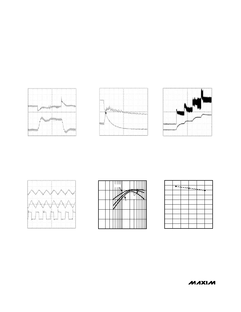
FOLDBACK CURRENT LIMIT
(V
OUT
= 2.5V, NOMINAL)
MAX1639-02
A: V
OUT
= 0.5V/div
B: INDUCTOR CURRENT, 5A/div
A
B
10
µ
s/div
START-UP WAVEFORMS
MAX1639-03
A: INDUCTOR CURRENT, 2A/div
B: V
OUT
= 1V/div
A
B
400
µ
s/div
1
µ
s/div
SWITCHING WAVEFORMS
C
0
MAX1639-04
V
IN
= 5V, V
OUT
= 2.5V, LOAD = 0A
A: V
OUT
, 20mV/div
B: INDUCTOR CURRENT, 2A/div
C: LX, 5V/div
B
A
LOAD-TRANSIENT RESPONSE
(V
OUT
= 2.5V)
MAX1639-01
V
IN
= 5V, V
OUT
= 2.5V, LOAD = 8A
A: V
OUT
, 100mV/div, AC COUPLED
B: INDUCTOR CURRENT, 5A/div
A
B
10
µ
s/div
__________________________________________Typical Operating Characteristics
(T
A
= +25∞C, using the MAX1639 evaluation kit, unless otherwise noted.)
100
50
0.1
10
EFFICIENCY vs. OUTPUT CURRENT
60
90
80
70
MAX1639-05
OUTPUT CURRENT (A)
EFFICIENCY (%)
1
3.5V
1.8V
2.5V
50
55
0
MAXIMUM DUTY CYCLE vs.
SWITCHING FREQUENCY
65
60
70
MAX1639-06
SWITCHING FREQUENCY (kHz)
MAXIMUM DUTY CYCLE (%)
85
95
90
75
80
200
800
1000
1200
100
600
400
MAX1639
High-Speed Step-Down Controller with
Synchronous Rectification for CPU Power
_______________________________________________________________________________________
5
______________________________________________________________Pin Description
7
Analog Ground
AGND
6
Reference Output, 3.5V. Bypass REF to AGND with 0.1µF (min). Sources up to 100µA for external
loads. Force REF below 2V to turn off the controller.
REF
5
Analog Supply Input, 5V. Use an RC filter network, as shown in Figure 1.
V
CC
4
Current-Sense Amplifier's Noninverting Input
CSH
3
Current-Sense Amplifier's Inverting Input. Place the current-sense resistor very close to the controller IC,
and use a Kelvin connection.
CSL
2
Open-Drain Logic Output. PWROK is high when the voltage on FB is within +8% and -6% of its set-
point.
PWROK
8
Voltage-Feedback Input. The voltage at this input is regulated to 1.100V.
FB
9
Fast-Loop Compensation Capacitor Input. Connect a ceramic capacitor and resistor in series from
CC1 to AGND. See the section
Compensating the Feedback Loop.
CC1
FUNCTION
NAME
1
Boost-Capacitor Bypass for High-Side MOSFET Gate Drive. Connect a 0.1µF capacitor and low-leak-
age Schottky diode as a bootstrapped charge-pump circuit to derive a 5V gate drive from V
DD
for DH.
BST
10
Slow-Loop Compensation Capacitor Input. Connect a ceramic capacitor from CC2 to AGND. See the
section
Compensating the Feedback Loop.
CC2
11
Frequency-Select Input. FREQ = V
CC
: 1MHz
FREQ = REF: 600kHz
FREQ = AGND: 300kHz
FREQ
12
Power Input for MOSFET Drivers, 5V. Bypass V
DD
to PGND within 0.2 in. (5mm) of the V
DD
pin using a
0.1µF capacitor and 4.7µF capacitor connected in parallel.
V
DD
13
Low-Side Synchronous Rectifier Gate-Drive Output. DL swings between PGND and V
DD
. See the
section
BST High-Side Gate-Driver Supply and MOSFET Drivers.
DL
14
PGND
Power Ground
15
LX
Switching Node. Connect LX to the high-side MOSFET source and inductor.
16
DH
High-Side Main MOSFET Switch Gate-Drive Output. DH is a floating driver output that swings from LX
to BST, riding on the LX switching-node voltage. See the section
BST High-Side Gate-Driver Supply
and MOSFET Drivers.
PIN