 | –≠–Ľ–Ķ–ļ—ā—Ä–ĺ–Ĺ–Ĺ—č–Ļ –ļ–ĺ–ľ–Ņ–ĺ–Ĺ–Ķ–Ĺ—ā: MAX1660 | –°–ļ–į—á–į—ā—Ć:  PDF PDF  ZIP ZIP |
General Description
The MAX1660 digitally controlled fuel-gauge interface
executes two essential functions for rechargeable bat-
tery-pack management: fuel gauging and pack overcur-
rent protection. It accurately monitors a battery pack's
charge and discharge current flow, and records each
using two independent, on-board Coulomb counters.
Each counter's contents are externally accessible via a
System Management Bus (SMBusTM)-compatible 2-wire
serial interface. An optional third wire interrupts the
microcontroller (ĶC) when the charge or discharge
counters reach a preset value, or when an overcurrent
condition (charge or discharge) occurs. In the event of
an overcurrent or short-circuit condition, the MAX1660
disconnects the load and alerts its host. The MAX1660's
flexibility allows accurate fuel gauging for any battery
chemistry, using any desired control algorithm.
The MAX1660 operates with battery voltages from +4V
to +28V and provides two micropower shutdown
modes, increasing battery lifetime. To minimize total
parts count, the device integrates a precision 2.00V
system-reference output, a 3.3V linear-regulator output
that can supply up to 5mA to power external circuitry,
and a power-on reset output for the system ĶC. The
MAX1660 is available in a 16-pin QSOP package.
________________________Applications
Smart-Battery Packs
Battery-Pack Fuel Gauging
Battery-Pack Overcurrent
Digital Current-Sense
Protection
Instrumentation
Industrial-Control System
Analog-to-Digital
Interfaces
Conversion
____________________________Features
o
1% Accuracy over a 600ĶA to 4A Current Range
(R
SENSE
= 30m
)
o
5ĶV Input Offset Voltage (28ĶV max)
o
SMBus 2-Wire (plus optional interrupt)
Serial Interface
o
2.00V Precision System Reference Output
o
3.3V Linear-Regulator Output Powers External
Circuitry
o
Two Micropower Shutdown Modes
o
Independent 32-Bit Charge and Discharge
Coulomb Counters
o
Battery-Overcharge/Overdischarge Protection
o
Battery Short-Circuit/Overcurrent Protection
o
On-Board Power MOSFET Drivers
o
80ĶA Quiescent Current
o
<1ĶA Shutdown Current
o
Small 16-Pin QSOP Package
(same board area as 8-pin SO)
MAX1660
*
Digitally Controlled
Fuel-Gauge Interface
________________________________________________________________
Maxim Integrated Products
1
19-1308; Rev 1; 10/98
EVALUATION KIT MANUAL
FOLLOWS DATA SHEET
SMBus is a trademark of Intel Corp.
*
Patent pending
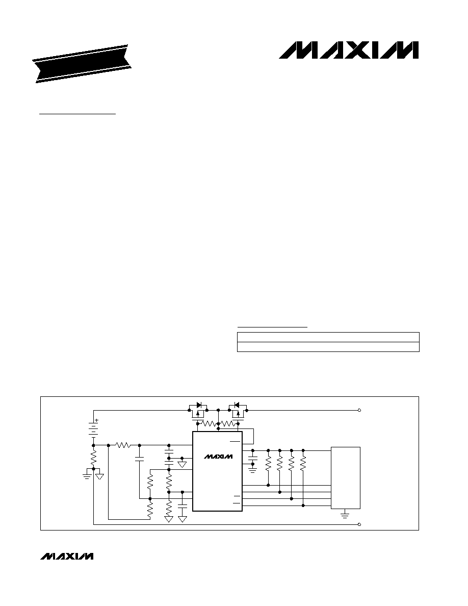
MAX1660
BATT
CS
AGND
REF
OCI
ODI
GND
SCL
SDA
SHDN
OCO
VL
V
CC
GND
PACK-
PACK+
Ķ
C
RST
INT
ODO
R
CS
___________________________________________________Typical Operating Circuit
For free samples & the latest literature: http://www.maxim-ic.com, or phone 1-800-998-8800.
For small orders, phone 1-800-835-8769.
PART
MAX1660EEE
-40įC to +85įC
TEMP. RANGE
PIN-PACKAGE
16 QSOP
Ordering Information
Pin Configuration appears at end of data sheet.

*
Patent pending
MAX1660
*
Digitally Controlled
Fuel-Gauge Interface
2
_______________________________________________________________________________________
ABSOLUTE MAXIMUM RATINGS
ELECTRICAL CHARACTERISTICS
(V
SHDN
= V
BATT
= 12V, V
SCL
= V
SDA
= 3.6V, C
REF
= 10nF, C
VL
= 0.1ĶF,
T
A
= 0įC to +85įC
, unless otherwise noted. Typical values
are at T
A
= +25įC.)
Stresses beyond those listed under "Absolute Maximum Ratings" may cause permanent damage to the device. These are stress ratings only, and functional
operation of the device at these or any other conditions beyond those indicated in the operational sections of the specifications is not implied. Exposure to
absolute maximum rating conditions for extended periods may affect device reliability.
BATT, ODO, OCO, SHDN to GND .........................-0.3V to +30V
SCL, SDA, INT, RST to GND ....................................-0.3V to +6V
REF, ODI, OCI to GND..................................-0.3V to (VL + 0.3V)
VL to GND ................................................................-0.3V to +6V
CS to GND...................................................................-2V to +6V
AGND to GND .............................................................-1V to +1V
Continuous Power Dissipation (T
A
= +70įC)
16-Pin QSOP (derate 8.3mW/įC above +70įC).............667mW
Operating Temperature Range ...........................-40įC to +85įC
Storage Temperature Range .............................-65įC to +165įC
Lead Temperature (soldering, 10sec) .............................+300įC
V
OCO
= 0.4V
V
ODO
= 28V
V
SHDN
= 3.3V, SOFTSHDN = 0, I
VL
= 0
V
ODO
= 0.4V
(Note 1)
V
CS
= 120mV
V
CS
= 0
0
I
REF
200ĶA
I
REF
= 0
V
SHDN
= 3.3V, SOFTSHDN = 1, I
VL
= 0
V
SHDN
0.4V
SOFTSHDN = 0, 0
I
VL
5mA
V
CS
= -120mV
SOFTSHDN = 1, 0
I
VL
5mA
V
CS
= 0
CONDITIONS
mA
1
2.5
OCO Sink Current
ĶA
0.01
1
ODO Off-Leakage Current
mA
1
2.5
ODO Sink Current
Ķs
1
Propagation Delay
ĶA
-1
0.01
1
OCI, ODI Input Offset Current
mV
-7
0
7
OCI, ODI Input Offset Voltage
49,500
50,000
50,500
counts/
sec
0
2
12
Charge Coulomb-Counter
Accumulation Rate
49,500
50,000
50,500
counts/
sec
0
2
12
Discharge Coulomb-Counter
Accumulation Rate
ĶA
80
135
I
BATT
BATT Supply Current
V
4
28
V
BATT
BATT Input Voltage Range
k
100
CS to AGND Input Resistance
ĶV/ĶA
10
50
REF Load Regulation
V
1.96
2.00
2.04
V
REF
REF Output Voltage
15
30
0.02
1
V
3.1
3.25
3.4
V
VL
VL Output Voltage
3.1
3.25
3.6
UNITS
MIN
TYP
MAX
SYMBOL
PARAMETER
V
INT
= 0.4V
V
SDA
= 0.6V
SHDN
SCL, SDA
SHDN, SCL, SDA
V
OCO
= 28V
mA
2
V
OL
INT Output Low Sink Current
mA
6
V
OL
SDA Output Low Sink Current
0.6
V
0.8
V
IL
Input Low Voltage
V
2.2
V
IH
Input High Voltage
ĶA
0.01
1
OCO Off-Leakage Current
SUPPLY AND REFERENCES
FUEL GAUGE
OVERCURRENT COMPARATOR
INTERFACE-LOGIC LEVELS
MAX1660
*
Digitally Controlled
Fuel-Gauge Interface
_______________________________________________________________________________________
3
ELECTRICAL CHARACTERISTICS (continued)
(V
SHDN
= V
BATT
= 12V, V
SCL
= V
SDA
= 3.6V, C
REF
= 10nF, C
VL
= 0.1ĶF,
T
A
= 0įC to +85įC
, unless otherwise noted. Typical values
are at T
A
= +25įC.)
V
TH1
, VL rising
V
VL
= 3V, I
SINK
= 1.2mA
CONDITIONS
V
VL
= 1V, I
SINK
= 50ĶA
V
TH2
, VL falling
2.75
2.90
3.05
V
1.0
1.7
2.2
0.3
V
0.3
V
RST
RST Output Voltage
V
TH1
,
V
TH2
RST Threshold Voltage
UNITS
MIN
TYP
MAX
SYMBOL
PARAMETER
SHDN forced to 28V
SHDN forced to 3.6V
Output forced to 5V
ms
25
RST Active Timeout Period
20
100
ĶA
0.7
3.0
I
SHDN
SHDN Input Bias Current
ĶA
0.01
1
SCL, SDA, INT, RST Leakage
Current
V
ODO
= 0.4V
V
ODO
= 28V
V
SHDN
= 3.3V, SOFTSHDN = 0, I
VL
= 0
V
ODO
= 0.4V
(Note 1)
V
CS
= 120mV
V
CS
= 0
0
I
REF
200ĶA
I
REF
= 0
V
SHDN
= 3.3V, SOFTSHDN = 1, I
VL
= 0
V
SHDN
0.4V
SOFTSHDN = 0, 0
I
VL
5mA
V
CS
= -120mV
SOFTSHDN = 1, 0
I
VL
5mA
V
CS
= 0
CONDITIONS
mA
1
OCO Sink Current
ĶA
1
ODO Off-Leakage Current
mA
1
ODO Sink Current
ĶA
-1
1
OCI, ODI Input Offset Current
mV
-10
10
OCI, ODI Input Offset Voltage
49,250
50,750
counts/
sec
0
12
Charge Coulomb-Counter
Accumulation Rate
counts/
sec
0
12
Discharge Coulomb-Counter
Accumulation Rate
ĶA
135
I
BATT
BATT Supply Current
V
4
28
V
BATT
BATT Input Voltage Range
ĶV/ĶA
50
REF Load Regulation
V
1.96
2.04
V
REF
REF Output Voltage
30
1
V
3.1
3.4
V
VL
VL Output Voltage
3.1
3.6
UNITS
MIN
TYP
MAX
SYMBOL
PARAMETER
V
ODO
= 28V
ĶA
1
OCO Off-Leakage Current
ELECTRICAL CHARACTERISTICS
(V
SHDN
= V
BATT
= 12V, V
SCL
= V
SDA
= 3.6V, C
REF
= 10nF, C
VL
= 0.1ĶF,
T
A
= -40įC to +85įC
, unless otherwise noted.) (Note 2)
SUPPLY AND REFERENCES
FUEL GAUGE
OVERCURRENT COMPARATOR
*
Patent pending

*
Patent pending
MAX1660
*
Digitally Controlled
Fuel-Gauge Interface
4
_______________________________________________________________________________________
V
TH1
, VL rising
V
VL
= 3V, I
SINK
= 1.2mA
CONDITIONS
V
VL
= 1V, I
SINK
= 50ĶA
V
TH2
, VL falling
2.75
3.05
V
1.0
2.2
0.3
V
0.3
V
RST
RST Output Voltage
V
TH1
,
V
TH2
RST Threshold Voltage
UNITS
MIN
TYP
MAX
SYMBOL
PARAMETER
SHDN forced to 28V
SHDN forced to 3.6V
Output forced to 5V
V
INT
= 0.4V
V
SDA
= 0.6V
SHDN
SCL, SDA
SHDN, SCL, SDA
120
ĶA
3.0
I
SHDN
SHDN Input Bias Current
ĶA
1
SCL, SDA, INT, RST Leakage
Current
mA
2
V
OL
INT, RST Output Low Sink Current
mA
6
V
OL
SDA Output Low Sink Current
0.6
V
0.8
V
IL
Input Low Voltage
V
2.2
V
IH
Input High Voltage
ELECTRICAL CHARACTERISTICS (continued)
(V
SHDN
= V
BATT
= 12V, V
SCL
= V
SDA
= 3.6V, C
REF
= 10nF, C
VL
= 0.1ĶF,
T
A
= -40įC to +85įC
, unless otherwise noted.) (Note 2)
TIMING CHARACTERISTICS
(
T
A
= 0įC to +85įC
, unless otherwise noted.)
CONDITIONS
Ķs
4.7
t
SU:STA
Start-Condition Setup Time
Ķs
4.7
t
LOW
Ķs
4
t
HIGH
SCL Serial-Clock High Period
SCL Serial-Clock Low Period
Ķs
4
t
HD:STA
Start-Condition Hold Time
ns
800
t
SU:DAT
SDA Valid to SCL Rising-Edge Setup
Time, Slave Clocking in Data
ns
0
t
HD:DAT
SCL Falling Edge to SDA Transition
Ķs
1
t
DV
SCL Falling Edge to SDA Valid, Master
Clocking in Data
UNITS
MIN
TYP
MAX
SYMBOL
PARAMETER
INTERFACE-LOGIC LEVELS
MAX1660
*
Digitally Controlled
Fuel-Gauge Interface
_______________________________________________________________________________________
5
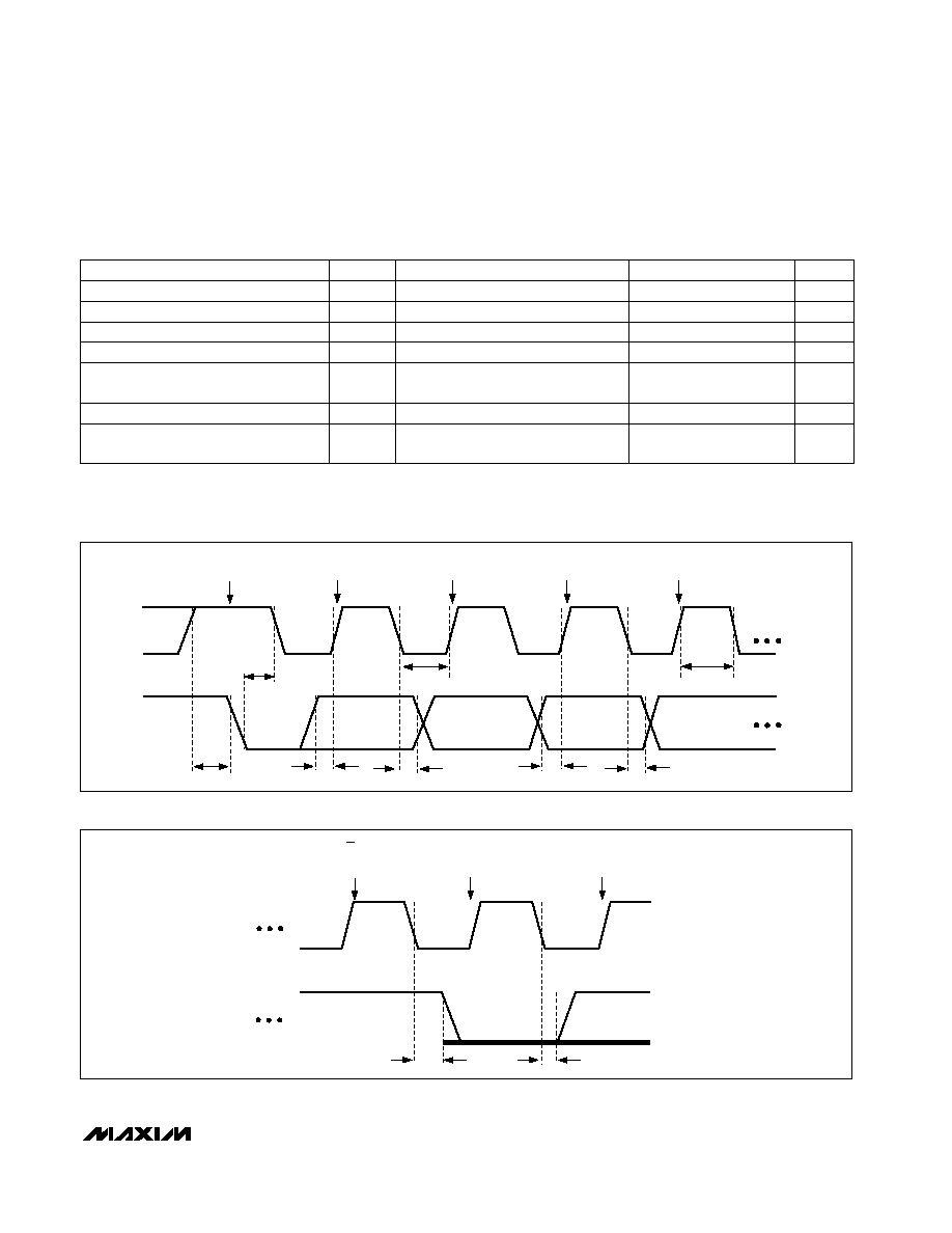
SCL
START
CONDITION
t
HIGH
SDA
t
LOW
t
HD:STA
t
SU:STA
t
SU:DAT
t
HD:DAT
t
SU:DAT
t
HD:DAT
MOST SIGNIFICANT ADDRESS BIT
(A6) CLOCKED INTO SLAVE
A5 CLOCKED
INTO SLAVE
A4 CLOCKED
INTO SLAVE
A3 CLOCKED
INTO SLAVE
Note 1:
OCI and ODI are MOSFET inputs. Minimum and maximum limits are for production screening only. Actual performance is
indicated in typical value.
Note 2:
Specifications to -40įC are guaranteed by design, not production tested.
CONDITIONS
Ķs
1
t
DV
SCL Falling Edge to SDA Valid, Master
Clocking in Data
ns
0
t
HD:DAT
SCL Falling Edge to SDA Transition
ns
800
t
SU:DAT
SDA Valid to SCL Rising-Edge Setup
Time, Slave Clocking in Data
Ķs
4
t
HD:STA
Start-Condition Hold Time
Ķs
4.7
t
SU:STA
Start-Condition Setup Time
Ķs
4.7
t
LOW
SCL Serial-Clock Low Period
Ķs
4
t
HIGH
SCL Serial-Clock High Period
UNITS
MIN
TYP
MAX
SYMBOL
PARAMETER
TIMING CHARACTERISTICS
(
T
A
= -40įC to +85įC
, unless otherwise noted.) (Note 2)
Figure 1. SMBus Serial-Interface Timing--Address
SCL
RW BIT
CLOCKED
INTO SLAVE
SDA
t
DV
t
DV
ACKNOWLEDGE
BIT CLOCKED
INTO MASTER
SLAVE PULLING
SDA LOW
MOST SIGNIFICANT BIT
OF DATA CLOCKED
INTO MASTER
Figure 2. SMBus Serial-Interface Timing--Acknowledge
*
Patent pending