 | –≠–ª–µ–∫—Ç—Ä–æ–Ω–Ω—ã–π –∫–æ–º–ø–æ–Ω–µ–Ω—Ç: MAX1663 | –°–∫–∞—á–∞—Ç—å:  PDF PDF  ZIP ZIP |

x
For free samples & the latest literature: http://www.maxim-ic.com, or phone 1-800-998-8800.
For small orders, phone 408-737-7600 ext. 3468.
________________General Description
The MAX1661/MAX1662/MAX1663 serial-to-parallel/
parallel-to-serial converters are intended to control external
power MOSFETs in power-plane switching applications.
These small, low-cost devices can be used on a system
motherboard to control point-of-load switching from a 2-
wire SMBusTM serial interface. Each device has three high-
voltage open-drain outputs that double as TTL-level logic
inputs, giving them bidirectional capabilities. The I/O pins
can withstand +28V, so they can control battery voltage-
distribution switches in notebook computers.
The MAX1661 is intended for driving N-channel MOSFETs
and its outputs are low upon power-up. The MAX1662/
MAX1663 are intended for P-channel MOSFETs, and their
outputs are high-impedance upon power-up. This ensures
that the MOSFETs are off at power-up, so the system can
enforce power-plane sequencing.
The SMBSUS control input selects control data between
two separate data registers. This feature allows the system
to select between two different power-plane configurations
asynchronously, eliminating latencies introduced by the
serial bus. Other features include thermal-overload and
overcurrent protection, ultra-low supply current, and both
hardware and software interrupt capabilities. These
devices are available in the space-saving 10-pin µMAX
package.
________________________Applications
Power-Plane Switching
Point-of-Load Power-Bus Switching
Notebook and Subnotebook Computers
Desktop Computers
Smart Batteries
____________________________Features
o
Performs Serial-to-Parallel and Parallel-to-Serial
Conversions
o
Three General-Purpose Digital Input/Output Pins
(withstand +28V)
o
SMBus 2-Wire Serial Interface
o
Supports
SMBSUS
Asynchronous Suspend Mode
o
3µA Supply Current
o
+2.7V to +5.5V Supply Range
o
Space-Saving, Low-Cost 10-Pin µMAX Package
MAX1661/MAX1662/MAX1663
________________________________________________________________
Maxim Integrated Products
1
1
2
3
4
5
10
9
8
7
6
ALERT
SMBCLK
SMBDATA
SMBSUS
I/O3
I/O2
I/O1
V
CC
MAX1661
MAX1662
MAX1663
µ
MAX
TOP VIEW
ADD
GND
__________________Pin Configuration
19-1306; Rev 0; 10/97
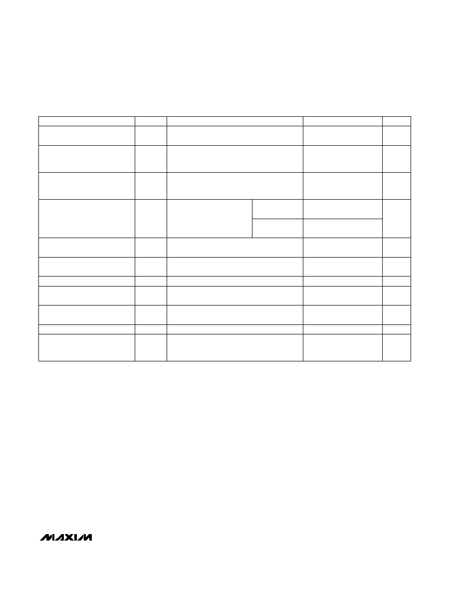
PART
MAX1661
EUB
MAX1662
EUB
MAX1663
EUB
-40∞C to +85∞C
-40∞C to +85∞C
-40∞C to +85∞C
TEMP. RANGE
PIN-PACKAGE
10 µMAX
10 µMAX
10 µMAX
EVALUATION KIT
AVAILABLE
______________Ordering Information
Typical Operating Circuits appear at end of data sheet.
SMBus is a trademark of Intel Corp.
PART
POWER-ON-
RESET STATE
INTENDED
APPLICATION
SMBus ADDRESS
ADDRESS PIN
ADDRESS
MAX1661
Outputs Low
N-Channel MOSFETs
GND
High-Z
V
CC
0100000
0111100
1001000
MAX1662
Outputs High
(high-Z state)
P-Channel MOSFETs
GND
High-Z
V
CC
0100001
0111101
1001001
MAX1663
Outputs High
(high-Z state)
P-Channel MOSFETs
GND
High-Z
V
CC
0100010
0111110
1001010
______________________________________________________________Selector Guide
Serial-to-Parallel/Parallel-to-Serial Converters and
Load-Switch Controllers with SMBus Interface

MAX1661/MAX1662/MAX1663
Serial-to-Parallel/Parallel-to-Serial Converters and
Load-Switch Controllers with SMBus Interface
2
_______________________________________________________________________________________
ABSOLUTE MAXIMUM RATINGS
ELECTRICAL CHARACTERISTICS
(V
CC
= +2.7V to +5.5V, T
A
= T
MIN
to T
MAX
, unless otherwise noted. Typical values are for T
A
= +25∞C.) (Note 1)
Stresses beyond those listed under "Absolute Maximum Ratings" may cause permanent damage to the device. These are stress ratings only, and functional
operation of the device at these or any other conditions beyond those indicated in the operational sections of the specifications is not implied. Exposure to
absolute maximum rating conditions for extended periods may affect device reliability.
V
CC
to GND ..............................................................-0.3V to +6V
I/O to GND (I/O1, I/O2, I/O3) ..................................-0.3V to +30V
I/O Sink Current (I/O1, I/O2, I/O3),
Internally Limited.............................................-1mA to +50mA
Digital Inputs to GND (SMBCLK, SMBDATA,
SMBSUS, ALERT).................................................-0.3V to +6V
ADD to GND ...............................................-0.3V to (V
CC
+ 0.3V)
SMBDATA Current, ALERT Current ....................-1mA to +50mA
Continuous Power Dissipation (T
A
= +70∞C)
10-pin µMAX (derate 5.6mW/∞C above +70∞C) ...........444mW
Operating Temperature Range
MAX166_EUB ..................................................-40∞C to +85∞C
Storage Temperature Range .............................-65∞C to +160∞C
Lead Temperature (soldering, 10sec) .............................+300∞C
V
CC
falling
Measured between the 10% level of the falling
edge and the 10% level of the rising edge
Static condition; SMBDATA, SMBCLK, ADD,
ALERT = V
CC
or GND (Note 2)
Measured between the 90% level of the rising
edge and the 90% level of the falling edge
(Notes 3, 4)
SMBCLK, SMBDATA
V
ALERT
= 5.5V, high-Z state
V
CC
= 2.7V to 5.5V;
SMBDATA, SMBCLK, SMBSUS
V
SMBDATA
, V
SMBCLK
, V
SMBSUS
,
V
ADD
= 0V, V
CC
V
ALERT
= 0.4V
V
SMBDATA
= 0.6V
V
I/O_
= 0V, V
CC
; high-impedance state
V
I/O_
= 28V, high-impedance state
V
I/O_
= 0.4V, V
CC
= 2.7V or 5.5V
V
I/O_
= 1.0V, V
CC
= 4.5V
I/O1, I/O2, or I/O3; V
CC
= 4.5V
Typical hysteresis of 10∞C
I/O_, SMBSUS, SMBCLK, SMBDATA
CONDITIONS
µs
4.7
t
LOW
SMBCLK Low Time
µs
4
t
HIGH
SMBCLK High Time
kHz
100
SMBus Clock Frequency
pF
5
SMBus Input Capacitance
µA
1
ALERT Output Leakage Current
mA
1
ALERT Output Low Sink Current
mA
6
SMBDATA Output Low Sink
Current
V
Logic Input Low Voltage
V
2.4
Logic Input High Voltage
V
1.2
1.6
2.5
Undervoltage Lockout/
Power-On Reset Threshold
µA
3
10
V
2.7
5.5
Input Voltage Range
Supply Current
V
0
5.5
SMBus Logic Input
Voltage Range
µA
-1
1
Digital Input Current
-1
0.5
1
µA
0.5
5
I/O Leakage Current
mA
2
I/O Sink Current
8
13
mA
15
20
50
I/O Current Limit
∞C
140
Thermal Shutdown
UNITS
MIN
TYP
MAX
SYMBOL
PARAMETER
0.8
I/O_, SMBSUS, SMBCLK, SMBDATA
MAX1661/MAX1662/MAX1663
Serial-to-Parallel/Parallel-to-Serial Converters and
Load-Switch Controllers with SMBus Interface
_______________________________________________________________________________________
3
Note 1:
Specifications from 0∞C to -40∞C are guaranteed by design, not production tested.
Note 2:
Supply current is specified for static state only.
Note 3:
The SMBus logic block is a static design that works with clock frequencies down to DC. While slow operation is possible, it
violates the 10kHz minimum clock frequency of the SMBus specifications, and may monopolize the bus.
Note 4:
Refer to Figures 2a and 2b for SMBus timing parameter definitions (write and read diagrams).
Note 5:
A transition must internally provide a hold time of 300ns to accommodate for the undefined region of the falling edge.
Note 6:
Refer to Figure 3 for the acknowledge timing diagram and t
DV
parameter definition.
Note 7:
Refer to Figure 5 for START-STOP interrupt timing diagrams and parameter definitions.
Note 8:
Refer to Figure 4 for I/O setup and hold timing parameter definitions.
10% or 90% of SMBDATA
to 10% of the rising edge
of SMBCLK
Measured from 90% of the rising edge
of SMBCLK to 10% of the rising edge of
SMBDATA
Measured from 10% of the falling edge
of SMBDATA to 90% of the falling edge of
SMBCLK
Measured from 90% of the SMBCLK rising
edge to 90% of the SMBDATA falling edge
CONDITIONS
ns
500
t
SU:DAT
µs
4
t
SU:STO
SMBus Stop-Condition Setup
Time
µs
4
t
HD:STA
Start-Condition Hold Time
µs
4.7
t
SU:STA
Start-Condition Setup Time
UNITS
MIN
TYP
MAX
SYMBOL
PARAMETER
Measured from 10% or 90% of V
I/O
to 10% of
the rising edge of SMBCLK (Note 8)
Measured from SMBCLK rising edge to 10%
or 90% of I/O (Note 4)
Between stop and start conditions (Note 7)
Tested with a 10k
pull-up resistor on
SMBDATA (Note 6)
(Notes 4, 5)
µs
15
t
SU:I/O
I/O Data Valid to SMBCLK
Rising-Edge Setup Time
ns
100
t
P:I/O
SMBus Write to I/O_
Propagation Delay
µs
4.7
t
BUF
SMBus Bus-Free Time
µs
1
t
DV
SMBCLK Falling Edge to
SMBus Data Valid Time
µs
0
t
HD:DAT
SMBCLK Falling Edge to
SMBDATA Transition Hold Time
Measured from the 10% point of the falling
edge of SMBDATA to the 10% point of the
rising edge of SMBDATA (Note 7)
(Note 8)
µs
10
15
30
t
LOW:SS
START-STOP Software-Interrupt
Pulse Width
µs
0
t
HD:I/O
I/O Data Hold Time
1000
SMBDATA Valid to SMBCLK
Rising Edge Time, Slave
Clocking in Data
V
CC
= 4.5V
to 5.5V
V
CC
= 2.7V
to 4.5V
ELECTRICAL CHARACTERISTICS (continued)
(V
CC
= +2.7V to +5.5V, T
A
= T
MIN
to T
MAX
, unless otherwise noted. Typical values are for T
A
= +25∞C.) (Note 1)
MAX1661/MAX1662/MAX1663
Serial-to-Parallel/Parallel-to-Serial Converters and
Load-Switch Controllers with SMBus Interface
4
_______________________________________________________________________________________
?
?W2@@@@@@@@@h?W2@@@@@@@@@
?W2@@@@@@@f@@@@@@@@@6X?g?W2@@@@@@@@@f@@@@@@@@
?W2@@@@@@@@@h?W2@@@@@@@@@?
W&@@@@@@@@@@hW&@@@@@@@@@@
W&@@@@@@@@f3@@@@@@@@@)XgW&@@@@@@@@@5f@@@@@@@@
W&@@@@@@@@@@hW&@@@@@@@@@@?
?W&@@@@@@@@@@@g?W&@@@@@@@@@@@
?W&@@@@@@@@@fV'@@@@@@@@@)X?e?W&@@@@@@@@@(Yf@@@@@@@@
?W&@@@@@@@@@@@g?W&@@@@@@@@@@@?
W&@@@@@@@@@@@@gW&@@@@@@@@@@@@
W&@@@@@@@@@@f?V'@@@@@@@@@)XeW&@@@@@@@@@(Y?f@@@@@@@@
W&@@@@@@@@@@@@gW&@@@@@@@@@@@@?
?W&@@@@@@@@@@@@@f?W&@@@@@@@@@@@@@
?W&@@@@@@@@@@@gV'@@@@@@@@@)KO&@@@@@@@@@(Yg@@@@@@@@
?W&@@@@@@@@@@@@@f?W&@@@@@@@@@@@@@?
W&@@@@@@@@@@@@@@fW&@@@@@@@@@@@@@@
W&@@@@@@@@@@@@g?V'@@@@@@@@@@@@@@@@@@@@(Y?g@@@@@@@@
?7@@@@@@@@@@@@@@fW&@@@@@@@@@@@@@@?
?W&@@@@@@@@@@@@@@@e?W&@@@@@@@@@@@@@@@
?W&@@@@@@@@@@@@@hV'@@@@@@@@@@@@@@@@@@(Yh@@@@@@@@
J@@@@@@@@@@@@@@@e?W&@@@@@@@@@@@@@@@?
W&@@@@@@@@@@@@@@@@eW&@@@@@@@@@@@@@@@@
W&@@@@@@@@@@@@@@h?V'@@@@@@@@@@@@@@@@(Y?h@@@@@@@@
?W&@@@@@@@@@@@@@@@eW&@@@@@@@@@@@@@@@@?
?W&@@@@@@@@@@@@@@@@@?W&@@@@@@@@@@@@@@@@@
?O&@@@@@@@@@@@@@@@heV'@@@@@@@@@@@@@@(Yhe@@@@@@@@
W&@@@@@@@@@@@@@@@@?W&@@@@@@@@@@@@@@@@@?
W&@@@@@@@@@@@@@@@@@@W&@@@@@@@@@@@@@@@@@@hf?W2@@@@@@@@@@@@@@@@@he?N@@@@@@@@@@@@@(Y?he@@@@@@@@hf?W&@@@@@@@@@@@@@@@@@W&@@@@@@@@@@@@@@@@@@?
?W&@@@@@@@@@@@@@@@@@@@@@@@@@@@@@@@@@@@@@@@hfW&@@@@@@@@@@@@@@@@@@hf3@@@@@@@@@@@@Hhf@@@@@@@@hfW&@@@@@@@@@@@@@@@@@@@@@@@@@@@@@@@@@@@@@@?
W&@@@@@@@@@@@@@@@@@@@@@@@@@@@@@@@@@@@@@@@@he?W&@@@@@@@@@@@@@@@@@@@hf?@@@@@@@@@@@@Lhf@@@@@@@@he?W&@@@@@@@@@@@@@@@@@@@@@@@@@@@@@@@@@@@@@@@?
?W&@@@@@@@@@@@(Y@@@@@@@@@@@@@@@@@@(Y@@@@@@@@heW&@@@@@@@@@@(M?@@@@@@@he?W&@@@@@@@@@@@@)X?he@@@@@@@@heW&@@@@@@@@@@(Y@@@@@@@@@@@@@@@@@@(Y@@@@@@@@?
W&@@@@@@@@@@@(Y?@@@@@@@@@@@@@@@@@(Y?@@@@@@@@h?W&@@@@@@@@@@(Y??@@@@@@@heW&@@@@@@@@@@@@@@)Xhe@@@@@@@@h?W&@@@@@@@@@@(Y?@@@@@@@@@@@@@@@@@(Y?@@@@@@@@?
?W&@@@@@@@@@@@(Ye@@@@@@@@@@@@@@@@(Ye@@@@@@@@hW&@@@@@@@@@@(Ye?@@@@@@@h?W&@@@@@@@@@@@@@@@@)X?h@@@@@@@@hW&@@@@@@@@@@(Ye@@@@@@@@@@@@@@@@(Ye@@@@@@@@?
W&@@@@@@@@@@@(Y?e@@@@@@@@@@@@@@@(Y?e@@@@@@@@g?W&@@@@@@@@@@(Y?eJ@@@@@@@hW&@@@@@@@@@@@@@@@@@@)Xh@@@@@@@@g?W&@@@@@@@@@@(Y?e@@@@@@@@@@@@@@@(Y?e@@@@@@@@?
?W&@@@@@@@@@@@(Yf@@@@@@@@@@@@@@(Yf@@@@@@@@gW&@@@@@@@@@@(Ye?W&@@@@@@@g?O&@@@@@@@@@@@@@@@@@@@@)X?g@@@@@@@@gW&@@@@@@@@@@(Yf@@@@@@@@@@@@@@(Yf@@@@@@@@?
W&@@@@@@@@@@@(Y?f@@@@@@@@@@@@@(Y?f@@@@@@@@f?W&@@@@@@@@@@(Y?eW&@@@@@@@@f?W2@@@@@@@@@@@@@@@@@@@@@@@)Xg@@@@@@@@f?W&@@@@@@@@@@(Y?f@@@@@@@@@@@@@(Y?f@@@@@@@@?
?W&@@@@@@@@@@@(Yg@@@@@@@@@@@@(Yg@@@@@@@@fW&@@@@@@@@@@(Ye?W&@@@@@@@@@fW&@@@@@@@@@@@0MI'@@@@@@@@@@)K?f@@@@@@@@fW&@@@@@@@@@@(Yg@@@@@@@@@@@@(Yg@@@@@@@@?
W&@@@@@@@@@@@(Y?g@@@@@@@@@@@(Y?g@@@@@@@@e?W&@@@@@@@@@@(Y?e?7@@@@@@@@@@e?W&@@@@@@@@@@(M?eV'@@@@@@@@@@@6X?e@@@@@@@@e?W&@@@@@@@@@@(Y?g@@@@@@@@@@@(Y?g@@@@@@@@?
?W&@@@@@@@@@@@(Yh@@@@@@@@@@(Yh@@@@@@@@eW&@@@@@@@@@@(YfJ@@@@@@@@@@@eW&@@@@@@@@@@(Yf?V'@@@@@@@@@@@)Xe@@@@@@@@eW&@@@@@@@@@@(Yh@@@@@@@@@@(Yh@@@@@@@@?
?7@@@@@@@@@@@(Y?h@@@@@@@@@(Y?h@@@@@@@@?W&@@@@@@@@@@(Y?e?W&@@@@@@@@@@@e7@@@@@@@@@@(Y?gV'@@@@@@@@@@@1e@@@@@@@@?W&@@@@@@@@@@(Y?h@@@@@@@@@(Y?h@@@@@@@@?
?@@@@@@@@@@@0Yhe@@@@@@@@0Yhe@@@@@@@@?&@@@@@@@@@@0Yf?&@@@@@@@@@@@@e@@@@@@@@@@0Yh?V4@@@@@@@@@@@e@@@@@@@@?&@@@@@@@@@@0Yhe@@@@@@@@0Yhe@@@@@@@@?
?
?
?W2@@@@@@@@@h?W2@@@@@@@@@
?W2@@@@@@@f@@@@@@@@@6X?g?W2@@@@@@@@@f@@@@@@@@
?W2@@@@@@@@@h?W2@@@@@@@@@?
W&@@@@@@@@@@hW&@@@@@@@@@@
W&@@@@@@@@f3@@@@@@@@@)XgW&@@@@@@@@@5f@@@@@@@@
W&@@@@@@@@@@hW&@@@@@@@@@@?
?W&@@@@@@@@@@@g?W&@@@@@@@@@@@
?W&@@@@@@@@@fV'@@@@@@@@@)X?e?W&@@@@@@@@@(Yf@@@@@@@@
?W&@@@@@@@@@@@g?W&@@@@@@@@@@@?
W&@@@@@@@@@@@@gW&@@@@@@@@@@@@
W&@@@@@@@@@@f?V'@@@@@@@@@)XeW&@@@@@@@@@(Y?f@@@@@@@@
W&@@@@@@@@@@@@gW&@@@@@@@@@@@@?
?W&@@@@@@@@@@@@@f?W&@@@@@@@@@@@@@
?W&@@@@@@@@@@@gV'@@@@@@@@@)KO&@@@@@@@@@(Yg@@@@@@@@
?W&@@@@@@@@@@@@@f?W&@@@@@@@@@@@@@?
W&@@@@@@@@@@@@@@fW&@@@@@@@@@@@@@@
W&@@@@@@@@@@@@g?V'@@@@@@@@@@@@@@@@@@@@(Y?g@@@@@@@@
?7@@@@@@@@@@@@@@fW&@@@@@@@@@@@@@@?
?W&@@@@@@@@@@@@@@@e?W&@@@@@@@@@@@@@@@
?W&@@@@@@@@@@@@@hV'@@@@@@@@@@@@@@@@@@(Yh@@@@@@@@
J@@@@@@@@@@@@@@@e?W&@@@@@@@@@@@@@@@?
W&@@@@@@@@@@@@@@@@eW&@@@@@@@@@@@@@@@@
W&@@@@@@@@@@@@@@h?V'@@@@@@@@@@@@@@@@(Y?h@@@@@@@@
?W&@@@@@@@@@@@@@@@eW&@@@@@@@@@@@@@@@@?
?W&@@@@@@@@@@@@@@@@@?W&@@@@@@@@@@@@@@@@@
?O&@@@@@@@@@@@@@@@heV'@@@@@@@@@@@@@@(Yhe@@@@@@@@
W&@@@@@@@@@@@@@@@@?W&@@@@@@@@@@@@@@@@@?
W&@@@@@@@@@@@@@@@@@@W&@@@@@@@@@@@@@@@@@@hf?W2@@@@@@@@@@@@@@@@@he?N@@@@@@@@@@@@@(Y?he@@@@@@@@hf?W&@@@@@@@@@@@@@@@@@W&@@@@@@@@@@@@@@@@@@?
?W&@@@@@@@@@@@@@@@@@@@@@@@@@@@@@@@@@@@@@@@hfW&@@@@@@@@@@@@@@@@@@hf3@@@@@@@@@@@@Hhf@@@@@@@@hfW&@@@@@@@@@@@@@@@@@@@@@@@@@@@@@@@@@@@@@@?
W&@@@@@@@@@@@@@@@@@@@@@@@@@@@@@@@@@@@@@@@@he?W&@@@@@@@@@@@@@@@@@@@hf?@@@@@@@@@@@@Lhf@@@@@@@@he?W&@@@@@@@@@@@@@@@@@@@@@@@@@@@@@@@@@@@@@@@?
?W&@@@@@@@@@@@(Y@@@@@@@@@@@@@@@@@@(Y@@@@@@@@heW&@@@@@@@@@@(M?@@@@@@@he?W&@@@@@@@@@@@@)X?he@@@@@@@@heW&@@@@@@@@@@(Y@@@@@@@@@@@@@@@@@@(Y@@@@@@@@?
W&@@@@@@@@@@@(Y?@@@@@@@@@@@@@@@@@(Y?@@@@@@@@h?W&@@@@@@@@@@(Y??@@@@@@@heW&@@@@@@@@@@@@@@)Xhe@@@@@@@@h?W&@@@@@@@@@@(Y?@@@@@@@@@@@@@@@@@(Y?@@@@@@@@?
?W&@@@@@@@@@@@(Ye@@@@@@@@@@@@@@@@(Ye@@@@@@@@hW&@@@@@@@@@@(Ye?@@@@@@@h?W&@@@@@@@@@@@@@@@@)X?h@@@@@@@@hW&@@@@@@@@@@(Ye@@@@@@@@@@@@@@@@(Ye@@@@@@@@?
W&@@@@@@@@@@@(Y?e@@@@@@@@@@@@@@@(Y?e@@@@@@@@g?W&@@@@@@@@@@(Y?eJ@@@@@@@hW&@@@@@@@@@@@@@@@@@@)Xh@@@@@@@@g?W&@@@@@@@@@@(Y?e@@@@@@@@@@@@@@@(Y?e@@@@@@@@?
?W&@@@@@@@@@@@(Yf@@@@@@@@@@@@@@(Yf@@@@@@@@gW&@@@@@@@@@@(Ye?W&@@@@@@@g?O&@@@@@@@@@@@@@@@@@@@@)X?g@@@@@@@@gW&@@@@@@@@@@(Yf@@@@@@@@@@@@@@(Yf@@@@@@@@?
W&@@@@@@@@@@@(Y?f@@@@@@@@@@@@@(Y?f@@@@@@@@f?W&@@@@@@@@@@(Y?eW&@@@@@@@@f?W2@@@@@@@@@@@@@@@@@@@@@@@)Xg@@@@@@@@f?W&@@@@@@@@@@(Y?f@@@@@@@@@@@@@(Y?f@@@@@@@@?
?W&@@@@@@@@@@@(Yg@@@@@@@@@@@@(Yg@@@@@@@@fW&@@@@@@@@@@(Ye?W&@@@@@@@@@fW&@@@@@@@@@@@0MI'@@@@@@@@@@)K?f@@@@@@@@fW&@@@@@@@@@@(Yg@@@@@@@@@@@@(Yg@@@@@@@@?
W&@@@@@@@@@@@(Y?g@@@@@@@@@@@(Y?g@@@@@@@@e?W&@@@@@@@@@@(Y?e?7@@@@@@@@@@e?W&@@@@@@@@@@(M?eV'@@@@@@@@@@@6X?e@@@@@@@@e?W&@@@@@@@@@@(Y?g@@@@@@@@@@@(Y?g@@@@@@@@?
?W&@@@@@@@@@@@(Yh@@@@@@@@@@(Yh@@@@@@@@eW&@@@@@@@@@@(YfJ@@@@@@@@@@@eW&@@@@@@@@@@(Yf?V'@@@@@@@@@@@)Xe@@@@@@@@eW&@@@@@@@@@@(Yh@@@@@@@@@@(Yh@@@@@@@@?
?7@@@@@@@@@@@(Y?h@@@@@@@@@(Y?h@@@@@@@@?W&@@@@@@@@@@(Y?e?W&@@@@@@@@@@@e7@@@@@@@@@@(Y?gV'@@@@@@@@@@@1e@@@@@@@@?W&@@@@@@@@@@(Y?h@@@@@@@@@(Y?h@@@@@@@@?
?@@@@@@@@@@@0Yhe@@@@@@@@0Yhe@@@@@@@@?&@@@@@@@@@@0Yf?&@@@@@@@@@@@@e@@@@@@@@@@0Yh?V4@@@@@@@@@@@e@@@@@@@@?&@@@@@@@@@@0Yhe@@@@@@@@0Yhe@@@@@@@@?
?
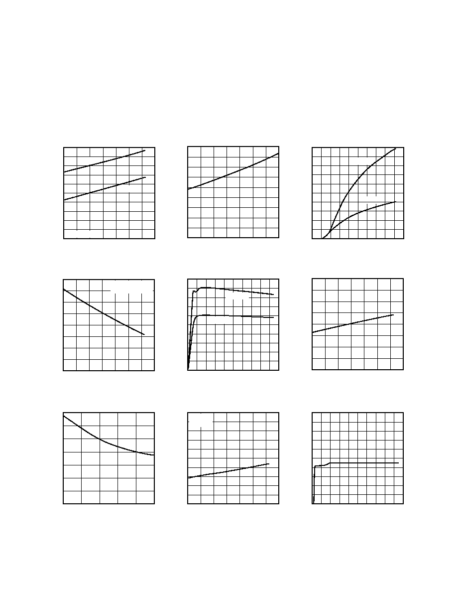
__________________________________________Typical Operating Characteristics
(V
CC
= +5.0V, T
A
= +25∞C, unless otherwise noted.)
0
3.0
1.5
7.5
9.0
6.0
4.5
10.5
15.0
13.5
12.0
0
1.2 1.8
0.6
2.4 3.0 3.6 4.2 4.8 5.4 6.0
I/O_ SINK CURRENT
vs. SUPPLY VOLTAGE
MAX1661toc01
SUPPLY VOLTAGE (V)
SINK CURRENT (mA)
V
I/O_
= 1.0V
V
I/O_
= 0.4V
0
1.0
0.5
2.5
2.0
1.5
4.0
3.5
3.0
4.5
2.0
3.0
3.5
2.5
4.0
4.5
5.0
5.5
SUPPLY CURRENT vs. SUPPLY VOLTAGE
MAX1661toc02
SUPPLY VOLTAGE (V)
SUPPLY CURRENT (
µ
A)
0
1.5
1.0
0.5
2.5
2.0
4.5
4.0
3.5
3.0
5.0
-40
-20
0
20
40
60
80
100
SUPPLY CURRENT
vs. TEMPERATURE
MAX1661toc03
TEMPERATURE (∞C)
SUPPLY CURRENT (
µ
A)
V
CC
= 5.5V
V
CC
= 2.7V
ALL I/Os OFF
10
12
14
16
18
20
22
24
26
-40
40
20
0
-20
60
80
100
I/O_ CURRENT LIMIT
vs. TEMPERATURE
MAX1661toc04
TEMPERATURE (∞C)
CURRENT LIMIT (mA)
V
I/O_
FORCED TO 15V
V
CC
= 5.5V
0
10
5
20
15
30
25
35
3.0
4.0
4.5
3.5
5.0
5.5
POR DELAY vs. SUPPLY VOLTAGE
MAX1661toc07
SUPPLY VOLTAGE (V)
POR DELAY (
µ
s)
0
5.0
2.5
12.5
10.0
7.5
15.0
17.5
25.0
22.5
20.0
0
6
9
3
12 15 18 21 24 27
30
I/O_ CURRENT LIMIT vs. I/O_ VOLTAGE
MAX1661toc05
V
I/O_
(V)
CURRENT LIMIT (mA)
V
CC
= 2.7V
V
CC
= 5.5V
0
5
10
15
20
25
30
35
40
-40
40
20
0
-20
60
80
100
POR DELAY vs. TEMPERATURE
MAX1661toc06
TEMPERATURE (∞C)
POR DELAY (
µ
s)
0
0.3
0.2
0.1
0.5
0.4
0.9
0.8
0.7
0.6
1.0
-40
-20
0
20
40
60
80
100
I/O_ INPUT BIAS CURRENT
vs. TEMPERATURE
MAX1661toc08
TEMPERATURE (∞C)
INPUT BIAS CURRENT (
µ
A)
V
CC
= 5.5V
V
I/O_
= 15V
0
0.2
0.1
0.5
0.4
0.3
0.6
0.7
1.0
0.9
0.8
0
6
9
3
12 15 18 21 24 27
30
I/O_INPUT BIAS CURRENT
vs. OUTPUT VOLTAGE
MAX1661toc09
OUTPUT VOLTAGE (V)
INPUT BIAS CURRENT (
µ
A)

MAX1661/MAX1662/MAX1663
Serial-to-Parallel/Parallel-to-Serial Converters and
Load-Switch Controllers with SMBus Interface
_______________________________________________________________________________________
5
______________________________________________________________Pin Description
NAME
FUNCTION
1
V
CC
Supply Voltage Input, 2.7V to 5.5V.
2
I/O1
Input 1 or Output 1 (open drain). This pin can tolerate up to 28V.
PIN
3
I/O2
Input 2 or Output 2 (open drain). This pin can tolerate up to 28V.
4
I/O3
Input 3 or Output 3 (open drain). This pin can tolerate up to 28V.
8
SMBDATA
SMBus Serial-Data Input/Output (open drain)
7
SMBSUS
SMBus Suspend-Mode Control Input. Drive low to select the suspend-mode register. Drive high to select
the normal-mode register. (See
Detailed Description.)
6
ADD
SMBus Address Select Pin (see Table 1 for details).
5
GND
Ground
10
ALERT
Interrupt Output, active low, open drain
9
SMBCLK
SMBus Serial Clock Input
INPUT
REGISTER
TRANSITION
DETECTORS
SMBSUS
NORMAL
DATA
REGISTER
NORMAL
I/01
I/02
I/03
SUSPEND
O1
CONTROL
NORMAL
SUSPEND
CONTROL
NORMAL
SUSPEND
CONTROL
SUSPEND-
MODE
DATA
REGISTER
ALERT
RESPONSE
REGISTER
ADDRESS
DECODER
SMB
THERMAL
SHUTDOWN
8
7
ALERT
FAULT
LATCH
S
R
ADD
SMBDATA
SMBCLK
MAX1661/
MAX1662/
MAX1663
O2
O3
MUX
MUX
MUX
Figure 1. Functional Diagram