 | ÐлекÑÑоннÑй компоненÑ: MAX1665V | СкаÑаÑÑ:  PDF PDF  ZIP ZIP |
Äîêóìåíòàöèÿ è îïèñàíèÿ www.docs.chipfind.ru
For free samples and the latest literature visit www.maxim-ic.com or phone 1-800-998-8800.
For small orders, phone 1-800-835-8769.
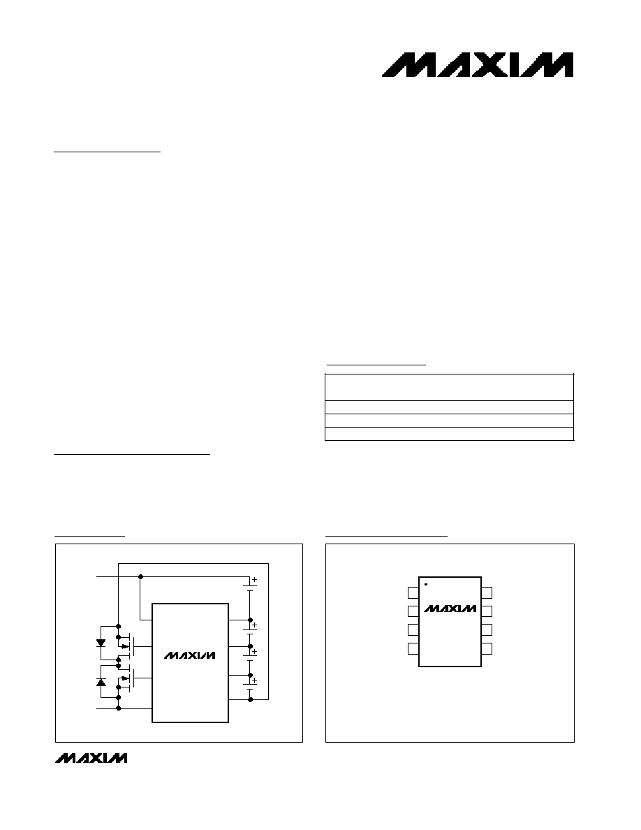
General Description
The MAX1665 provides protection against overvoltage,
undervoltage, overcharge current, and overdischarge
current for 2-cell to 4-cell lithium-ion (Li+) battery packs.
Very low operating current ensures that cells are not
overdischarged during long storage periods.
The MAX1665 controls two external N-channel MOSFETs
to limit the charge and discharge voltages. Charging is
allowed when the per-cell voltage is below +4.3V. When
the voltage on any cell rises above +4.3V (overvoltage
limit), the MAX1665 turns off the charge MOSFET. This
safety feature prevents overcharge of any cell within the
battery pack.
Discharge is allowed when the per-cell voltage is above
+2.5V (undervoltage limit). If the voltage across any cell
falls below +2.5V, the MAX1665 turns off the discharge
MOSFET. This safety feature prevents overdischarge of
any cell within the battery pack.
Charging and discharging are allowed if the voltage
between PKN and BN is less than 250mV. This safety fea-
ture prevents excessive pack current.
Applications
Lithium-Ion Battery Packs
____________________________Features
o Complete Protection Against:
Cell Overvoltage
Cell Undervoltage
o Pack Protection for Excessive Charge and
Discharge
o Very Low Supply Current: 16µA typ
o Low Standby Current: 1µA max
o Matched Cell Input Bias Current (<500pA)
Preserves Cell Balance
MAX1665S/V/X
Lithium-Ion Battery Pack Protector
________________________________________________________________ Maxim Integrated Products
1
B1P
PKN
BN
1
2
8
7
I.C. [B3P]
B2P
DSG
CHG
I.C. (B4P)
NOTES: I.C. = INTERNAL CONNECTION. MAKE NO CONNECTIONS TO THIS PIN.
( ) ARE FOR THE MAX1665X.
[ ] ARE FOR THE MAX1665V AND MAX1665X.
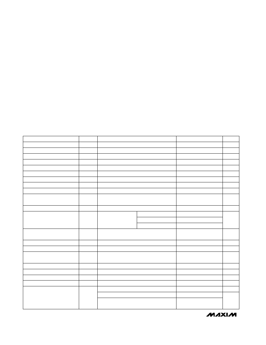
SO
TOP VIEW
3
4
6
5
MAX1665S
MAX1665V
MAX1665X
MAX1665X
B4P
B3P
DSG
B2P
B1P
PKN
(-)
(+)
CHG
BN
Typical Operating Circuit
19-1605; Rev 0; 1/00
Pin Configuration
Ordering Information
PART
MAX1665SESA
MAX1665VESA
MAX1665XESA
-40°C to +85°C
-40°C to +85°C
-40°C to +85°C
TEMP. RANGE
PIN-
PACKAGE
8 SO
8 SO
8 SO
CELL
COUNT
2
3
4
MAX1665S/V/X
Lithium-Ion Battery Pack Protector
2
_______________________________________________________________________________________
ABSOLUTE MAXIMUM RATINGS
ELECTRICAL CHARACTERISTICS
(V
B2P
= 8V (MAX1665S), V
B3P
= 12V (MAX1665V), V
B4P
= 16V (MAX1665X), T
A
= 0°C to +85°C, unless otherwise noted. Typical
values are at T
A
= +25°C.)
Stresses beyond those listed under "Absolute Maximum Ratings" may cause permanent damage to the device. These are stress ratings only, and functional
operation of the device at these or any other conditions beyond those indicated in the operational sections of the specifications is not implied. Exposure to
absolute maximum rating conditions for extended periods may affect device reliability.
B4P to PKN (MAX1665X)........................................-0.3V to +24V
B3P to PKN (MAX1665V)........................................-0.3V to +18V
B2P to PKN (MAX1665S)........................................-0.3V to +12V
B1P to PKN, B2P to B1P, B3P to B2P, B4P to B3P...-0.3V to +6V
CHG to PKN, DSG to BN
MAX1665S............................................-0.3V to (V
B2P
+ 0.3V)
MAX1665V............................................-0.3V to (V
B3P
+ 0.3V)
MAX1665X............................................-0.3V to (V
B4P
+ 0.3V)
B2P to BN (MAX1665S)..........................................-0.3V to +12V
B3P to BN (MAX1665V)..........................................-0.3V to +18V
B4P to BN (MAX1665X)..........................................-0.3V to +24V
Continuous Power Dissipation (T
A
= +70°C)
8-Pin SO (derate 5.88mW/°C above +70°C)...............471mW
Operating Temperature Range ...........................-40°C to +85°C
Junction Temperature ......................................................+150°C
Temperature Range...........................................-65°C to +150°C
Lead Temperature (soldering, 10s) .................................+300°C
MAX1665SESA, V
B1P
= 4V
nA
3
10
MAX1665X
MAX1665V
MAX1665S
V
PKN
= ±300mV
V
PKN
= ±300mV
(Note 1)
V
CHG
= V
PKN
+ 3.0V
CHG = PKN, DSG = BN
Cell voltage rising
I
DSG
= -1µA
V
BN
- V
PKN
MAX1665X, I
OUT
= 100µA, V
B4P
= 24V,
V
BN
= 100mV
CONDITIONS
I
BIAS
Input Bias Current (Note 3)
MAX1665VESA, V
B1P
= 4V, V
B2P
= 8V
nA
3
10
MAX1665XESA, V
B1P
= 4V, V
B2P
= 8V,
V
B3P
= 12V
3
10
ms
135
t
OFF
Overcurrent Sampling - t
OFF
ms
8.2
t
ON
Overcurrent Sampling - t
ON
mA
0.5
2
I
OL
CHG Output Sink Current
mA
10
25
I
OH
CHG, DSG Output Source
Current
V
V
BN
+ 0.1
V
DSGL
DSG Output Voltage Low
V
17
20
DSG Output Voltage High
(Note 2)
V
4
20
V
B4P
B4P Voltage Range
V
4 15
V
B3P
V
4
10
V
B2P
B2P Voltage Range
B3P Voltage Range
ms
10
t
IO
Overcurrent Detection Delay
ms
200
t
UV
Overvoltage/Undervoltage
Delay
mV
5
V
CH2
Overcurrent Hysteresis
mV
±200
±250
±300
V
CH
Overcurrent Sense Threshold
V
4.26
4.3
4.34
V
OV
Overvoltage Threshold
V
0.10
V
CE
Overvoltage Hysteresis
V
2.4
2.5
2.6
V
UV
Undervoltage Threshold
mV
0
18
30
V
RE
Undervoltage RESET
UNITS
MIN
TYP
MAX
SYMBOL
PARAMETER
I
OUT
= 100µA
V
V
B2P
- 1.8
V
B2P
- 0.54
CHG, DSG Output Voltage High
I
CHG
= -100µA
V
V
B3P
- 1.8
V
B3P
- 0.54
MAX1665S
MAX1665V
V
PKN
+ 0.1
V
CHGL
V
B4P
- 1.8
V
B4P
- 0.54
MAX1665X
CHG Output Voltage Low
V
DSG
= V
BN
+ 3.0V
µA
0.5
2
I
OL
DSG Output Sink Current
MAX1665S/V/X
Lithium-Ion Battery Pack Protector
_______________________________________________________________________________________
3
ELECTRICAL CHARACTERISTICS (continued)
(V
B2P
= 8V (MAX1665S), V
B3P
= 12V (MAX1665V), V
B4P
= 16V (MAX1665X), T
A
= 0°C to +85°C, unless otherwise noted. Typical
values are at T
A
= +25°C.)
ELECTRICAL CHARACTERISTICS
(V
B2P
= 8V (MAX1665S), V
B3P
= 12V (MAX1665V), V
B4P
= 16V (MAX1665X), T
A
= -40°C to +85°C, unless otherwise noted.) (Note 6)
Note 1: Applies to the differential voltage measured on any cell.
Note 2: DSG is internally clamped to a maximum of 20V to protect the external MOSFET (V
GS
).
Note 3: Guaranteed by design.
Note 4: The input bias matching between cells is measured with a 4V voltage between cells.
Note 5: At least one cell is <V
UV
.
Note 6: Specifications to -40°C are guaranteed by design, not production tested.
MAX1665SESA, V
B1P
= 4V
nA
10
MAX1665X
DSG = CHG = low
MAX1665V
MAX1665S
V
DSG
= V
BN
+ 0.3V
V
CHG
= V
PKN
+ 0.3V
CHG = PKN, DSG = BN
Cell voltage rising
I
DSG
= -1µA
V
BN
- V
PKN
MAX1665X, I
OUT
= 100µA, V
B4P
= 24V,
V
BN
= 100mV
CONDITIONS
I
BIAS
Input Bias Current (Note 3)
MAX1665VESA, V
B1P
= 4V, V
B2P
= 8V
10
MAX1665XESA, V
B1P
= 4V, V
B2P
= 8V,
V
B3P
= 12V
10
V
4.7
V
UVLO
Undervoltage Lockout
µA
30
I
CC
Supply Current
µA
0.2
I
OL
DSG Output Sink Current
mA
0.2
I
OL
CHG Output Sink Current
mA
10
I
OH
CHG, DSG Output Source
Current
V
V
BN
+ 0.1
V
DSGL
DSG Output Voltage Low
V
20
DSG Output Voltage High
(Note 2)
V
4
20
V
B4P
B4P Voltage Range
V
4 15
V
B3P
V
4
10
V
B2P
B2P Voltage Range
B3P Voltage Range
mV
±180
±320
V
CH
Overcurrent Sense Threshold
V
4.20
4.24
V
OV
Overvoltage Threshold
V
2.4
2.6
V
UV
Undervoltage Threshold
mV
0
30
V
RE
Undervoltage RESET
UNITS
MIN
TYP
MAX
SYMBOL
PARAMETER
I
OUT
= 100µA
V
V
B2P
- 2
V
B2P
- 0.5
CHG, DSG Output Voltage High
I
CHG
= -100µA
V
V
B3P
- 2
V
B3P
- 0.5
MAX1665S
MAX1665V
V
PKN
+ 0.1
V
CHGL
V
B4P
- 2
V
B4P
- 0.5
MAX1665X
CHG Output Voltage Low
(Note 5)
µA
2
I
LP
Standby Mode Current
DSG = CHG = low
(Note 5)
CONDITIONS
(Notes 3, 4)
pA
±500
I
BIAS
V
4.0
4.7
V
UVLO
Undervoltage Lockout
µA
0.7
1
I
LP
Standby Mode Current
µA
16
25
I
CC
Supply Current
UNITS
MIN
TYP
MAX
SYMBOL
PARAMETER
Input Bias Current Matching
MAX1665S/V/X
Lithium-Ion Battery Pack Protector
4
_______________________________________________________________________________________
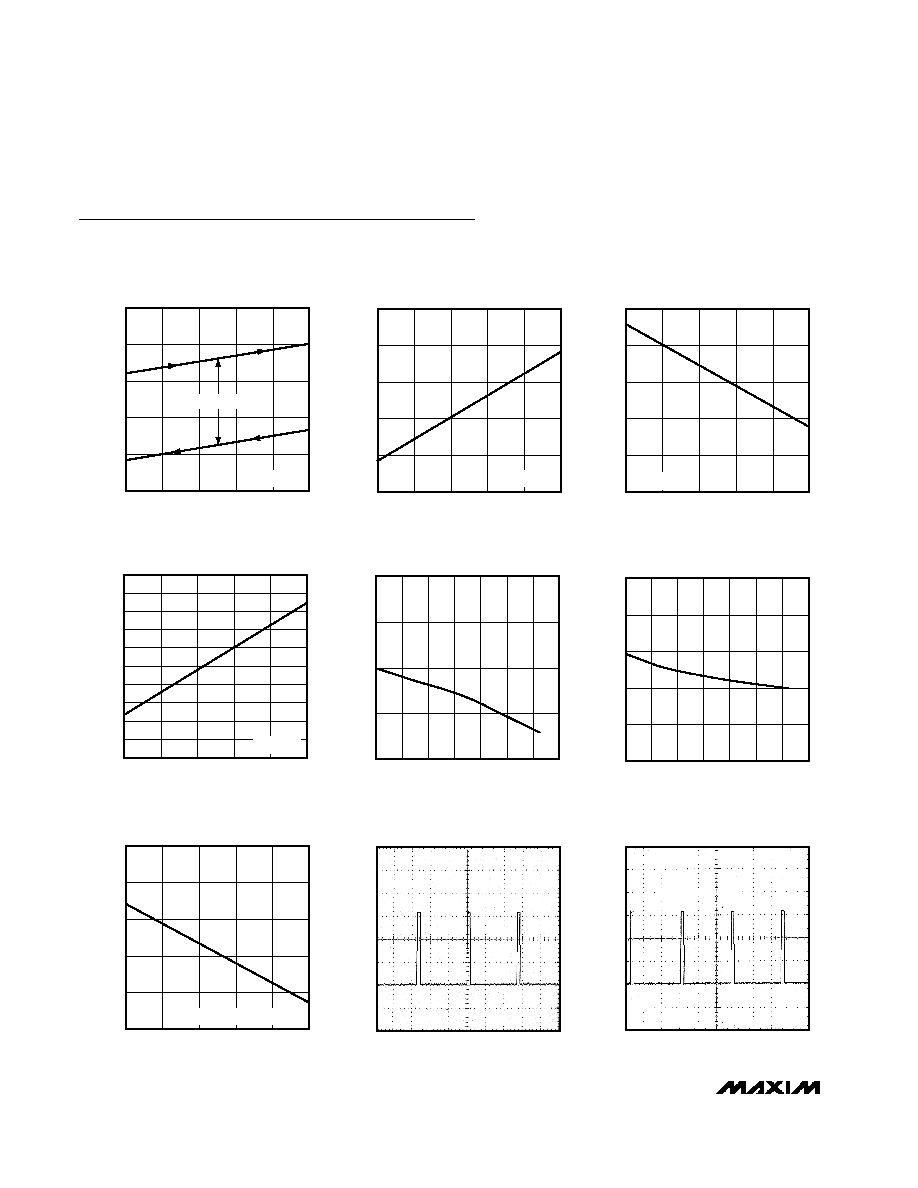
Typical Operating Characteristics
(T
A
= +25°C, unless otherwise noted.)
4.14
4.18
4.26
4.22
4.30
4.34
-40
10
-15
35
60
85
OVERVOLTAGE THRESHOLD vs.
TEMPERATURE
MAX1665 toc01
TEMPERATURE (°C)
THRESHOLD VOLTAGE (V)
V
BN
- V
PKN
HYSTERESIS
2.46
2.47
2.49
2.48
2.50
2.51
-40
10
-15
35
60
85
UNDERVOLTAGE THRESHOLD vs.
TEMPERATURE
MAX1665 toc02
TEMPERATURE (°C)
UNDERVOLTAGE THRESHOLD (V)
V
BN
- V
PKN
240
243
249
246
252
255
-40
10
-15
35
60
85
OVERCURRENT THRESHOLD vs.
TEMPERATURE
MAX1665 toc03
TEMPERATURE (°C)
OVERCURRENT THRESHOLD (mV)
V
BN
- V
PKN
-260
-254
-256
-258
-252
-250
-248
-246
-244
-242
-240
-40
10
-15
35
60
85
OVERDISCHARGE THRESHOLD
vs. TEMPERATURE
MAX1665 toc04
TEMPERATURE (°C)
OVERDISCHARGE THRESHOLD (mV)
V
BN -
V
PKN
16.0
16.4
17.2
16.8
17.6
18.0
2.5
3.5
3.0
4.0
4.5
5.0
QUIESCENT CURRENT
vs. SUPPLY VOLTAGE
MAX1665 toc07
SUPPLY VOLTAGE PER CELL (V)
QUIESCENT CURRENT (
µ
A)
NORMALIZED TO ONE CELL
16.0
16.5
17.0
17.5
18.0
SUPPLY CURRENT
vs. TEMPERATURE
MAX1665 toc05
TEMPERATURE (°C)
SUPPLY CURRENT (
µ
A)
-40
20
40
-20
0
60
80
100
0.5
0.6
0.8
0.7
0.9
1.0
-40
0
-20
20
40
60
80
100
STANDBY MODE CURRENT
vs. TEMPERATURE
MAX1665 toc06
TEMPERATURE (°C)
STANDBY CURRENT (
µ
A)
CHG
2V/div
50ms/div
CONTINUOUS OVERCHARGE CONDITION
MAX1665 toc08
DSG
2V/div
50ms/div
CONTINUOUS OVERDISCHARGE CONDITION
MAX1665 toc09
MAX1665S/V/X
Lithium-Ion Battery Pack Protector
_______________________________________________________________________________________
5
FUNCTION
1, 8
1
Internally Connected. Make no connection to this pin.
--
--
Cell 4 Positive Input. Connect to the positive terminal of the fourth
series Li+ cell.
2
2
Discharge Control Output. Drives the gate of an external N-channel
MOSFET to control the discharge path.
3
3
Charge Control Output. Drives the gate of an external N-channel
MOSFET to control the charge path.
7
7
Cell 2 Positive Input. Connect to the positive terminal of the second
series Li+ cell.
6
6
Cell 1 Positive Input. Connect to the positive terminal of the first
series Li+ cell.
5
5
Connect to the negative terminal of the first series Li+ cell.
4
4
Pack Negative Input
--
8
Cell 3 Positive Input. Connect to the positive terminal of the third
series Li+ cell.
Pin Description
--
1
2
3
7
6
5
4
8
NAME
I.C.
B4P
DSG
CHG
B2P
B1P
BN
PKN
B3P
MAX1665V
MAX1665S
MAX1665X
PIN
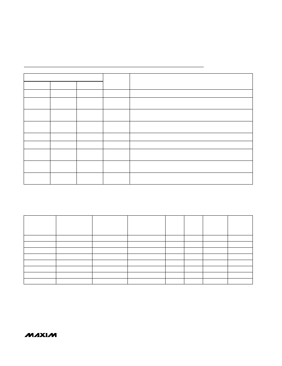
Table 1. Functionality Truth Table for V
BN
< V
PKN
+ 0.018V (Discharge Mode)
*Assuming no load on CHG or DSG.
0
1
1
1
1
25
Yes
No
Low
Gated
Low
Low
1
1
0
0
1
0
1
1
0
0
1
25
1
No
Yes
No
Low
Gated
Low
Low
Gated
Low
0
1
1
0
0
0
UNDERVOLTAGE
0
1
0
OVERVOLTAGE
0
0
1
25
1
25
MAX
SUPPLY
CURRENT*
(µA)
GATE
CLOCKED
No
No
No
High
Low
High
DSG
Low
Low
High
CHG
DISCHARGE
OVERCURRENT
0
0
0
0
0
0
CHARGE
OVERCURRENT