 | ÐлекÑÑоннÑй компоненÑ: MAX16806 | СкаÑаÑÑ:  PDF PDF  ZIP ZIP |
Äîêóìåíòàöèÿ è îïèñàíèÿ www.docs.chipfind.ru
General Description
The MAX16805/MAX16806 LED drivers eliminate the
need for microcontrollers or switch-mode converters for
automotive interior dome, map, and courtesy light
applications. An EEPROM-programmable LED current-
sense reference simplifies production by using one
sense resistor to set the LED current for all LED bins. A
dual-mode DIM pin and an on-board 200Hz ramp gen-
erator allow for PWM dimming with an analog or PWM
control signal. The analog control signal at dimming
input DIM allows for the "theater dimming" effect to be
implemented. Fast turn-on/-off times ensure a wide-
range PWM operation, while waveshaping circuitry min-
imizes EMI. EEPROM-programmable LED current
foldback makes it possible to operate at a high input
voltage, while saving the cost and space associated
with having a large heatsink. The MAX16806 works with
an external thermal sensor to maintain maximum LED
junction temperature by folding back the LED current.
The thermal foldback temperature knee and slope are
EEPROM programmable. The MAX16806 SW pin sup-
plies necessary wetting current to a momentary switch.
Applications
Automotive Interior: Map, Dome, and Courtesy
Lighting
Automotive Exterior:
Rear Combination Light (RCL)
Daytime Running Light (DRL)
Adaptive Front Light
Emergency Vehicle Warning Lights
Navigation and Marine Indicators
Features
o EEPROM or I
2
C* Dynamically Programmable:
LED Current Foldback for High Input Voltage
LED Current Reference
LED Current Thermal Foldback (MAX16806)
o On-Board 200Hz Ramp Generator Eliminates the
Need for µC PWM Signal
o Flexible Analog or PWM Control for PWM or
Theater Dimming
o Wetting Current and Debounce for Momentary
Switch (MAX16806)
o 5.5V to 40V Input with Up to 39V Output Capability
o 35mA to 350mA Adjustable LED Current
o Waveshaping Minimizes EMI During Dimming
o Output Short-Circuit and Overtemperature
Protection
o -40°C to +125°C Operating Temperature Range
MAX16805/MAX16806
EEPROM-Programmable, High-Voltage, 350mA
LED Drivers with LED Current Foldback
________________________________________________________________
Maxim Integrated Products
1
Ordering Information
19-0625; Rev 0; 8/06
For pricing, delivery, and ordering information, please contact Maxim/Dallas Direct! at
1-888-629-4642, or visit Maxim's website at www.maxim-ic.com.
*
Purchase of I
2
C components from Maxim Integrated Products,
Inc. or one of its sublicensed Associated Companies, conveys
a license under the Philips I
2
C Patent Rights to use these com-
ponents in an I
2
C system, provided that the system conforms
to the I
2
C Standard Specification as defined by Philips.
Pin Configurations appear at end of data sheet.
+
Denotes lead-free package.
**
EP = Exposed pad.
PART
TEMP RANGE
PIN
PACKAGE
PKG
CODE
MAX16805ATP+ -40°C to +125°C 20 TQFN-EP** T2055M-5
MAX16806ATP+ -40°C to +125°C 20 TQFN-EP** T2055M-5
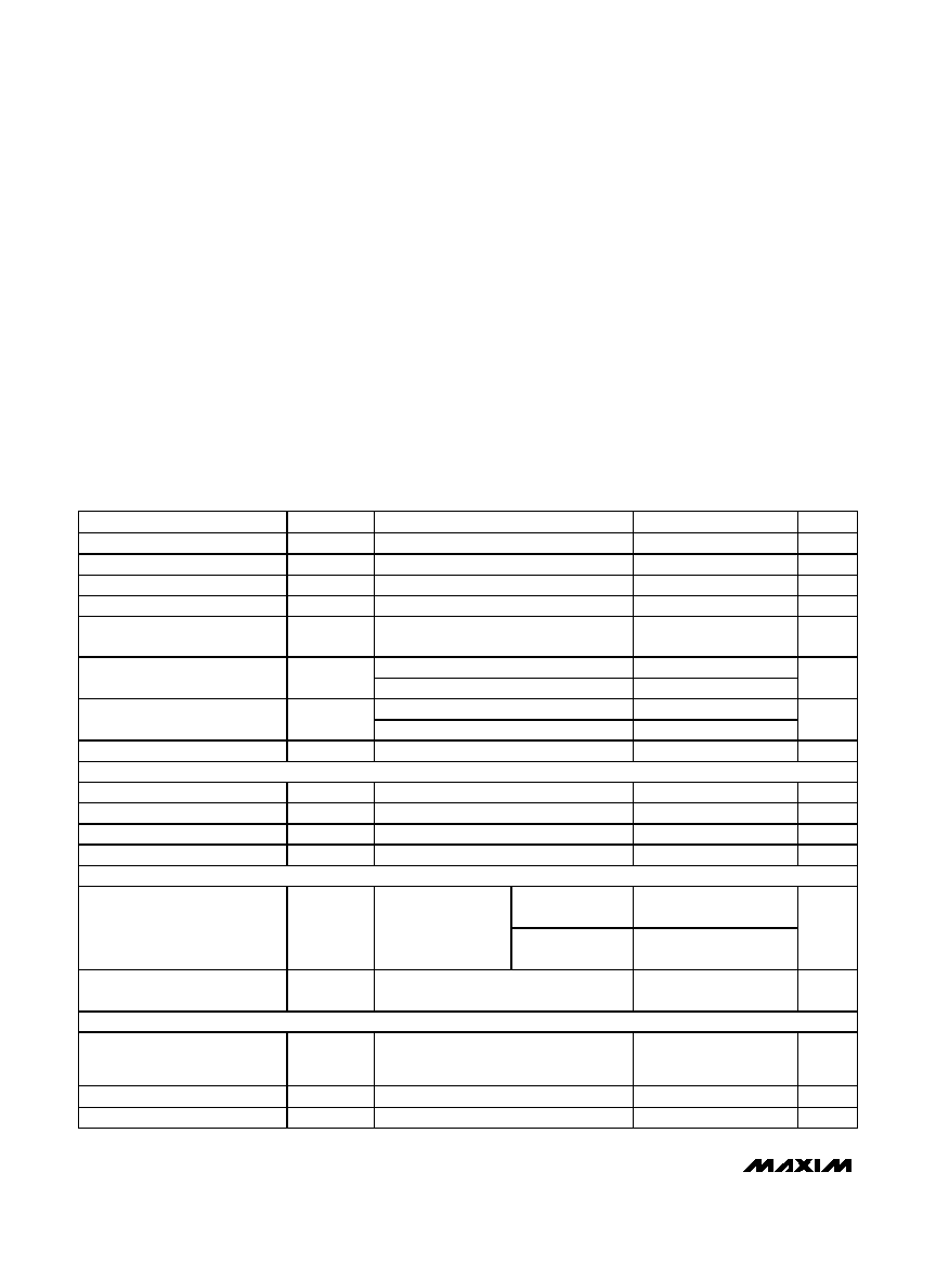
MAX16805
IN
OUT
V5
LEDs
I
LED
R
SENSE
0.1
µF
+5.5V TO +40V
+5V REG
CS+
0.1
µF
CS-
DIM
GND
EN
V5
ANALOG CONTROL PWM DIMMING
SCL
SDA
SERIAL CLOCK
SERIAL DATA
I
LED
MAX16806
MAX6613
IN
OUT
V5
LEDs
R
SENSE
0.1
µF
+5.5V TO +40V
PWM CONTROL DIMMING
+5V REG
CS+
0.1
µF
CS-
DIM
PWM DIMMING
GND
EN
TFP/SCL
TFN/SDA
V
CC
V5
GND
OUT
SW
MAX6613 THERMAL SENSOR IS OPTIONAL.
Typical Operating Circuits
MAX16805/MAX16806
EEPROM-Programmable, High-Voltage, 350mA
LED Drivers with LED Current Foldback
2
_______________________________________________________________________________________
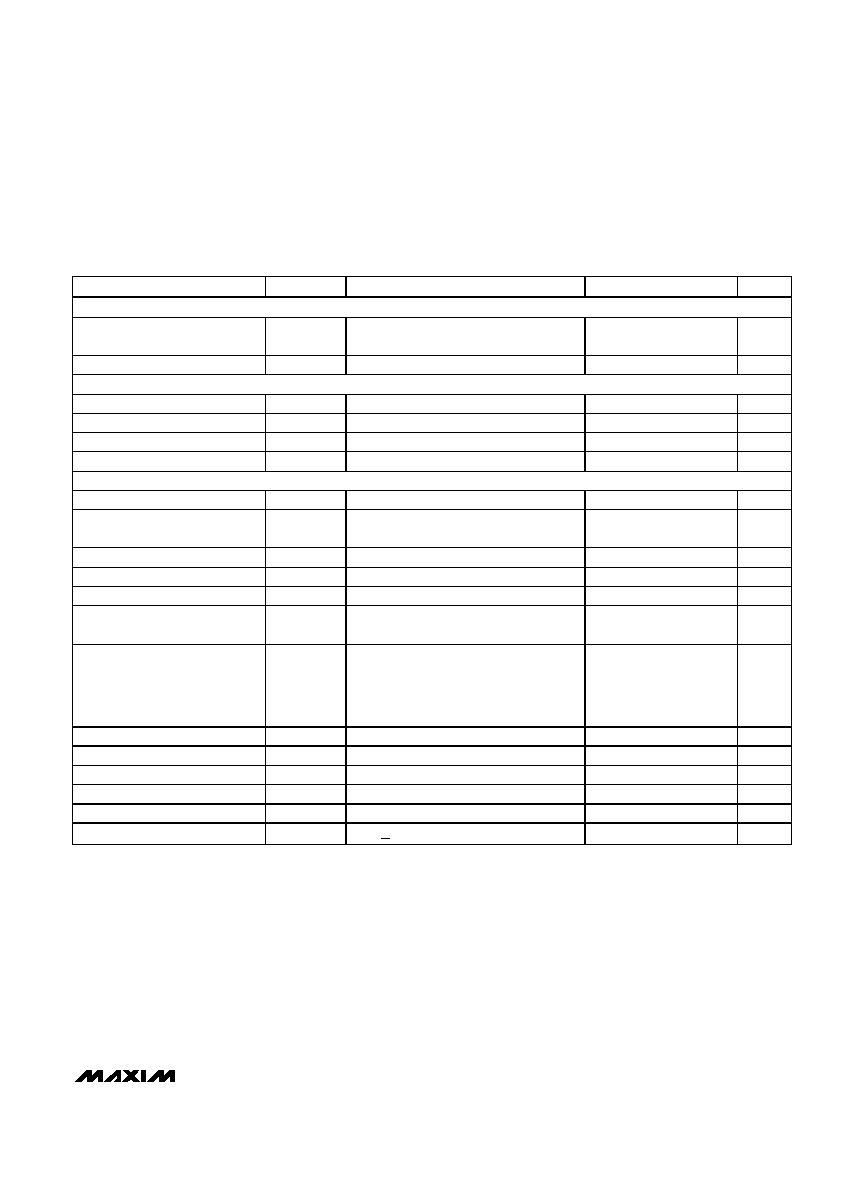
ABSOLUTE MAXIMUM RATINGS
ELECTRICAL CHARACTERISTICS
(V
IN
= V
EN
= 12V, C
V5
= 0.1µF, I
V5
= 0, CS- = GND, R
SENSE
= 0.56, V
DIM
= 4V, DGND = GND, TFP/SCL = 5V, TFN/SDA = 0V,
SW = CFD = Open, T
A
= T
J
= -40°C to +125°C, unless otherwise noted. Typical values are at T
A
= +25°C.) (Note 1)
Stresses beyond those listed under "Absolute Maximum Ratings" may cause permanent damage to the device. These are stress ratings only, and functional
operation of the device at these or any other conditions beyond those indicated in the operational sections of the specifications is not implied. Exposure to
absolute maximum rating conditions for extended periods may affect device reliability.
IN to GND ...............................................................-0.3V to +45V
DIM, OUT, EN to GND ................................-0.3V to (V
IN
+ 0.3V)
IN Slew Rate (20V < V
IN
< 45V) ...................................250mV/µs
SDA, SCL (MAX16805), TFN/SDA,
TFP/SCL (MAX16806) to GND...............................-0.3V to +6V
CFD, CS+, V5 to GND ..............................................-0.3V to +6V
DGND and CS- to GND.........................................-0.3V to +0.3V
OUT Short Circuited to GND Duration (V
IN
< +16V)..........1 hour
Maximum Current Into Any Pin (except IN and OUT) ......±20mA
Continuous Power Dissipation (T
A
= +70°C)
20-Pin Thin QFN (derate 34.5mW/°C above +70°C)....2758.6mW
Operating Temperature Range .........................-40°C to +125°C
Junction Temperature ......................................................+150°C
Storage Temperature Range .............................-65°C to +150°C
Lead Temperature (soldering, 10s) .................................+300°C
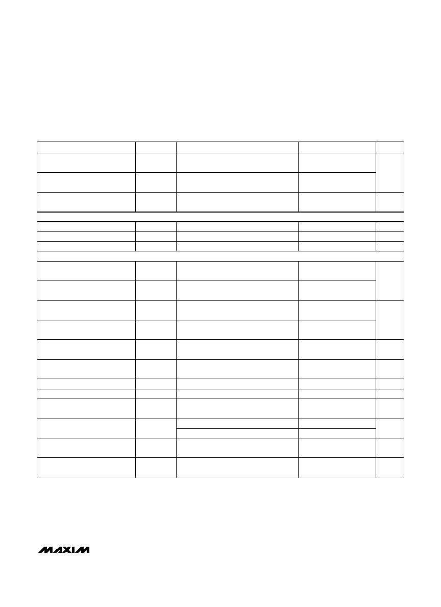
PARAMETER
SYMBOL
CONDITIONS
MIN
TYP
MAX
UNITS
Supply Voltage Range
V
IN
(Note 2)
5.5
40
V
Ground Current
I
G
I
LOAD
= 350mA
2.5
4.5
mA
Shutdown Supply Current
I
SHDN
V
EN
0.3V
12
40
µA
Guaranteed Output Current
I
OUT
R
SENSE
= 0.55
350
mA
Output Current Accuracy
35mA < I
OUT
< 350mA, R
SENSE
tolerance
not included
3.0
%
I
OUT
= 350mA, 12V < V
IN
< 40V
0.4
1.2
Dropout Voltage (Note 3)
V
DO
I
OUT
= 350mA, 6.5V < V
IN
< 12V
0.5
1.5
V
Current rising, DIM rising to 4V
17
Output Current Slew Rate
(External PWM Signal at DIM)
Current falling, DIM falling to 0.6V
17
mA/µs
Short-Circuit Current
V
OUT
= 0V
600
mA
ENABLE INPUT
EN Input Current
I
EN
100
nA
EN Input-Voltage High
V
IH
2.8
V
EN Input-Voltage Low
V
IL
0.6
V
Enable Turn-On Time
t
ON
EN rising edge to 90% of OUT
225
µs
5V REGULATOR
0 < I
V5
< 0.5mA,
SW = GND
4.9
5.1
5.3
Output Voltage Regulation
(MAX16806)
V5
6.5V < V
IN
< 40V
0 < I
V5
< 2mA,
SW = open
4.9
5.1
5.3
V
Output Voltage Regulation
(MAX16805)
V5
0 < I
V5
< 2mA, 6.5V < V
IN
< 40V
4.9
5.1
5.3
V
CURRENT SENSE
Regulated R
SENSE
Voltage
V
RSNS
V
SENSE
= [V
CS+
- V
CS-
], Binning
Adjustment register at factory default
(0x0F)
192
198
204
mV
Input Current (CS+)
V
CS+
= 210mV
12
µA
Input Current (CS-)
V
CS+
= 210mV
-75
µA
MAX16805/MAX16806
EEPROM-Programmable, High-Voltage, 350mA
LED Drivers with LED Current Foldback
_______________________________________________________________________________________
3
PARAMETER
SYMBOL
CONDITIONS
MIN
TYP
MAX
UNITS
Minimum Regulated V
SENSE
Programming Range
V
SENSE(MIN)
99.4
103
106.6
Maximum Regulated V
SENSE
Programming Range
V
SENSE(MAX)
192
198
204
mV
Regulated V
SENSE
Default
Voltage
V
SENSE(DEF)
Binning Adjustment register at factory
default (0x0F)
198
mV
EXTERNAL PWM DIMMING INPUT
DIM Input Current
0.5
µA
Turn-On Time
t
ON
After DIM rising to 4V (Note 4)
28
52
µs
Turn-Off Time
t
OFF
After DIM falling to 0.6V (Note 4)
19
38
µs
THERMAL FOLDBACK (MAX16806 with MAX6613)
Maximum Thermal Foldback
Knee Point Programming Range
TF
KNEE(MAX)
326
335
354
Minimum Thermal Foldback Knee
Point Programming Range
TF
KNEE(MIN)
1143
1174
1213
mV
M i ni m um Ther m al Fol d b ack
Tem p er atur e P r og r am m i ng Rang e
TF
( M I N )
+ 60
M axi m um Ther m al Fol d b ack
Tem p er atur e P r og r am m i ng Rang e
TF
(MAX)
+135
° C
Thermal Foldback Default
Threshold Temperature
V
TH
Thermal Foldback Knee Point register at
factory default (0x00)
+60
°C
Thermal Foldback Default
Threshold Voltage
TF
VTH
1.174
V
M i ni m um Ther m al Fol d b ack S l op e
TF
SL(MIN)
3.88
4
4.12
V/V
M axi m um Ther m al Fol d b ack S l op e
TF
SL(MAX)
15.52
16
16.48
V/V
Thermal Foldback Default Slope
Thermal Foldback Slope Gain register at
factory default (0x03)
4
V/V
I
2
C interface active
-0.3
V5
TFP/SCL (SCL for MAX16805)
Voltage Compliance Range
V
TFP
Remote thermal sensor active
+0.3
V5
V
TFN/SDA (SDA for MAX16805)
Voltage Compliance Range
V
TFN
-0.3
V5
V
Minimum Thermal Foldback
Clamp Current Reduction Range
TF
C(MIN)
+25
o
C
T
A
+125
o
C
40
%
ELECTRICAL CHARACTERISTICS (continued)
(V
IN
= V
EN
= 12V, C
V5
= 0.1µF, I
V5
= 0, CS- = GND, R
SENSE
= 0.56, V
DIM
= 4V, DGND = GND, TFP/SCL = 5V, TFN/SDA = 0V,
SW = CFD = Open, T
A
= T
J
= -40°C to +125°C, unless otherwise noted. Typical values are at T
A
= +25°C.) (Note 1)
MAX16805/MAX16806
EEPROM-Programmable, High-Voltage, 350mA
LED Drivers with LED Current Foldback
4
_______________________________________________________________________________________
ELECTRICAL CHARACTERISTICS (continued)
(V
IN
= V
EN
= 12V, C
V5
= 0.1µF, I
V5
= 0, CS- = GND, R
SENSE
= 0.56, V
DIM
= 4V, DGND = GND, TFP/SCL = 5V, TFN/SDA = 0V,
SW = CFD = Open, T
A
= T
J
= -40°C to +125°C, unless otherwise noted. Typical values are at T
A
= +25°C.) (Note 1)
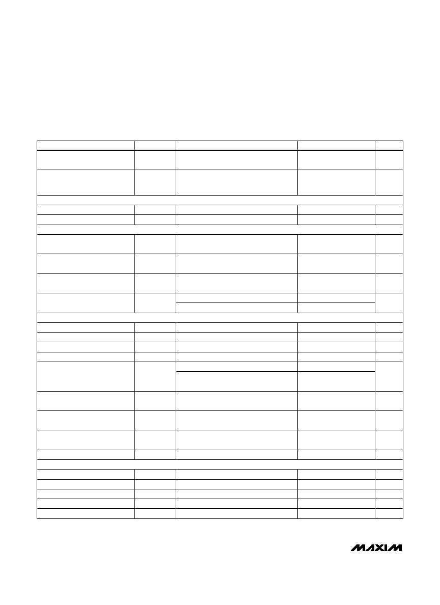
PARAMETER
SYMBOL
CONDITIONS
MIN
TYP
MAX
UNITS
Maximum Thermal Foldback
Clamp Current Reduction Range
TF
C(MAX)
+25
o
C
T
A
+125
o
C
100
%
Default Thermal Foldback Clamp
Current Reduction Range
TF
DEF
Thermal Foldback Clamp register at
factory default (0x07),
+25
o
C
T
A
+125
o
C
40
%
THERMAL PROTECTION
Thermal Shutdown Temperature
T
J(SHDN)
+155
°C
Thermal Shutdown Hysteresis
+23
°C
LED CURRENT FOLDBACK
Minimum Input LED Current
Foldback Range
V
CFD(MIN)
11.4
V
Maximum Input LED Current
Foldback Range
V
CFD(MAX)
16.4
V
LED Current Foldback Default
Level
V
CFD
LED Current Foldback Threshold register
at factory default (0x00)
16.4
V
V
IN
> 11V, CFD register bit 3 = 0
0.71
LED Current Foldback Voltage
Step Size
V
IN
> 11V, CFD register bit 3 = 1
0.355
V/step
INTERNAL RAMP GENERATOR
Internal RAMP Frequency
f
RAMP
176
200
224
Hz
External Sync Frequency Range
f
DIM
80
2000
Hz
External Sync Voltage Low
0.4
V
External Sync Voltage High
2.8
V
V
DIM
= 0V
0
Output Current Duty Cycle
I
DC
V
DIM
> (V
RAMP
+ 0.4V) (MAX16806),
V
DIM
> +3.3V (MAX16805)
100
%
Minimum Ramp Peak
Programming Range
V
RAMP(MIN)
1.49
1.55
1.60
V
Maximum Ramp Peak
Programming Range
V
RAMP(MAX)
2.77
2.88
3.00
V
Ramp Peak Default Voltage
Ramp Peak register at factory default
(0x07)
2.88
V
Ramp Offset Voltage
210
mV
MOMENTARY SWITCH INTERFACE (SW) (MAX16806)
SW Pullup Current
I
SW
V
SW
= 0V
1
3
mA
SW Input-Voltage High
V
IH
I
SW
= 100µA
4
V
SW Input-Voltage Low
V
IL
0.4
V
Minimum Pulse Width
120
ms
Minimum Debounce Time
40
ms
MAX16805/MAX16806
EEPROM-Programmable, High-Voltage, 350mA
LED Drivers with LED Current Foldback
_______________________________________________________________________________________
5
ELECTRICAL CHARACTERISTICS (continued)
(V
IN
= V
EN
= 12V, C
V5
= 0.1µF, I
V5
= 0, CS- = GND, R
SENSE
= 0.56, V
DIM
= 4V, DGND = GND, TFP/SCL = 5V, TFN/SDA = 0V,
SW = CFD = Open, T
A
= T
J
= -40°C to +125°C, unless otherwise noted. Typical values are at T
A
= +25°C.) (Note 1)
PARAMETER
SYMBOL
CONDITIONS
MIN
TYP
MAX
UNITS
EEPROM
V
IN
Voltage for EEPROM
Programming
20
22
24
V
EEPROM Data-Retention Time
10
Years
I
2
C DIGITAL INPUTS (TFP/SCL, TFN/SDA) (Note 5)
Logic Input-Voltage High
V
IH
2.8
V
Logic Input-Voltage Low
V
IL
0.8
V
Input Capacitance
5
pF
SDA Output Voltage Low
V
OL
I
SINK
= 3mA
0.4
V
I
2
C INTERFACE TIMING (Figure 1)
Serial Clock Frequency
f
SCL
400
kHz
Bus Free Time Between STOP
and START Condition
t
BUF
1.3
µs
START Condition Hold Time
t
HD:STA
0.6
µs
Clock Low Period
t
LOW
1.3
µs
Clock High Period
t
HIGH
0.6
µs
Repeat START Condition Setup
Time
t
SU:STA
0.6
µs
Data Hold Time
t
HD:DAT
A master device must provide a hold time
of at least 300ns for the SDA signal
(referred to V
IL
of the SCL signal) in order
to bridge the undefined region of SCL's
falling edge
0
0.9
µs
Data Setup Time
t
SU:DAT
100
ns
Receive SCL/SDA Rise Time
t
R
300
ns
Receive SCL/SDA Fall Time
t
F
250
ns
STOP Condition Setup Time
t
SU:STO
0.6
µs
Pulse Width of Spike Suppressed
t
SP
50
ns
Transmit SDA Fall Time
I
SINK
<
6mA, C
B
400pF (Note 6)
250
ns
Note 1: All devices 100% production tested at T
J
= +25°C. Limits over the operating temperature range are guaranteed by design.
Note 2: Resistors were added from OUT to CS+ to aid with the power dissipation during testing.
Note 3: Dropout is measured as follows: Connect a resistor from OUT to CS+. Connect R
SENSE
= 0.56 from CS+ to CS-. Set V
IN
=
V
OUT
+3V (record V
OUT
as V
OUT1
). Reduce V
IN
until V
OUT
= 0.97 x V
OUT1
(record as V
IN2
and V
OUT2
). V
DO
= V
IN2
- V
OUT2
.
Note 4: t
ON
time includes the delay and the rise time needed for I
OUT
to reach 90% of its final value. t
OFF
time is the time needed for
I
OUT
to drop below 10%. See the
Typical Operating Characteristics. t
ON
and t
OFF
are tested with 13 from OUT to CS+.
Note 5: TPF/SCL (SCL for MAX16805) and TPN/SDA (SDA for the MAX16805) are I
2
C interface compatible only when the
MAX16805/MAX16806 are the only parts on the bus for production programming.
Note 6: C
B
is the total bus capacitance.