 | ÐлекÑÑоннÑй компоненÑ: MAX1697 | СкаÑаÑÑ:  PDF PDF  ZIP ZIP |
Äîêóìåíòàöèÿ è îïèñàíèÿ www.docs.chipfind.ru
General Description
The MAX1697 ultra-small, monolithic, CMOS charge-
pump voltage inverter accepts an input voltage ranging
from +1.25V to +5.5V. This device features an ultra-low
12
output resistance, permitting loads of up to 60mA
with maximum efficiency. The MAX1697 is available
with operating frequencies of 12kHz, 35kHz, 125kHz, or
250kHz, allowing optimization of supply current or
external component size. Its small external components
and micropower shutdown mode make this device
ideal for both battery-powered and board-level voltage
conversion applications.
Oscillator control circuitry and four power MOSFET
switches are included on-chip. Applications include
generating a negative supply from a +5V or +3.3V logic
supply to power analog circuitry. All versions come in a
6-pin SOT23 package and deliver 60mA.
For applications with lower current requirements, the
MAX1719/MAX1720/MAX1721 are pin-compatible
SOT23 charge pumps that supply up to 25mA.
Applications
Negative Supply from +5V or +3.3V Logic Supplies
Small LCD Panels
GaAsFET Bias Supplies
Handy-Terminals, PDAs
Battery-Operated Equipment
Features
60mA Output Current
Low 12
Output Resistance
150µA Supply Current (MAX1697R)
Requires Only Two 1µF Capacitors (MAX1697U)
Start-Up Current Limited
+1.25V to +5.5V Input Voltage Range
0.1µA Logic-Controlled Shutdown
Slew-Rate Limited to Reduce EMI
6-Pin SOT23 Package
MAX1697
60mA, SOT23 Inverting Charge Pump
with Shutdown
________________________________________________________________
Maxim Integrated Products
1
SHDN
5
TOP VIEW
IN
GND
C1-
C1+
OUT
SOT23-6
1
6
MAX1697
2
3
4
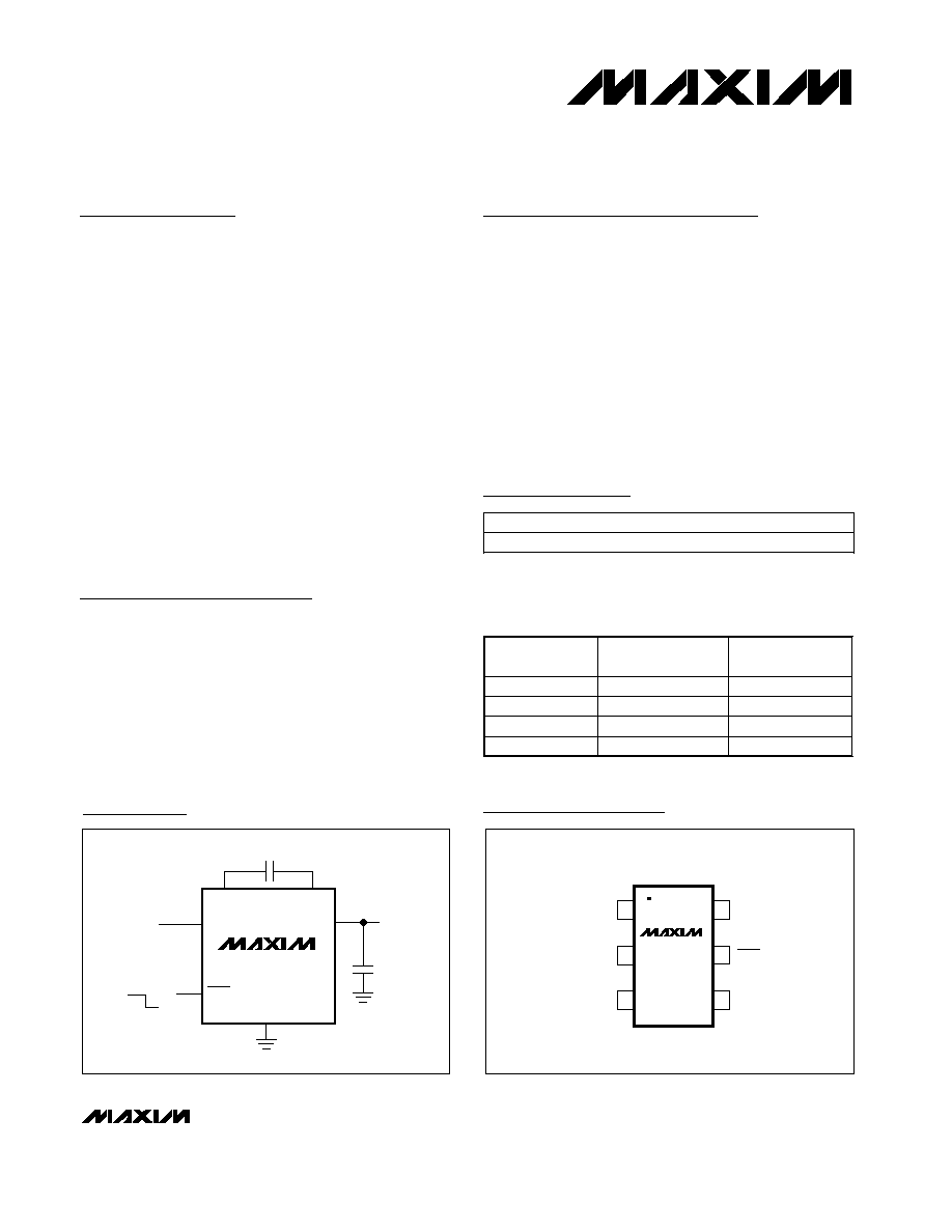
Pin Configuration
C1+
C1-
IN
SHDN
OUT
GND
ON
1
µ
F
1
µ
F
OFF
INPUT
1.5V to 5.5V
NEGATIVE
OUTPUT
-1
·
V
IN
60mA
MAX1697U
Typical Operating Circuit
19-1499; Rev 0; 7/99
PART
MAX1697
_
EUT-T
-40°C to +85°C
TEMP. RANGE
PIN-PACKAGE
6 SOT23-6
Ordering Information
For free samples & the latest literature: http://www.maxim-ic.com, or phone 1-800-998-8800.
For small orders, phone 1-800-835-8769.
PART NO.
SUFFIX
R
12
FREQUENCY
(kHz)
TOP
MARK
AABV
S
35
AABW
T
U
250
AABY
125
AABX
Note:
The MAX1697 is available with four different operating
frequencies. Choose the desired frequency from the table
below and insert the suffix in the blank above to complete the
part number.
MAX1697
60mA, SOT23 Inverting Charge Pump
with Shutdown
2
_______________________________________________________________________________________
ABSOLUTE MAXIMUM RATINGS
ELECTRICAL CHARACTERISTICS
(Circuit of Figure 1, capacitors from Table 2, V
IN
= +5V, SHDN = IN,
T
A
= 0°C to +85°C
, unless otherwise noted. Typical values are at
T
A
= +25°C.)
Stresses beyond those listed under "Absolute Maximum Ratings" may cause permanent damage to the device. These are stress ratings only, and functional
operation of the device at these or any other conditions beyond those indicated in the operational sections of the specifications is not implied. Exposure to
absolute maximum rating conditions for extended periods may affect device reliability.
IN to GND .................................................................-0.3V to +6V
C1+, SHDN to GND .....................................-0.3V to (V
IN
+ 0.3V)
C1- to GND ..............................................(V
OUT
- 0.3V) to + 0.3V
OUT to GND .............................................................+0.3V to -6V
OUT Output Current............................................................90mA
OUT Short-Circuit to GND .............................................Indefinite
Continuous Power Dissipation (T
A
= +70°C)
6-Pin SOT23 (derate 14mW/°C above +70°C) ................1.1W
Operating Temperature Range ...........................-40°C to +85°C
Junction Temperature ......................................................+150°C
Storage Temperature Range .............................-65°C to +150°C
Lead Temperature (soldering, 10sec) .............................+300°C
I
OUT
= 15mA
MAX1697T/U, R
L
= 5k
SHDN = GND or IN
V
IN(MIN)
V
IN
2.5V
MAX1697R/S, R
L
= 5k
2.5V
V
IN
5.5V
V
IN(MIN)
V
IN
2.5V
2.5V
V
IN
5.5V
I
OUT
= 0, T
A
= +25°C
SHDN = GND, OUT is internally pulled to GND
in shutdown
T
A
= +25°C
T
A
= +25°C
SHDN = GND
I
OUT
= 60mA
CONDITIONS
600
µs
1200
Wake-Up Time from Shutdown
10
nA
-100
0.05
+100
SHDN Bias Current
0.2
V
0.6
SHDN Input Logic Low
V
IN
- 0.2
V
2.0
SHDN Input Logic High
3
8
OUT to GND Shutdown
Resistance
33
12
25
Output Resistance (Note 1)
1.4
5.5
1.5
5.5
V
1.25
5.5
Supply Voltage Range
%
99
99.9
Voltage Conversion Efficiency
20
35
50
kHz
Oscillator Frequency
0.03
1.5
5.5
µA
150
300
Quiescent Supply Current
350
650
µA
0.002
1
Shutdown Supply Current
UNITS
MIN
TYP
MAX
PARAMETER
T
A
= 0°C to + 85°C
T
A
= +25°C
T
A
= 0°C to + 85°C
T
A
= +25°C
MAX1697S
MAX1697R
T
A
= +85°C
T
A
= +25°C
T
A
= 0°C to +85°C
T
A
= +25°C
T
A
= +85°C
T
A
= +25°C
MAX1697S
MAX1697R
MAX1697U
MAX1697T
950
1700
1800
3400
Output shorted to ground, T
A
= +25°C
mA
170
Short-Circuit Current
7
12
17
MAX1697U
70
MAX1697T
100
140
250
360
70
125
180
MAX1697R
MAX1697S
MAX1697T
MAX1697U
MAX1697
60mA, SOT23 Inverting Charge Pump
with Shutdown
_______________________________________________________________________________________
3
ELECTRICAL CHARACTERISTICS
(Circuit of Figure 1, capacitors from Table 2, V
IN
= +5V, SHDN = IN,
T
A
= -40°C to +85°C
, unless otherwise noted.) (Note 2)
ELECTRICAL CHARACTERISTICS (continued)
(Circuit of Figure 1, capacitors from Table 2, V
IN
= +5V, SHDN = IN,
T
A
= 0°C to +85°C
, unless otherwise noted. )Typical values are at
T
A
= +25°C.)
CONDITIONS
150
UNITS
MIN
TYP
MAX
PARAMETER
Note 1:
Output resistance is guaranteed with capacitor ESR of 0.3
or less.
Note 2:
All specifications from -40°C to +85°C are guaranteed by design, not production tested.
Trip Temperature
°C
Hysteresis
°C
15
Temperature increasing
THERMAL SHUTDOWN
V
R
L
= 5k
Supply Voltage Range
1.6
5.5
MAX1697R
V
IN(MIN)
V
IN
2.5V
2.5V
V
IN
5.5V
V
IN(MIN)
V
IN
2.5V
2.5V
V
IN
5.5V
MAX1697T/U
1.5
5.5
µA
SHDN = GND, OUT is internally pulled to GND in
shutdown
350
Continuous, long-term
Quiescent Current
750
MAX1697T
MAX1697R
I
OUT
= 60mA
CONDITIONS
1800
kHz
6
21
3600
MAX1697S
MAX1697U
Oscillator Frequency
16
60
MAX1697T
60
200
120
400
MAX1697S
MAX1697U
MAX1697R/S
0.2
V
0.6
SHDN Input Logic Low
V
IN
- 0.2
V
2.1
SHDN Input Logic High
8
OUT to GND Shutdown
Resistance
33
Output Resistance (Note 1)
mA
RMS
60
Output Current
UNITS
MIN
MAX
PARAMETER
0
10
15
25
20
30
1.5
2.5
3.0
2.0
3.5
4.0
4.5
5.0
5.5
MAX1697R/S/T/U
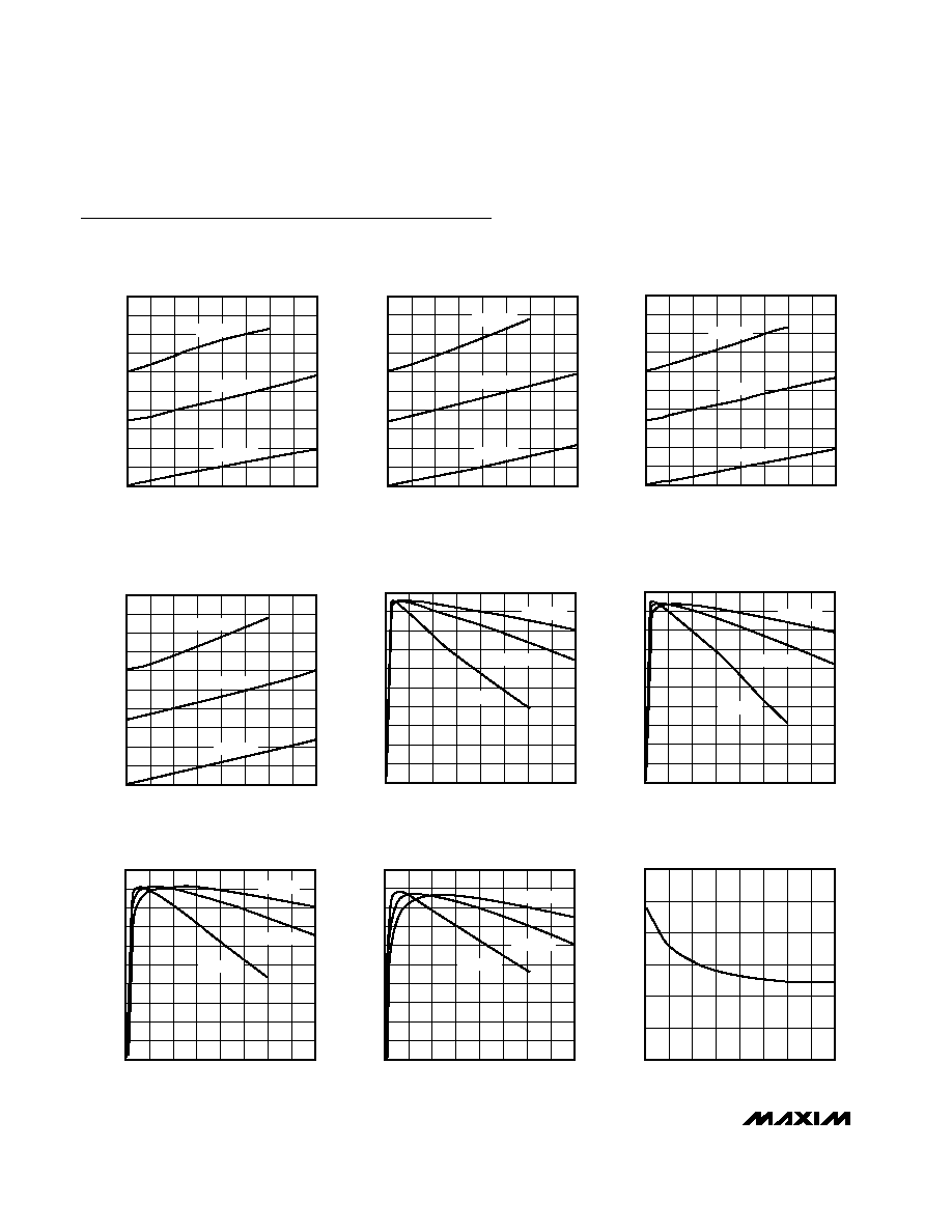
OUTPUT IMPEDANCE vs. INPUT VOLTAGE
MAX1697 TOC09
INPUT VOLTAGE (V)
OUTPUT IMPEDANCE (
)
5
0
20
10
40
30
60
50
70
90
80
100
0
20
30
10
40
50
60
70
80
MAX1697U
EFFICIENCY vs. OUTPUT CURRENT
MAX1697 TOC08
OUTPUT CURRENT (mA)
EFFICIENCY (%)
V
IN
= +2V
V
IN
= +5V
V
IN
= +3.3V
MAX1697
4
_______________________________________________________________________________________
0
20
10
40
30
60
50
70
90
80
100
0
20
30
10
40
50
60
70
80
MAX1697T
EFFICIENCY vs. OUTPUT CURRENT
MAX1697 TOC07
OUTPUT CURRENT (mA)
EFFICIENCY (%)
V
IN
= +2V
V
IN
= +5V
V
IN
= +3.3V
-5.0
-4.0
-4.5
-3.0
-3.5
-2.0
-2.5
-1.5
-0.5
-1.0
0
0
20
30
10
40
50
60
70
80
MAX1697R
OUTPUT VOLTAGE
vs. OUTPUT CURRENT
MAX1697 TOC01
OUTPUT CURRENT (mA)
OUTPUT VOLTAGE (V)
V
IN
= +2V
V
IN
= +5V
V
IN
= +3.3V
-5.0
-4.0
-4.5
-3.0
-3.5
-2.0
-2.5
-1.5
-0.5
-1.0
0
0
20
30
10
40
50
60
70
80
MAX1697U
OUTPUT VOLTAGE
vs. OUTPUT CURRENT
MAX1697 TOC04
OUTPUT CURRENT (mA)
OUTPUT VOLTAGE (V)
V
IN
= +2V
V
IN
= +5V
V
IN
= +3.3V
-5.0
-4.0
-4.5
-3.0
-3.5
-2.0
-2.5
-1.5
-0.5
-1.0
0
0
20
30
10
40
50
60
70
80
MAX1697S
OUTPUT VOLTAGE
vs. OUTPUT CURRENT
MAX1697 TOC02
OUTPUT CURRENT (mA)
OUTPUT VOLTAGE (V)
V
IN
= +2V
V
IN
= +5V
V
IN
= +3.3V
-5.0
-4.0
-4.5
-3.0
-3.5
-2.0
-2.5
-1.5
-0.5
-1.0
0
0
20
30
10
40
50
60
70
80
MAX1697T
OUTPUT VOLTAGE
vs. OUTPUT CURRENT
MAX1697 TOC03
OUTPUT CURRENT (mA)
OUTPUT VOLTAGE (V)
V
IN
= +2V
V
IN
= +5V
V
IN
= +3.3V
0
20
10
40
30
60
50
70
90
80
100
0
20
30
10
40
50
60
70
80
MAX1697R
EFFICIENCY vs. OUTPUT CURRENT
MAX1697 TOC05
OUTPUT CURRENT (mA)
EFFICIENCY (%)
V
IN
= +2V
V
IN
= +5V
V
IN
= +3.3V
0
20
10
40
30
60
50
70
90
80
100
0
20
30
10
40
50
60
70
80
MAX1697S
EFFICIENCY vs. OUTPUT CURRENT
MAX1697 TOC06
OUTPUT CURRENT (mA)
EFFICIENCY (%)
V
IN
= +2V
V
IN
= +5V
V
IN
= +3.3V
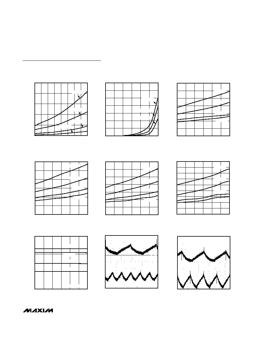
Typical Operating Characteristics
(Circuit of Figure 1, capacitors from Table 2, V
IN
= +5V, SHDN = IN, T
A
= +25°C, unless otherwise noted.)
60mA, SOT23 Inverting Charge Pump
with Shutdown
MAX1697
60mA, SOT23 Inverting Charge Pump
with Shutdown
_______________________________________________________________________________________
5
0
0.5
1.0
2.0
1.5
2.5
1.5
2.5
3.0
2.0
3.5
4.0
4.5
5.0
5.5
SUPPLY CURRENT
vs. INPUT VOLTAGE
MAX1697 TOC10
INPUT VOLTAGE (V)
SUPPLY CURRENT (mA)
MAX1697R
MAX1697S
MAX1697T
MAX1697U
0
5
15
10
25
20
30
35
-40
0
20
-20
40
60
80
MAX1697R/S/T/U
SHUTDOWN SUPPLY CURRENT
vs. TEMPERATURE
MAX1697 TOC11
TEMPERATURE (°C)
SUPPLY CURRENT (nA)
V
IN
= +2V
V
IN
= +3.3V
V
IN
= +5V
0
5
15
10
25
20
30
35
-40
0
20
-20
40
60
80
MAX1697R
OUTPUT RESISTANCE
vs. TEMPERATURE
MAX1697 TOC12
TEMPERATURE (°C)
OUTPUT RESISTANCE (
)
V
IN
= +2V
V
IN
= +1.5V
V
IN
= +5V
V
IN
= +3.3V
0
5
15
10
25
20
30
-40
0
20
-20
40
60
80
MAX1697S
OUTPUT RESISTANCE
vs. TEMPERATURE
MAX1697 TOC13
TEMPERATURE (°C)
OUTPUT RESISTANCE (
)
V
IN
= +2V
V
IN
= +1.5V
V
IN
= +5V
V
IN
= +3.3V
1
100
10
1000
-40
-20
0
20
40
60
80
PUMP FREQUENCY
vs. TEMPERATURE
MAX1697 TOC16
TEMPERATURE (°C)
PUMP FREQUENCY (kHz)
MAX1697U
MAX1697T
MAX1697S
MAX1697R
V
IN
= +1.5V TO +5V
0
5
15
10
25
20
30
35
-40
0
20
-20
40
60
80
MAX1697T
OUTPUT RESISTANCE
vs. TEMPERATURE
MAX1697 TOC14
TEMPERATURE (°C)
OUTPUT RESISTANCE (
)
V
IN
= +2V
V
IN
= +1.5V
V
IN
= +5V
V
IN
= +3.3V
0
5
15
10
25
20
30
40
35
45
-40
0
20
-20
40
60
80
MAX1697U
OUTPUT RESISTANCE
vs. TEMPERATURE
MAX1697 TOC15
TEMPERATURE (°C)
OUTPUT RESISTANCE (
)
V
IN
= +2V
V
IN
= +1.5V
V
IN
= +5V
V
IN
= +3.3V
V
OUT
MAX1697R
(12kHz)
V
OUT
MAX1697S
(35kHz)
MAX1697R/S
OUTPUT NOISE AND RIPPLE
MAX1697 TOC17
20
µ
s/div
V
IN
= 3.3V, I
OUT
= 5mA,
10mV/div, AC-COUPLED
V
OUT
MAX1697T
(125kHz)
V
OUT
MAX1697U
(250kHz)
MAX1697T/U
OUTPUT NOISE AND RIPPLE
MAX1697 TOC18
2
µ
s/div
V
IN
= 3.3V, I
OUT
= 5mA,
10mV/div, AC-COUPLED
Typical Operating Characteristics (continued)
(Circuit of Figure 1, capacitors from Table 2, V
IN
= +5V, SHDN = IN, T
A
= +25°C, unless otherwise noted.)