 | –≠–ª–µ–∫—Ç—Ä–æ–Ω–Ω—ã–π –∫–æ–º–ø–æ–Ω–µ–Ω—Ç: MAX1711 | –°–∫–∞—á–∞—Ç—å:  PDF PDF  ZIP ZIP |

For free samples & the latest literature: http://www.maxim-ic.com, or phone 1-800-998-8800
For small orders, phone 1-800-835-8769.
General Description
The MAX1710/MAX1711 step-down controllers are
intended for core CPU DC-DC converters in notebook
computers. They feature a triple-threat combination of
ultra-fast transient response, high DC accuracy, and
high efficiency needed for leading-edge CPU core
power supplies. Maxim's proprietary QUICK-PWMTM
quick-response, constant-on-time PWM control scheme
handles wide input/output voltage ratios with ease and
provides 100ns "instant-on" response to load transients
while maintaining a relatively constant switching fre-
quency.
High DC precision is ensured by a 2-wire remote-sens-
ing scheme that compensates for voltage drops in both
ground bus and the supply rail. An on-board, digital-to-
analog converter (DAC) sets the output voltage in com-
pliance with Mobile Pentium II
Æ
CPU specifications.
The MAX1710 achieves high efficiency at a reduced
cost by eliminating the current-sense resistor found in
traditional current-mode PWMs. Efficiency is further
enhanced by an ability to drive very large synchronous-
rectifier MOSFETs.
Single-stage buck conversion allows these devices to
directly step down high-voltage batteries for the highest
possible efficiency. Alternatively, 2-stage conversion
(stepping down the +5V system supply instead of the
battery) at a higher switching frequency allows the mini-
mum possible physical size.
The MAX1710 and MAX1711 are identical except that
the MAX1711 has a 5-bit DAC rather than a 4-bit DAC.
Also, the MAX1711 has a fixed overvoltage protection
threshold at V
OUT
= 2.25V and undervoltage protection
at V
OUT
= 0.8V, whereas the MAX1710 has variable
thresholds that track V
OUT
. The MAX1711 is intended
for applications where the DAC code may change
dynamically.
Applications
Notebook Computers
Docking Stations
CPU Core DC-DC Converters
Single-Stage (BATT to V
CORE)
Converters
Two-Stage (+5V to V
CORE
) Converters
Features
o
Ultra-High Efficiency
o
No Current-Sense Resistor (Lossless I
LIMIT
)
o
QUICK-PWM with 100ns Load-Step Response
o
±1% V
OUT
Accuracy over Line and Load
o
4-Bit On-Board DAC (MAX1710)
o
5-Bit On-Board DAC (MAX1711)
o
0.925V to 2V Output Adjust Range (MAX1711)
o
2V to 28V Battery Input Range
o
200/300/400/550kHz Switching Frequency
o
Remote GND and V
OUT
Sensing
o
Over/Undervoltage Protection
o
1.7ms Digital Soft-Start
o
Drives Large Synchronous-Rectifier FETs
o
2V ±1% Reference Output
o
Power-Good Indicator
o
Small 24-Pin QSOP Package
MAX1710/MAX1711
High-Speed, Digitally Adjusted
Step-Down Controllers for Notebook CPUs
________________________________________________________________
Maxim Integrated Products
1
19-4781; Rev 0; 11/98
Pin Configuration appears at end of data sheet.
QUICK-PWM is a trademark of Maxim Integrated Products.
Mobile Pentium II is a registered trademark of Intel Corp.
-40∞C to +85∞C
PART
MAX1710EEG
TEMP. RANGE
PIN-PACKAGE
24 QSOP
Ordering Information
MAX1711EEG
-40∞C to +85∞C
24 QSOP
EVALUATION KIT MANUAL
FOLLOWS DATA SHEET
SKIP
GND
DH
LX
DL
BST
+5V INPUT
ILIM
GNDS
FBS
D0
D1
D2
D3
D4**
*MAX1710 ONLY
**MAX1711 ONLY
REF
CC
PGND
FB
MAX1710
MAX1711
V+
V
CC
OVP*
V
DD
SHDN
OUTPUT
0.925V TO 2V
(MAX1711)
D/A
INPUTS
BATTERY
4.5V TO 28V
Minimal Operating Circuit
MAX1710/MAX1711
High-Speed, Digitally Adjusted
Step-Down Controllers for Notebook CPUs
2
_______________________________________________________________________________________
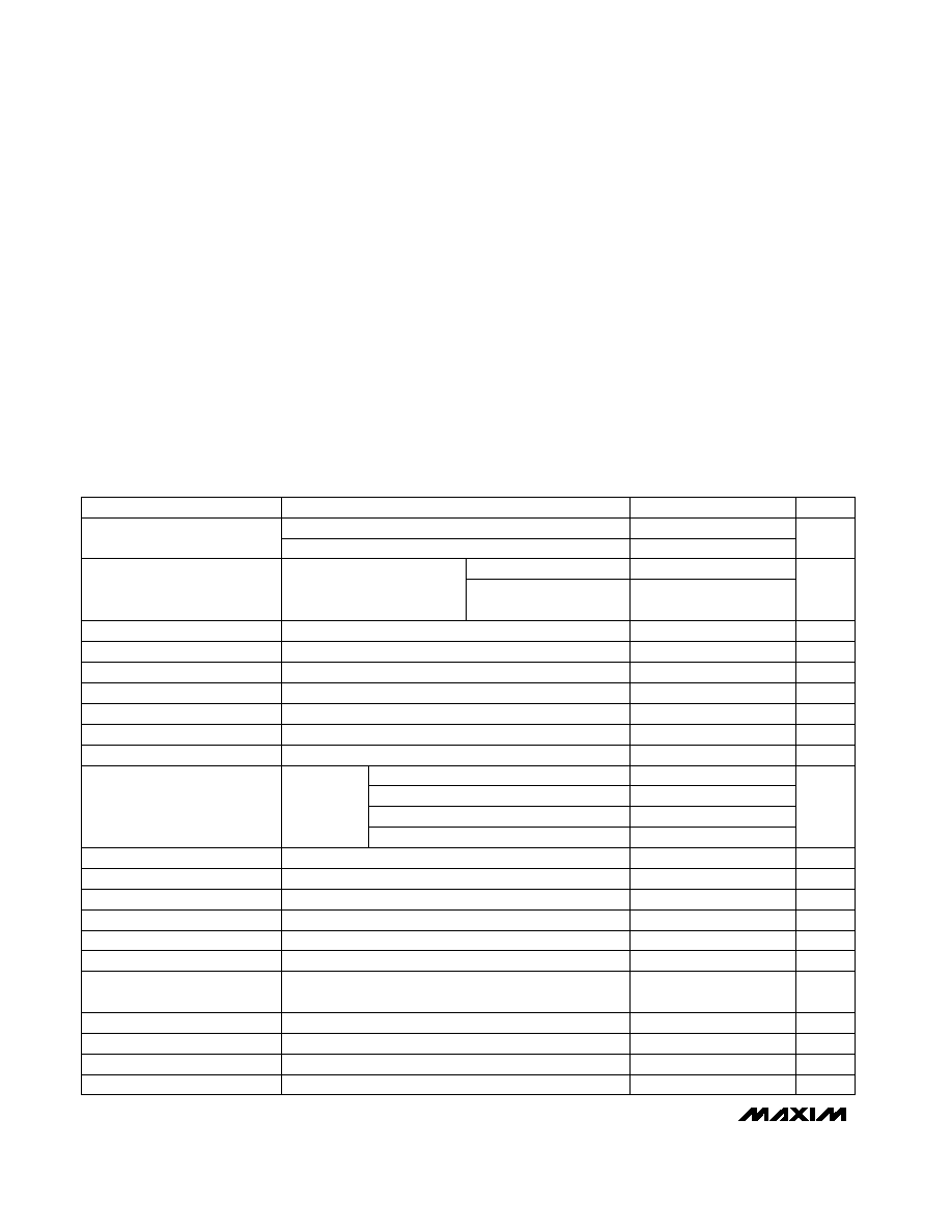
ABSOLUTE MAXIMUM RATINGS
Stresses beyond those listed under "Absolute Maximum Ratings" may cause permanent damage to the device. These are stress ratings only, and functional
operation of the device at these or any other conditions beyond those indicated in the operational sections of the specifications is not implied. Exposure to
absolute maximum rating conditions for extended periods may affect device reliability.
V+ to GND ..............................................................-0.3V to +30V
V
CC
, V
DD
to GND .....................................................-0.3V to +6V
PGND to GND.....................................................................±0.3V
SHDN, PGOOD to GND ...........................................-0.3V to +6V
OVP, ILIM, FB, FBS, CC, REF, D0≠D4,
GNDS, TON to GND ..............................-0.3V to (V
CC
+ 0.3V)
SKIP to GND (Note 1).................................-0.3V to (V
CC
+ 0.3V)
DL to PGND................................................-0.3V to (V
DD
+ 0.3V)
BST to GND ............................................................-0.3V to +36V
DH to LX .....................................................-0.3V to (BST + 0.3V)
LX to BST..................................................................-6V to +0.3V
REF Short Circuit to GND ...........................................Continuous
Continuous Power Dissipation (T
A
= +70∞C)
24-Pin QSOP (derate 9.5mW/∞C above +70∞C)..........762mW
Operating Temperature Range ...........................-40∞C to +85∞C
Junction Temperature ......................................................+150∞C
Storage Temperature Range .............................-65∞C to +165∞C
Lead Temperature (soldering, 10sec) .............................+300∞C
V
BATT
= 4.5V to 28V, includes
load regulation error
SHDN = 0, measured at V+ = 28V, V
CC
= V
DD
= 0 or 5V
SHDN = 0
V
CC,
V
DD
SHDN = 0
Battery voltage, V+
Measured at V+
Measured at V
DD
, FB forced above the regulation point
Measured at V
CC
, FB forced above the regulation point
Rising edge of SHDN to full I
LIM
(Note 2)
V
BATT
= 24V,
FB = 2V
(Note 2)
FB (MAX1710 only) or FBS
FB-FBS or GNDS-GND = 0 to 25mV
V
CC
= 4.5V to 5.5V, V
BATT
= 4.5V to 28V
CONDITIONS
µA
<1
5
Shutdown Battery Supply
Current
µA
<1
5
Shutdown Supply Current (V
DD
)
µA
<1
5
Shutdown Supply Current (V
CC
)
µA
25
40
Quiescent Battery Supply Current
µA
<1
5
Quiescent Supply Current (V
DD
)
µA
600
950
Quiescent Supply Current (V
CC
)
ns
400
500
Minimum Off-Time
380
425
470
260
290
320
175
200
225
%
-1
1
DC Output Voltage Accuracy
TON = REF (400kHz)
4.5
5.5
V
2
28
Input Voltage Range
TON = GND (550kHz)
ns
140
160
180
On-Time
ms
1.7
Soft-Start Ramp Time
µA
-1
1
GNDS Input Bias Current
µA
-0.2
0.2
FB Input Bias Current
TON = open (300kHz)
mV
3
Remote Sense Voltage Error
mV
5
Line Regulation Error
UNIT
MIN
TYP
MAX
PARAMETER
Falling edge, hysteresis = 40mV
REF in regulation
I
REF
= 0 to 50µA
V
CC
= 4.5V to 5.5V, no external REF load
V
1.6
REF Fault Lockout Voltage
µA
10
REF Sink Current
V
0.01
Reference Load Regulation
V
1.98
2
2.02
Reference Voltage
TON = V
CC
(200kHz)
Note 1:
SKIP may be forced below -0.3V, temporarily exceeding the absolute maximum rating, for the purpose of debugging proto-
type breadboards using the no-fault test mode. Limit the current drawn to -5mA maximum.
ELECTRICAL CHARACTERISTICS
(Circuit of Figure 1, V
BATT
= 15V, V
CC
= V
DD
= 5V, SKIP = GND,
T
A
=
0∞C to +85∞C
, unless otherwise noted.)
k
130
180
240
FB Input Resistance (MAX1711)
DAC codes from 1.3V to 2V
-1.2
1.2
I
LOAD
= 0 to 7A
mV
9
Load Regulation Error
DAC codes from 0.925V
to 1.275V

With respect to unloaded output voltage
MAX1710/MAX1711
High-Speed, Digitally Adjusted
Step-Down Controllers for Notebook CPUs
_______________________________________________________________________________________
3
ELECTRICAL CHARACTERISTICS (continued)
(Circuit of Figure 1, V
BATT
= 15V, V
CC
= V
DD
= 5V, SKIP = GND,
T
A
=
0∞C to +85∞C
, unless otherwise noted.)
CONDITIONS
UNIT
MIN
TYP
MAX
PARAMETER
LX to PGND
LX to PGND, ILIM tied to V
CC
From SHDN signal going high
mV
40
50
60
Current-Limit Threshold
(Positive Direction, Adjustable)
mV
90
100
110
Current-Limit Threshold
(Positive Direction, Fixed)
ms
10
30
Output Undervoltage Protection
Time
%
65
70
75
Output Undervoltage Protection
Threshold
LX to PGND, T
A
= +25∞C
mV
-150
-120
-80
Current-Limit Threshold
(Negative Direction)
R
LIM
= 100k
R
LIM
= 400k
170
200
230
Rising edge, hysteresis = 20mV,
PWM disabled below this level
V
4.1
4.4
V
CC
Undervoltage Lockout
Threshold
BST-LX forced to 5V
5
DH Gate-Driver On-Resistance
DL, high state
5
DL Gate-Driver On-Resistance
(Pull-Up)
DL, low state
0.5
1.7
DL Gate-Driver On-Resistance
(Pull-Down)
DH forced to 2.5V, BST-LX forced to 5V
A
1
DH Gate-Driver Source/Sink
Current
DL forced to 2.5V
A
3
DL Gate-Driver Sink Current
DL forced to 2.5V
A
1
DL Gate-Driver Source Current
FB forced 2% above trip threshold
µs
1.5
Overvoltage Fault Propagation
Delay
%
10.5
12.5
14.5
Overvoltage Trip Threshold
FB forced 2% below PGOOD trip threshold, falling edge
µs
1.5
PGOOD Propagation Delay
LX to PGND
mV
3
Current-Limit Threshold
(Zero Crossing)
I
SINK
= 1mA
V
0.4
PGOOD Output Low Voltage
High state, forced to 5.5V
µA
1
PGOOD Leakage Current
Hysteresis = 10∞C
∞C
150
Thermal Shutdown Threshold
V
2.21
2.25
2.29
0.76
0.8
0.84
With respect to unloaded output voltage (MAX1710)
With respect to unloaded output voltage (MAX1710)
(MAX1711)
V
DL rising
ns
35
Dead Time
DH rising
26
mA
SKIP Input Current Logic
Threshold
To enable no-fault mode, T
A
= +25∞C
-1.5
-0.1
%
PGOOD Trip Threshold
Measured at FB with respect to unloaded output voltage,
falling edge, hysteresis = 1%
-8
-5
-3
V
Logic Input High Voltage
D0≠D4, SHDN, SKIP, OVP
2.4
V
Logic Input Low Voltage
D0≠D4, SHDN, SKIP, OVP
0.8
µA
Logic Input Current
SHDN, SKIP, OVP
-1
1
µA
Logic Input Pull-Up Current
D0≠D4, each forced to GND
3
5
10
(MAX1711)

MAX1710/MAX1711
High-Speed, Digitally Adjusted
Step-Down Controllers for Notebook CPUs
4
_______________________________________________________________________________________
%
10
15
V
BATT
= 4.5V to 28V, for all
D/A codes, includes load
regulation error
V
CC,
V
DD
Battery voltage, V+
Measured at V
CC
, FB forced above the regulation point
Overvoltage Trip Threshold
(Note 2)
V
BATT
= 24V,
FB = 2V
(Note 2)
With respect to unloaded output voltage (MAX1710)
%
CONDITIONS
65
75
Output Undervoltage
Protection Threshold
µA
950
Quiescent Supply Current (V
CC
)
ns
500
Minimum Off-Time
380
470
260
320
175
225
%
-1.5
1.5
DC Output Voltage Accuracy
TON = REF (400kHz)
4.5
5.5
V
2
28
Input Voltage Range
TON = GND (550kHz)
ns
140
180
On-Time
TON = open (300kHz)
UNIT
MIN
TYP
MAX
PARAMETER
V
CC
= 4.5V to 5.5V, no external REF load
V
1.98
2.02
Reference Voltage
TON = V
CC
(200kHz)
LX to PGND, ILIM tied to V
CC
mV
85
115
Current-Limit Threshold
(Positive Direction, Fixed)
LX to PGND
mV
35
65
Current-Limit Threshold
(Positive Direction, Adjustable)
R
LIM
= 100k
R
LIM
= 400k
160
240
Rising edge, hysteresis = 20mV, PWM disabled below
this level
4.1
4.4
V
CC
Undervoltage Lockout
Threshold
V
D0≠D4, SHDN, SKIP, OVP
V
2.4
Logic Input High Voltage
D0≠D4, SHDN, SKIP, OVP
V
0.8
Logic Input Low Voltage
SHDN, SKIP, OVP
µA
-1
1
Logic Input Current
D0≠D4, each forced to GND
µA
3
10
Logic Input Pull-Up Current
ELECTRICAL CHARACTERISTICS
(Circuit of Figure 1, V
BATT
=15V, V
CC
= V
DD
= 5V, SKIP = GND,
T
A
= -40∞C to +85∞C,
unless otherwise noted.) (Note 3)
V
2.20
2.30
0.75
0.85
V
ELECTRICAL CHARACTERISTICS (continued)
(Circuit of Figure 1, V
BATT
= 15V, V
CC
= V
DD
= 5V, SKIP = GND,
T
A
=
0∞C to +85∞C
, unless otherwise noted.)
CONDITIONS
TON logic input high level
V
V
CC
- 0.4
TON V
CC
Level
TON logic input upper-mid-range level
V
3.15
3.85
TON Float Voltage
TON logic input lower-mid-range level
V
1.65
2.35
TON Reference Level
TON logic input low level
V
0.5
TON GND Level
TON only, forced to GND or V
CC
µA
-3
3
TON Logic Input Current
UNIT
MIN
TYP
MAX
PARAMETER
With respect to unloaded output voltage (MAX1710)
(MAX1711)
(MAX1711)
%
-1.7
1.7
DAC codes from 1.32V to 2V
DAC codes from 0.925V to
1.275V

MAX1710/MAX1711
High-Speed, Digitally Adjusted
Step-Down Controllers for Notebook CPUs
_______________________________________________________________________________________
5
40
60
50
80
70
90
100
0.01
0.1
1
10
EFFICIENCY vs. LOAD CURRENT
(V
O
= 2.0V, f = 300kHz)
MAX1710-01
LOAD CURRENT (A)
EFFICIENCY (%)
V
IN
= 4.5V
V
IN
= 7V
V
IN
= 15V
V
IN
= 24V
40
60
50
80
70
90
100
0.01
0.1
1
10
EFFICIENCY vs. LOAD CURRENT
(V
O
= 1.6V, f = 300kHz)
MAX1710-02
LOAD CURRENT (A)
EFFICIENCY (%)
V
IN
= 4.5V
V
IN
= 24V
V
IN
= 7V
V
IN
= 15V
40
60
50
80
70
90
100
0.01
0.1
1
10
EFFICIENCY vs. LOAD CURRENT
(V
O
= 1.3V, f = 300kHz)
MAX1710-03
LOAD CURRENT (A)
EFFICIENCY (%)
V
IN
= 4.5V
V
IN
= 24V
V
IN
= 15V
V
IN
= 7V
40
60
50
80
70
90
100
0.01
0.1
1
10
EFFICIENCY vs. LOAD CURRENT
(V
O
= 1.6V, f = 550kHz)
MAX1710-04
LOAD CURRENT (A)
EFFICIENCY (%)
V
IN
= 4.5V
V
IN
= 15V
V
IN
= 7V
V
IN
= 24V
0
100
50
200
150
300
250
350
0.01
0.1
1
10
FREQUENCY vs. LOAD CURRENT
(V
O
= 1.6V)
MAX1710-05
LOAD CURRENT (A)
FREQUENCY (kHz)
V
IN
= 15V, PWM MODE
V
IN
= 4.5V, SKIP MODE
V
IN
= 15V, SKIP MODE
TON = OPEN
300
306
304
302
308
310
312
314
316
318
320
0
10
5
15
20
25
30
FREQUENCY vs. INPUT VOLTAGE
(I
O
= 7A)
MAX1710-06
INPUT VOLTAGE (V)
FREQUENCY (kHz)
V
O
= 2.0V
V
O
= 1.6V
TON = OPEN
Note 2:
On-Time and Off-Time specifications are measured from 50% point to 50% point at the DH pin with LX forced to 0V, BST
forced to 5V, and a 250pF capacitor connected from DH to LX. Actual in-circuit times may differ due to MOSFET switching
speeds.
Note 3:
Specifications from -40∞C to 0∞C are guaranteed but not production tested.
__________________________________________Typical Operating Characteristics
(7A CPU supply circuit of Figure 1, T
A
= +25∞C, unless otherwise noted.)
CONDITIONS
Measured at FB with respect to unloaded output voltage,
falling edge, hysteresis = 1%
%
-8.5
-2.5
PGOOD Trip Threshold
I
SINK
= 1mA
V
0.4
PGOOD Output Low Voltage
High state, forced to 5.5V
µA
1
PGOOD Leakage Current
UNIT
MIN
TYP
MAX
PARAMETER
ELECTRICAL CHARACTERISTICS (continued)
(Circuit of Figure 1, V
BATT
=15V, V
CC
= V
DD
= 5V, SKIP = GND,
T
A
= -40∞C to +85∞C,
unless otherwise noted.) (Note 3)