 | –≠–ª–µ–∫—Ç—Ä–æ–Ω–Ω—ã–π –∫–æ–º–ø–æ–Ω–µ–Ω—Ç: MAX1739 | –°–∫–∞—á–∞—Ç—å:  PDF PDF  ZIP ZIP |

General Description
The MAX1739/MAX1839 fully integrated controllers are
optimized to drive cold-cathode fluorescent lamps
(CCFLs) using the industry-proven Royer oscillator
inverter architecture. The Royer architecture provides
near sinusoidal drive waveforms over the entire input
range to maximize the life of CCFLs. The MAX1739/
MAX1839 optimize this architecture to work over a wide
input voltage range, achieve high efficiency, and maxi-
mize the dimming range.
The MAX1739/MAX1839 monitor and limit the trans-
former center-tap voltage when required. This ensures
minimal voltage stress on the transformer, which
increases the operating life of the transformer and
eases its design requirements. These controllers also
provide protection against many other fault conditions,
including lamp-out and buck short faults.
These controllers achieve 50:1 dimming range by
simultaneously adjusting lamp current and "chopping"
the CCFL on and off using a digitally adjusted pulse-
width modulated (DPWM) method. CCFL brightness is
controlled by an analog voltage or is set with an
SMBus
TM
-compatible two-wire interface (MAX1739).
The MAX1739/MAX1839 drive an external high-side
N-channel power MOSFET and two low-side N-channel
power MOSFETs, all synchronized to the Royer oscilla-
tor. An internal 5.3V linear regulator powers the MOS-
FET drivers and most of the internal circuitry. The
MAX1739/MAX1839 are available in space-saving
20-pin QSOP packages and operate over the -40∞C to
+85∞C temperature range.
________________________Applications
Notebook/Laptop Computers
Car Navigation Displays
LCD Monitors
Point-of-Sale Terminals
Portable Display Electronics
Features
o Fast Response to Input Change
o Wide Input Voltage Range (4.6V to 28V)
o High Power-to-Light Efficiency
o Minimizes Transformer Voltage Stress
o Lamp-Out Protection with 2s Timeout
o Buck Switch Short and Other Single-Point Fault
Protection
o Integrated Royer MOSFET Drivers Reduce
Transformer Pin Count
o Buck Operation Synchronized to Royer Oscillator
o Synchronizable DPWM Frequency
o Pin-Selectable Brightness Control Interface
o SMBus Serial Interface (MAX1739)
o Analog Interface (MAX1739/MAX1839)
MAX1739/MAX1839
Wide Brightness Range
CCFL Backlight Controllers
________________________________________________________________ Maxim Integrated Products
1
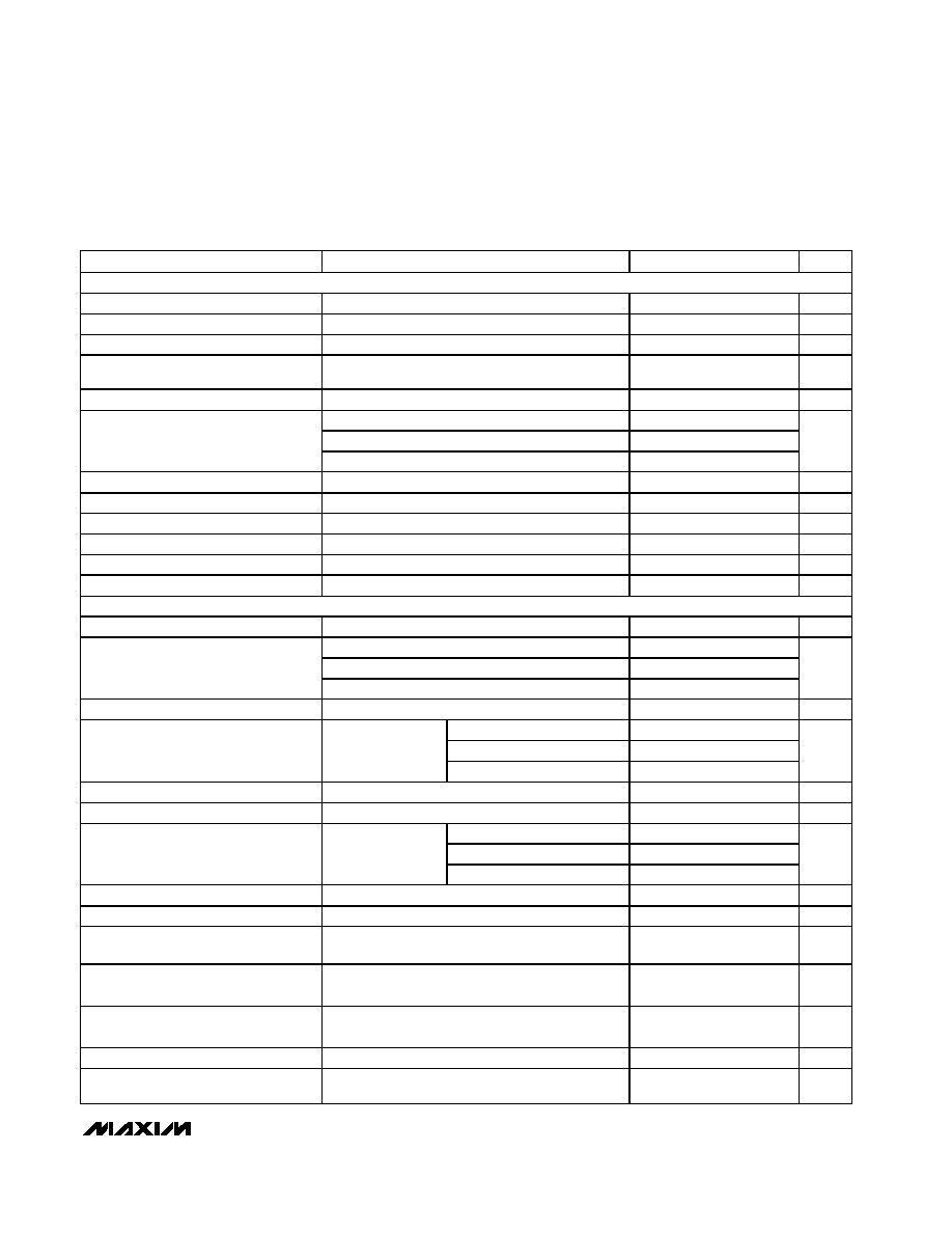
20
19
18
17
16
15
14
13
1
2
3
4
5
6
7
8
BATT
DH
LX
BST
CCV
CCI
MINDAC
REF
TOP VIEW
VL
GND
CS
DL1
MODE
CTL/SCL
CRF/SDA
SH/SUS
12
11
9
10
DL2
SYNC
CTFB
CSAV
MAX1739
QSOP
Pin Configuration
19-1755; Rev 1; 3/01
For price, delivery, and to place orders, please contact Maxim Distribution at 1-888-629-4642,
or visit Maxim's website at www.maxim-ic.com.
Patent pending
SMBus is a trademark of Intel Corp.
PART
TEMP. RANGE
PIN-PACKAGE
MAX1739EEP
-40
∞C to +85∞C
20 QSOP
MAX1839EEP
-40
∞C to +85∞C
20 QSOP
Ordering Information
Pin Configurations continued at end of data sheet.

MAX1739/MAX1839
Wide Brightness Range
CCFL Backlight Controllers
2
_______________________________________________________________________________________
ABSOLUTE MAXIMUM RATINGS
ELECTRICAL CHARACTERISTICS
(V+ = 8.2V, V
SH
/SUS = V
SH
= 5.5V, MINDAC = GND, T
A
= 0∞C to +85∞C, unless otherwise noted. Typical values are at T
A
= +25∞C.)
Stresses beyond those listed under "Absolute Maximum Ratings" may cause permanent damage to the device. These are stress ratings only, and functional
operation of the device at these or any other conditions beyond those indicated in the operational sections of the specifications is not implied. Exposure to
absolute maximum rating conditions for extended periods may affect device reliability.
V
BATT
to GND ...........................................................-0.3V to 30V
V
BST
, V
SYNC
to GND.................................................-0.3V to 34V
V
BST
to V
LX
.................................................................-0.3V to 6V
V
DH
to V
LX
.................................................-0.3V to (V
BST
+ 0.3V)
V
LX
to GND...................................................-6V to (V
BST
+ 0.3V)
VL to GND...................................................................-0.3V to 6V
V
CCV
, V
CCI
, V
REF
, V
DL1
, V
DL2
to GND .........-0.3V to (VL + 0.3V)
V
MINDAC
, V
CTFB
, V
CSAV
to GND ................................-0.3V to 6V
V
CS
to GND...................................................-0.6V to (VL + 0.3V)
V
MODE
to GND.............................................................-6V to 12V
V
CRF/SDA
, V
CRF
, V
CTL/SCL
, V
CTL
, V
SH/SUS
,
V
SH
to GND ............................................................-0.3V to 6V
Continuous Power Dissipation (T
A
= +70∞C)
20-Pin QSOP (derate 9.1mW/∞C above +70∞C)...........727mW
Operating Temperature .......................................-40∞C to +85∞C
Storage Temperature.........................................-65∞C to +150∞C
Lead Temperature (soldering, 10s) .................................+300∞C
PARAMETER
CONDITIONS
MIN
TYP
MAX
UNITS
SUPPLY AND REFERENCE
V
L
= V
BATT
4.6
5.5
V
BATT
Input Voltage Range
V
L
= open
6
28
V
V
BATT
= 28V
3.2
6
V
BATT
Quiescent Current, Operation
with Full Duty Cycle on DH
DH = DL1 = DL2 = open
V
BATT
= V
L
= 5V
3.2
6
mA
V
BATT
Quiescent Current, Shutdown
SH/SUS = SH = GND
6
20
µA
VL Output Voltage, Normal Operation
6V < V
BATT
< 28V, 0 < I
LOAD
< 15mA
5.0
5.35
5.5
V
VL Output Voltage, Shutdown
SH/SUS = SH = GND, no load
3.5
4.5
5.5
V
VL rising (leaving lockout)
4.6
VL Undervoltage Lockout Threshold
VL falling (entering lockout)
4.0
V
VL Undervoltage Lockout Hysteresis
300
mV
REF Output Voltage, Normal
Operation
4.5V < VL < 5.5V, I
REF
= 40
µA
1.96
2.00
2.04
V
V
L
POR Threshold
0.9
2.7
V
SWITCHING REGULATOR
DH Driver On-Resistance
18
DL1, DL2 Driver On-Resistance
18
Minimum DH Switching Frequency
1/t
DH
, SYNC = CS or GND, not synchronized
49
56
64
kHz
DH Minimum Off-Time
250
375
500
ns
DH Maximum Duty Cycle
98
%
SYNC Synchronization Range
Detect falling edges on SYNC
64
200
kHz
SYNC Input Current
0 < V
SYNC
< 30V
-2
2
µA
SYNC Input Threshold
SYNC falling, referred to CS
400
500
600
mV
SYNC Input Hysteresis
Referred to the SYNC input threshold
50
100
150
mV
SYNC Threshold Crossing to DL1,
DL2 Toggle Delay
V
SYNC
= 0 to 5V, C
DL_1
and
C
DL_2
< 100pF,
50% point on SYNC to 50% point on DL1 or DL2
120
ns
CS Overcurrent Threshold
408
450
492
mV
MAX1739/MAX1839
Wide Brightness Range
CCFL Backlight Controllers
_______________________________________________________________________________________
3
ELECTRICAL CHARACTERISTICS (continued)
(V+ = 8.2V, V
SH
/SUS = V
SH
= 5.5V, MINDAC = GND, T
A
= 0∞C to +85∞C, unless otherwise noted. Typical values are at T
A
= +25∞C.)
PARAMETER
CONDITIONS
MIN
TYP
MAX
UNITS
DAC AND ERROR AMPLIFIER
DAC Resolution
Guaranteed monotonic
5
Bits
MINDAC Input Voltage Range
0
2
V
MINDAC Input Bias Current
0 < V
MINDAC
< 2V
-1
1
µA
MINDAC Digital PWM Disable
Threshold
MINDAC = VL
2.4
2.9
4
V
CSAV Input Voltage Range
0
0.8
V
V
MINDAC
= 0, DAC code = 11111 binary
188
194
200
V
MINDAC
= 0, DAC code = 00001 binary
2
6.25
16
CSAV Regulation Point
V
MINDAC
= 1V, DAC code = 00000 binary
93
100
110
mV
CSAV Input Bias Current
-1
1
µA
CSAV to CCI Transconductance
1V < V
CCI
< 2.7V
100
µmho
CTFB Input Voltage Range
0
2
V
CTFB Input Bias Current
-1
1
µA
CTFB Regulation Point
570
600
630
mV
CTFB to CCV Transconductance
1V < V
CCV
< 2.7V
30
40
50
µmho
TIMERS AND FAULT DETECTION
Chopping Oscillator Frequency
No AC signal on MODE, not synchronized
24
28
32
kHz
No AC signal on MODE
205
220
235
32kHz AC signal on MODE
250
Digital PWM Chop-Mode Frequency
100kHz AC signal on MODE
781
Hz
MODE to DPWM Sync Ratio
F
MODE
/ F
DPWM
128
No AC signal on MODE
2.06
2.33
2.73
32kHz AC signal on MODE
2.05
Lamp-Out Detection Timeout Timer
(Center-Tap Voltage Stuck at
Maximum) (Note 1)
V
CSAV
< CSAV
lamp-out
threshold
100kHz AC signal on MODE
0.66
s
CSAV Lamp-Out Threshold
50
75
100
mV
Fault-Detection Threshold on CCV
(Note 2)
0.4
1
V
No AC signal on MODE
332
291
259
32kHz AC signal on MODE
256
Shorted Buck-Switch Detection
Timeout Timer (UL1950 Protection)
(Note 3)
V
CCV
< fault-
detection
threshold on CCV
100kHz AC signal on MODE
82
ms
Lamp Turn-On Delay
After
SH/SUS or SH forces device on or SH rises
4
ms
MODE Operating Voltage Range
-5.5
11
V
MODE = GND Threshold
(min Brightness = 0)
To sync DPWM oscillator, not in shutdown
(Note 4)
0.6
V
MODE = REF Threshold
(max Brightness = 0)
To sync DPWM oscillator, not in shutdown
(Note 4)
1.4
2.6
V
MODE = VL Threshold
(MAX1739 SMB Interface Mode)
To sync DPWM oscillator, not in shutdown
(Note 4)
VL - 0.6
V
MODE AC Signal Amplitude
Peak to peak (Note 5)
2
V
MODE AC Signal Synchronization
Range
Chopping oscillator synchronized to MODE AC
signal
32
100
kHz
MAX1739/MAX1839
Wide Brightness Range
CCFL Backlight Controllers
4
_______________________________________________________________________________________
ELECTRICAL CHARACTERISTICS (continued)
(V+ = 8.2V, V
SH
/SUS = V
SH
= 5.5V, MINDAC = GND, T
A
= 0∞C to +85∞C, unless otherwise noted. Typical values are at T
A
= +25∞C.)
PARAMETER
CONDITIONS
MIN
TYP
MAX
UNIT
ANALOG INTERFACE BRIGHTNESS CONTROL (MODE connected to REF or GND )
CRF/SDA, CRF Input Range
2.7
5.5
V
V
CRF/SDA
= V
CRF
= 5.5V
20
µA
CRF/SDA, CRF Input Current
V
CRF/SDA
= V
CRF
= 5.5V, SH/SUS = SH = 0
-1
1
µA
CTL/SCL, Input Range
MAX1739
0
CRF/
SDA
V
CTL Input Range
MAX1839
0
CRF
V
CTL/SCL, CTL Input Current
MODE = REF or GND
-1
1
µA
ADC Resolution
Guaranteed monotonic
5
Bits
ADC Hysteresis
1
LSB
SH Input Low Voltage
0.8
V
SH Input High Voltage
2.1
V
SH/SUS Input Hysteresis when
Transitioning In and Out of Shutdown
150
mV
SH Input Bias Current
-1
1
µA
SYSTEM MANAGEMENT BUS BRIGHTNESS CONTROL (MAX1739, MODE connected to V
L
, see Figures 12 and 13)
CRF/SDA, CTL/SCL, SH/SUS Input
0.8
V
CRF/SDA, CTL/SCL, SH/SUS Input
2.1
V
CRFSDA, CTLSCL Input Hysteresis
300
mV
CRF/SDA, CTL/SCL, SH/SUS Input
-1
1
µA
CRF/SDA Output Low Sink Current
V
CRF/SDA
= 0.4V
4
mA
CTL/SCL Serial Clock High Period
t
HIGH
4
µs
CTL/SCL Serial Clock Low Period
t
LOW
4.7
µs
Start Condition Setup Time
t
SU:STA
4.7
µs
Start Condition Hold Time
t
HD:STA
4
µs
C RF/S D A V al id to C TL/S C L Ri si ng E d g e
S etup Ti m e, S l ave C l ocki ng i n D ata
t
SU:DAT
250
ns
CTL/SCL Falling Edge to CRF/SDA
Transition
t
HD:DAT
0
ns
CTL/SCL Falling Edge to CRF/SDA
Valid, Reading Out Data
t
DV
1
µs

MAX1739/MAX1839
Wide Brightness Range
CCFL Backlight Controllers
_______________________________________________________________________________________
5
ELECTRICAL CHARACTERISTICS
(V+ = 8.2V, V
SH
/SUS = V
SH
= 5.5V, MINDAC = GND, T
A
= -40∞C to +85∞C, unless otherwise noted.) (Note 6)
PARAMETER
CONDITIONS
MIN
TYP
MAX
UNITS
SUPPLY AND REFERENCE
VL = V
BATT
4.6
5.5
V
BATT
Input Voltage Range
VL = open
6
28
V
V
BATT
Quiescent Current, Shutdown
SH/SUS = SH = GND
20
µA
VL Output Voltage, Normal Operation
6V < V
BATT
< 28V,
0 < I
LOAD
< 15mA
5.0
5.6
V
VL rising (leaving lockout)
4.6
VL Undervoltage Lockout Threshold
VL falling (entering lockout)
4.0
V
REF Output Voltage, Normal
Operation
4.5V < VL < 5.5V, I
REF
= 40µA
1.95
2.05
V
VL POR Threshold
0.9
2.7
V
SWITCHING REGULATOR
DH Driver On-Resistance
18
DL1, DL2 Driver On-Resistance
18
SYNC Synchronization Range
Detect falling edges on SYNC
64
200
kHz
CS Overcurrent Threshold
408
492
mV
DAC AND ERROR AMPLIFIER
CSAV Regulation Point
V
MINDAC
= 0, DAC code = 11111 binary
186
202
mV
CTFB Regulation Point
560
640
mV
CTFB to CCV Transconductance
1V < V
CCV
< 2.7V
30
50
µmho
ANALOG INTERFACE BRIGHTNESS CONTROL (MODE connected to REF or MODE connected to GND)
SH Input Low Voltage
0.8
V
SH Input High Voltage
2.1
V
SYSTEM MANAGEMENT BUS BRIGHTNESS CONTROL (MODE connected to VL)
CRF/SDA, CTL/SCL, SH/SUS Input
Low Voltage
0.8
V
CRF/SDA, CTL/SCL, SH/SUS Input
High Voltage
2.1
V
CRF/SDA Output Low Sink Current
V
CRF/SDA
= 0.4V
4
mA
Note 1: Corresponds to 512 DPWM cycles or 65536 MODE
cycles.
Note 2: When the buck switch is shorted, V
CTFB
goes high
causing V
CCV
to go below the fault detection threshold.
Note 3: Corresponds to 64 DPWM cycles or 8192 MODE cycles.
Note 4: The MODE pin thresholds are only valid while the part is
operating. In shutdown, V
REF
= 0 and the part only
differentiates between SMB mode and ADC mode. In
shutdown with ADC mode selected, the CRF/SDA and
CTL/SCL pins are at high impedance and will not cause
extra supply current when their voltages are not at
GND or VL.
V
AMPLITUDE
> 2V
MODE
500pF
10k
Note 5: The amplitude is measured with the following circuit:
Note 6: Specifications from -40∞C to +85∞C are guaranteed by
design, not production tested.