 | ÐлекÑÑоннÑй компоненÑ: MAX1792 | СкаÑаÑÑ:  PDF PDF  ZIP ZIP |
Äîêóìåíòàöèÿ è îïèñàíèÿ www.docs.chipfind.ru
For price, delivery, and to place orders, please contact Maxim Distribution at 1-888-629-4642,
or visit Maxim's website at www.maxim-ic.com.
General Description
The MAX1792 low-dropout linear regulator operates
from a +2.5V to +5.5V supply and delivers a guaran-
teed 500mA load current with low 130mV dropout. The
high-accuracy (±1%) output voltage is preset at an
internally trimmed voltage (see Selector Guide) or can
be adjusted from 1.25V to 5.0V with an external resis-
tive divider.
An internal PMOS pass transistor allows the low 80µA
supply current to remain independent of load, making
this device ideal for portable battery-operated equip-
ment such as personal digital assistants (PDAs), cellu-
lar phones, cordless phones, base stations, and
notebook computers.
Other features include an active-low open-drain reset
output with a 4ms timeout period that indicates when
the output is out of regulation, a 0.1µA shutdown mode,
short-circuit protection, and thermal shutdown protec-
tion. The device is available in a miniature 1.3W, 8-pin
power-µMAX package with a metal pad on the under-
side of the package.
________________________Applications
Notebook Computers
Cellular and Cordless Telephones
Personal Digital Assistants (PDAs)
Palmtop Computers
Base Stations
USB Hubs
Docking Stations
Features
o Guaranteed 500mA Output Current
o Low 130mV Dropout at 500mA
o Up to ±1% Output Voltage Accuracy
Preset at 1.5V, 1.8V, 2.5V, 3.3V, or 5.0V
Adjustable from 1.25V to 5.0V
o Reset Output with 4ms Timeout Period
o Low 80µA Ground Current
o 0.1µA Shutdown Current
o Thermal Overload Protection
o Output Current Limit
o Tiny 1.3W Power-µMAX Package
MAX1792
500mA Low-Dropout
Linear Regulator in µMAX
________________________________________________________________ Maxim Integrated Products
1
SET
GND
SHDN
1
2
8
7
OUT
OUT
IN
RST
IN
POWER-
µMAX
TOP VIEW
3
4
6
5
MAX1792
Pin Configuration
NC
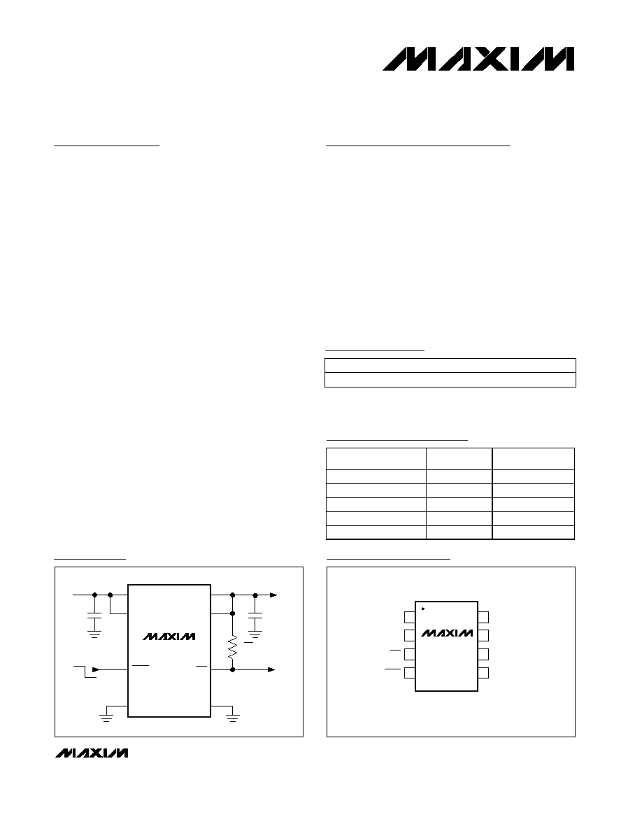
MAX1792
IN
IN
C
IN
1
µF
C
OUT
3.3
µF
R
RST
100k
V
IN
= +2.5V TO +5.5V
ON
OFF
SHDN
OUT
V
OUT
OUT
RST
GND
SET
TO
µC
Typical Operating Circuit
19-1699; Rev 0; 9/00
Ordering Information
Selector Guide
PART AND
SUFFIX
V
OUT
µMAX
TOP MARK
MAX1792EUA15
1.5V or Adj.
AAAE
MAX1792EUA18
1.8V or Adj.
AAAA
MAX1792EUA25
2.5V or Adj.
AAAB
MAX1792EUA33
3.3V or Adj.
AAAC
MAX1792EUA50
5.0V or Adj.
AAAD
PART*
TEMP RANGE
PIN-PACKAGE
MAX1792EUA_ _
-40
°C to +85°C
8 Power-
µMAX
*Insert the desired two-digit suffix (see Selector Guide) into the
blanks to complete the part number.
Contact factory for other preset output voltages.
MAX1792
500mA Low-Dropout
Linear Regulator in µMAX
2
_______________________________________________________________________________________
ABSOLUTE MAXIMUM RATINGS
ELECTRICAL CHARACTERISTICS
(V
IN
= V
OUT(NOM)
+ 500mV, or V
IN
= +2.5V (whichever is greater), SHDN = IN, T
A
= 0°C to +85°C, unless otherwise noted. Typical
values are at T
A
= +25°C.)
Stresses beyond those listed under "Absolute Maximum Ratings" may cause permanent damage to the device. These are stress ratings only, and functional
operation of the device at these or any other conditions beyond those indicated in the operational sections of the specifications is not implied. Exposure to
absolute maximum rating conditions for extended periods may affect device reliability.
IN, SHDN, RST, SET to GND ....................................-0.3V to +6V
OUT to GND ................................................-0.3V to (V
IN
+ 0.3V)
Output Short-Circuit Duration ........................................Indefinite
Continuous Power Dissipation (T
A
= +70°C)
8-Pin Power-µMAX (derate 17mW/°C above +70°C) .......1.3W
Operating Temperature Range ...........................-40°C to +85°C
Junction Temperature ......................................................+150°C
Storage Temperature Range .............................-65°C to +150°C
Lead Temperature (soldering, 10s) .................................+300°C
PARAMETER
SYMBOL
CONDITIONS
MIN
TYP
MAX
UNITS
Input Voltage
V
IN
2.5
5.5
V
Input Undervoltage Lockout
V
UVLO
Rising, 75mV hysteresis
2.0
2.15
2.3
V
Preset V
OUT
2.5V
-1
+1
I
OUT
= 100mA,
T
A
= +85
°C
Preset V
OUT
< 2.5V
-1.5
+1.5
%
I
OUT
= 100mA, T
A
= 0
°C to +85°C
-2
+2
Output Voltage Accuracy
(Preset Mode)
V
OUT
I
OUT
= 1mA to 500mA, V
IN
> V
OUT
+ 0.5V,
T
A
= 0
°C to +85°C
-3
+3
%
Adjustable Output Voltage
Range
1.25
5
V
T
A
= +85
°C
1.229
1.250
1.271
SET Voltage Threshold
(Adjustable Mode)
V
SET
V
IN
= +2.7V,
V
OUT
set to 2.0V,
I
OUT
= 100mA
T
A
= 0
°C to +85°C
1.219
1.281
V
Maximum Output Current
I
OUT
V
IN
2.7V
500
mA
RMS
Short-Circuit Current Limit
I
LIM
V
OUT
= 0, V
IN
2.7V
0.55
0.8
1.8
A
In-Regulation Current Limit
V
OUT
> 96% of nominal value, V
IN
2.7V
1.6
A
SET Dual ModeTM Threshold
50
100
150
mV
SET Input Bias Current
I
SET
V
SET
= 1.25V
-100
+100
nA
I
OUT
= 1mA
80
250
Ground-Pin Current
I
Q
I
OUT
= 500mA
110
µA
V
OUT
= 5.0V
120
225
V
OUT
= 3.3V
130
250
Dropout Voltage (Note 1)
V
IN
-
V
OUT
I
OUT
= 500mA
V
OUT
= 2.5V
210
360
mV
Line Regulation
V
LNR
V
IN
from (V
OUT
+ 100mV) to 5.5V,
I
LOAD
= 5mA
-0.15
0
+0.15
%/V
Load Regulation
V
LDR
I
OUT
= 1mA to 500mA
0.4
1.0
%
Output Voltage Noise
10Hz to 1MHz, C
OUT
= 3.3
µF (ESR < 0.1)
115
µV
RMS
SHUTDOWN
Shutdown Supply Current
I
OFF
SHDN = GND, V
IN
= 5.5V
0.1
15
µA
V
IH
2.5V < V
IN
< 5.5V
1.6
SHDN Input Threshold
V
IL
2.5V < V
IN
< 5.5V
0.6
V
SHDN Input Bias Current
SHDN = IN or GND
10
100
nA
Dual Mode is a trademark of Maxim Integrated Products.
MAX1792
500mA Low-Dropout
Linear Regulator in µMAX
_______________________________________________________________________________________
3
ELECTRICAL CHARACTERISTICS
(V
IN
= V
OUT(NOM)
+ 500mV, or V
IN
= +2.5V (whichever is greater), SHDN = IN, T
A
= -40°C to +85°C, unless otherwise noted.) (Note 2)
ELECTRICAL CHARACTERISTICS (continued)
(V
IN
= V
OUT(NOM)
+ 500mV, or V
IN
= +2.5V (whichever is greater), SHDN = IN, T
A
= 0°C to +85°C, unless otherwise noted. Typical
values are at T
A
= +25°C.)
PARAMETER
SYMBOL
CONDITIONS
MIN
TYP
MAX
UNITS
RESET OUTPUT
Reset Output Low Voltage
V
OL
RST sinking 1mA
0.01
0.1
V
Operating Voltage Range for
Valid Reset
RST sinking 100
µA
1.0
5.5
V
RST Output High Leakage
Current
V
RST
= +5.5V
100
nA
RST Threshold
Rising edge, referred to V
OUT(NOMINAL)
90
93
96
%
RST Release Delay
t
RP
Rising edge of OUT to rising edge of RST
1.5
4.5
8
ms
THERMAL PROTECTION
Ther m al S hutd ow n Tem p er atur e
T
SHDN
170
°C
Thermal Shutdown Hysteresis
T
SHDN
20
°C
PARAMETER
SYMBOL
CONDITIONS
MIN
MAX
UNITS
Input Voltage
V
IN
2.5
5.5
V
Input Undervoltage Lockout
V
UVLO
Rising or falling
2.0
2.3
V
I
OUT
= 100mA
-2
+2
Output Voltage Accuracy
(Preset Mode)
V
OUT
I
OUT
= 1mA to 500mA
-3
+3
%
Adjustable Output Voltage
Range
1.25
5
V
SET Voltage Threshold
(Adjustable Mode)
V
SET
I
OUT
= 100mA
1.212
1.288
V
Maximum Output Current
I
OUT
500
mA
RMS
Short-Circuit Current Limit
I
LIM
V
OUT
= 0
0.55
1.8
A
SET Dual Mode Threshold
50
150
mV
SET Input Bias Current
I
SET
V
SET
= 1.25V
-100
+100
nA
Ground-Pin Current
I
Q
I
OUT
= 1mA
250
µA
V
OUT
= 5.0V
225
V
OUT
= 3.3V
250
Dropout Voltage (Note 1)
V
IN
-
V
OUT
I
OUT
= 500mA
V
OUT
= 2.5V
360
mV
Line Regulation
V
LNR
V
IN
from (V
OUT
+ 100mV) to 5.5V,
I
LOAD
= 5mA
-0.15
+0.15
%/V
Load Regulation
V
LDR
I
OUT
= 1mA to 500mA
1.0
%
SHUTDOWN
Shutdown Supply Current
I
OFF
SHDN = GND, V
IN
= +5.5V
15
µA
V
IH
2.5V < V
IN
< 5.5V
1.6
SHDN Input
Threshold
V
IL
2.5V < V
IN
< 5.5V
0.6
V
SHDN Input Bias Current
I
SHDN
SHDN = IN or GND
100
nA
0
1.0
0.5
2.0
1.5
3.0
2.5
3.5
2.0
3.0
3.5
2.5
4.0
4.5
5.0
5.5
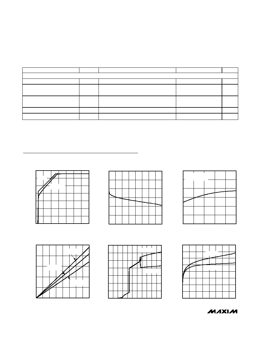
OUTPUT VOLTAGE
vs. INPUT VOLTAGE
MAX1792-01
INPUT VOLTAGE (V)
OUTPUT VOLTAGE (V)
I
OUT
= 0
I
OUT
= 500mA
3.27
3.28
3.29
3.30
3.31
3.32
3.33
0
200
100
300 400 500 600 700 800
OUTPUT VOLTAGE
vs. LOAD CURRENT
MAX1792-02
LOAD CURRENT (mA)
OUTPUT VOLTAGE (V)
3.27
3.29
3.28
3.31
3.30
3.32
3.33
-40
10
-15
35
60
85
OUTPUT VOLTAGE
vs. TEMPERATURE
MAX1792-03
TEMPERATURE (°C)
OUTPUT VOLTAGE (V)
V
IN
= V
OUT
+ 500mV
I
OUT
= 0
0
50
150
100
200
250
0
200 300
100
400 500 600 700 800
DROPOUT VOLTAGE
vs. LOAD CURRENT
MAX1792-04
LOAD CURRENT (mA)
DROPOUT VOLTAGE (mV)
T
A
= +85
°C
T
A
= -40
°C
T
A
= +25
°C
0
40
20
80
60
120
100
140
0
1.0 1.5 2.0
0.5
2.5 3.0 3.5 4.0 4.5 5.0 5.5
GROUND-PIN CURRENT
vs. INPUT VOLTAGE
MAX1792-05
INPUT VOLTAGE (V)
GROUND-PIN CURRENT (
µ
A)
I
OUT
= 500mA
I
OUT
= 0
60
80
70
100
90
110
120
130
140
0
200 300
100
400 500 600 700 800
GROUND-PIN CURRENT
vs. LOAD CURRENT
MAX1792-06
LOAD CURRENT (mA)
GROUND-PIN CURRENT (
µ
A)
V
IN
= 5.5V
V
IN
= 3.8V
Typical Operating Characteristics
(MAX1792EUA33, V
IN
= V
OUT
+ 500mV, SHDN = IN, C
IN
= 1µF, C
OUT
= 3.3µF, T
A
= +25°C, unless otherwise noted.)
MAX1792
500mA Low-Dropout
Linear Regulator in µMAX
4
_______________________________________________________________________________________
PARAMETER
SYMBOL
CONDITIONS
MIN
MAX
UNITS
RESET OUTPUT
Reset Output Low Voltage
V
OL
RST sinking 1mA
0.1
V
Operating Voltage Range for
Valid Reset
RST sinking 100
µA
1.0
5.5
V
RST Output High Leakage
Current
V
RST
= +5.5V
100
nA
RST Threshold
Rising edge, referred to V
OUT(NOMINAL)
90
96
%
RST Release Delay
t
RP
Rising edge of OUT to rising edge of RST
1.5
8
ms
ELECTRICAL CHARACTERISTICS (continued)
(V
IN
= V
OUT(NOM)
+ 500mV, or V
IN
= +2.5V (whichever is greater), SHDN = IN, T
A
= -40°C to +85°C, unless otherwise noted.) (Note 2)
Note 1: Dropout voltage is defined as V
IN
- V
OUT
, when V
OUT
is 100mV below the value of V
OUT
measured when V
IN
= V
OUT(NOM)
+ 0.5V. Since the minimum input voltage is 2.5V, this specification is only meaningful when V
OUT(NOM)
2.5V. For V
OUT(NOM)
between 2.5V and 3.5V, use the following equations: Typical Dropout = -93mV/V
V
OUT(NOM)
+ 445mV; Guaranteed Maximum
Dropout = -137mV/V
V
OUT(NOM)
+ 704mV. For V
OUT(NOM)
3.5V: Typical Dropout = 120mV; Guaranteed Maximum Dropout
= 225mV.
Note 2: Specifications to -40°C are guaranteed by design, not production tested.
MAX1792
500mA Low-Dropout
Linear Regulator in µMAX
_______________________________________________________________________________________
5
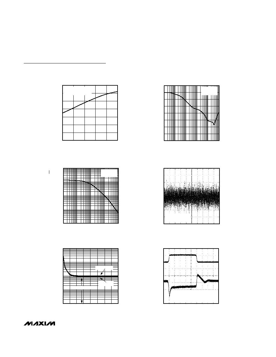
OUTPUT NOISE DC TO 1MHz
MAX1792-10
20ms/div
V
OUT
200
µV/div
V
OUT
= 3.3V
R
OUT
= 66
(50mA)
100
0.01
0
200
100
400
600
REGION OF STABLE C
OUT
ESR
vs. LOAD CURRENT
0.1
1
10
MAX1792-11
LOAD CURRENT (mA)
C
OUT
ESR (
)
300
500
700
800
STABLE REGION
C
OUT
= 3.3
µF
C
OUT
= 10
µF
LOAD-TRANSIENT RESPONSE
MAX1792-12
10
µs/div
I
OUT
500mA/div
V
OUT
20mV/div
V
IN
= V
OUT
+ 500mV
C
IN
= 10
µF
R
OUT
= 660
TO 6.6 (5mA TO 500mA)
60
70
65
80
75
90
85
95
-40
10
-15
35
60
85
GROUND-PIN CURRENT
vs. TEMPERATURE
MAX1792-07
TEMPERATURE (
°C)
GROUND-PIN CURRENT (
µ
A)
V
IN
= V
OUT
+ 500 mV
I
OUT
= 0
-80
0
0.01
0.1
1000
POWER-SUPPLY REJECTION RATIO
vs. FREQUENCY
-10
-30
-60
-70
MAX1792-08
FREQUENCY (kHz)
PSRR (dB)
1
10
-50
-40
-20
100
C
OUT
= 3.3
µF
I
OUT
= 50mA
0.1
1
10
100
1000
OUTPUT SPECTRAL NOISE DENSITY
vs. FREQUENCY
MAX1792-09
FREQUENCY (kHz)
OUTPUT SPECTRAL NOISE DENSITY (
µ
V/
Hz)
10
0.001
0.01
0.1
1
C
OUT
= 3.3
µF
I
OUT
= 50mA
Typical Operating Characteristics (continued)
(MAX1792EUA33, V
IN
= V
OUT
+ 500mV, SHDN = IN, C
IN
= 1µF, C
OUT
= 3.3µF, T
A
= +25°C, unless otherwise noted.)