 | –≠–ª–µ–∫—Ç—Ä–æ–Ω–Ω—ã–π –∫–æ–º–ø–æ–Ω–µ–Ω—Ç: MAX1838 | –°–∫–∞—á–∞—Ç—å:  PDF PDF  ZIP ZIP |

General Description
The MAX1838 is a dual, current-limited USB switch with
auxiliary input supply. Each switch meets all IEC speci-
fications for USB ports and is guaranteed to supply
500mA from either of two input supplies. A control pin
selects the power source from either the main or auxil-
iary supply.
The MAX1838 has multiple protection features, includ-
ing independent thermal-shutdown on each channel to
limit junction temperature in case of a prolonged short
or overload condition. The device has accurate internal
current-limit and reverse-current protection to safe-
guard the input supply against overload. When pow-
ered from the auxiliary supply, the current limit on each
channel is set independently with an external resistor.
An autoreset feature latches the switch off if the output
is shorted, thereby saving system power. When the
short is removed, the switch automatically turns back
on. Independent fault signals (FAULTA and FAULTB)
notify the microprocessor (µP) that the internal current
limit has been reached. A 20ms fault-blanking feature
prevents the MAX1838 from issuing false alarms to the
host during power-up or when hot-swapping into a
capacitive load.
The MAX1838 is available in a space-saving 16-pin
QSOP. For other USB current-limited switches, refer to
the MAX1693, MAX1694, MAX1812, and MAX1823.
Applications
Desktops
Notebook Computers
USB Ports
Docking Stations
Features
o Dual USB Switch with Auxiliary Input
o Autoreset from Fault Condition
o Guaranteed 500mA Load per Channel
o Programmable Current Limits on Auxiliary Inputs
o Reverse Current Protection
o Thermal Overload Protection
o Built-In 20ms Fault-Blanking
o 4V to 5.5V Range
o Independent FAULT Indicator Outputs
o UL Listing Pending
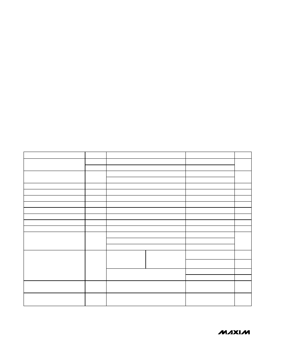
MAX1838
Dual USB Switch with Fault Blanking
and Autoreset
________________________________________________________________ Maxim Integrated Products
1
16
15
14
13
12
11
10
9
1
2
3
4
5
6
7
8
GND
FAULTA
ADJA
OUTA2
OUTA1
OUTB2
OUTB1
ADJB
FAULTB
TOP VIEW
MAX1838
QSOP
SEL
AUXA
AUXB
INA
INB
ON
GND
Pin Configuration
Ordering Information
19-2033; Rev 0; 4/01
PART
TEMP. RANGE
PIN-PACKAGE
MAX1838EEE
-40
∞C to +85∞C
16 QSOP
FAULTB
FAULTA
OUTB
OUTA
ADJB
ADJA
AUXA
AUXB
INA
INB
SEL
ON
GND
AUX
IN
OUTB
OUTA
10
µF
MAX1838
Typical Operating Circuit
For pricing, delivery, and ordering information, please contact Maxim/Dallas Direct! at
1-888-629-4642, or visit Maxim's website at www.maxim-ic.com.
MAX1838
Dual USB Switch with Fault Blanking
and Autoreset
2
_______________________________________________________________________________________
ABSOLUTE MAXIMUM RATINGS
ELECTRICAL CHARACTERISTICS
(V
IN__
= V
AUX__
= 5V, ON = SEL = GND, ADJ_ = open, T
A
= 0
∞C to +85∞C, unless otherwise noted. Typical values are at T
A
=
+25
∞C.)
Stresses beyond those listed under "Absolute Maximum Ratings" may cause permanent damage to the device. These are stress ratings only, and functional
operation of the device at these or any other conditions beyond those indicated in the operational sections of the specifications is not implied. Exposure to
absolute maximum rating conditions for extended periods may affect device reliability.
IN_, AUX_, ON, OUT_, SEL, FAULT_,
ADJ_ to GND .........................................................-0.3V to +6V
IN_, AUX_ to OUTA_; IN_, AUX_ to OUTB_.................-6V to +6V
AUX_ to IN_ .................................................................-6V to +6V
Maximum Continuous Switch Current
(per channel, internally limited).............................................1.2A
FAULT_ Current ..................................................................20mA
Continuous Power Dissipation (T
A
= +70
∞C)
16-Pin QSOP (derate 8.3mW/
∞C above +70∞C)..........667mW
Operating Temperature Range ...........................-40
∞C to +85∞C
Junction Temperature ......................................................+150
∞C
Storage Temperature Range .............................-65
∞C to +150∞C
Lead Temperature (soldering, 10s) .................................+300
∞C
PARAMETER
SYMBOL
CONDITIONS
MIN
TYP
MAX
UNITS
V
IN_
4.0
5.5
Supply Voltage Range
V
AUX_
4.0
5.5
V
V
IN
_ = 5V, each switch
95
170
Switch On-Resistance
R
ON
V
IN
_ = 4V, each switch
100
m
AUX_ Standby Supply Current
V
ON
= V
AUX
_
7
16
µA
IN_ Standby Supply Current
V
ON
= V
IN
_
1
3
µA
AUX_ Quiescent Supply Current
V
ON
= 0, I
OUT
_ = 0
66
350
µA
IN_ Quiescent Supply Current
V
ON
= 0, I
OUT
_ = 0, SEL = AUX_
23
300
µA
OUT_ Off-Leakage Current
V
ON
= V
IN
_, V
OUTA
_ = V
OUTB
_ = 0
0.02
10
µA
Reverse Leakage Current
V
OUT
= 5.5V, V
IN
_ = V
AUX
_ = 0
0.02
10
µA
Undervoltage Lockout Threshold
V
UVLO
V
IN
_ or V
AUX
_ rising edge, 3% hysteresis
3.0
3.5
3.8
V
Continuous Load Current
500
mA
V
IN
_ - V
OUT
_ = 0.5V, SEL = AUX_
0.6
0.9
1.2
V
AUX
_ - V
OUT
_ = 0.5V, SEL = GND
0.6
0.9
1.2
Current-Limit Threshold
I
LIM
R
ADJ
_ = 67k
0.09
0.225
0.36
A
0.3
0.48
A
PEAK
SEL = GND,
V
OUT
_ = 0
(I
OUT
_ pulsing)
R
ADJ
_ = 67k
0.09
A
RMS
0.6
1.2
1.8
A
PEAK
Short-Circuit Current Limit
I
SHORT
SEL = AUX_, V
OUT
_ = 0
0.35
A
RMS
Continuous Current-Limit
Blanking Timeout Period
From continuous current-limit condition to
FAULT_ assertion
10
20
35
ms
Short-Circuit Blanking Timeout
Period
From short-circuit current-limit condition to
FAULT_ assertion
7.5
18
35
ms
MAX1838
Dual USB Switch with Fault Blanking
and Autoreset
_______________________________________________________________________________________
3
ELECTRICAL CHARACTERISTICS (continued)
(V
IN__
= V
AUX__
= 5V, ON = SEL = GND, ADJ_ = open, T
A
= 0
∞C to +85∞C, unless otherwise noted. Typical values are at T
A
=
+25
∞C.)
PARAMETER
SYM BOL
CONDITIONS
MIN
TYP
MAX
UNITS
Turn-On Delay
R
OUT_
= 10
, does not include rise time
(from ON asserted to V
OUT
_ = 10% of
V
IN
_), C
OUT
_ = 1µF
0.5
2
4.0
ms
Output Rise Time
R
OUT
_ = 10
, from 10% to 90% of V
OUT_
,
C
OUT
_ = 1µF
4.5
ms
Turn-Off Delay from ON
R
OUT
_ = 10
, does not include fall time
(from ON asserted to V
OUT_
= 90% of
V
IN
_), C
OUT
_ = 1µF
0.8
3
ms
Output Fall Time
R
OUT
_ = 10
, from 90% to 10% of V
OUT
_,
C
OUT
_ = 1µF
3
ms
Thermal Shutdown Threshold
10
∞C hysteresis
160
∞C
Logic Input High Voltage
V
IN
_ = 4V to 5.5V
2
V
Logic Input Low Voltage
V
IN
_ = 4V to 5.5V
0.8
V
Logic Input Current
V
ON
= 0 or 5.5V
-1
1
µA
FAULT_ Output Low Voltage
V
IN
_ = 4V, sinking 1mA
0.4
V
FAULT_ Output High Leakage
Current
V
IN
_ = V
FAULT_
= 5.5V
1
µA
Autoreset Current
In latched-off state, V
OUT
_ = 0
10
25
50
mA
Autoreset Threshold
In latched-off state, V
OUT
_ rising
0.4
0.5
0.6
V
Autoreset Blanking Time
In latched-off state, V
OUT
_ > 1V
10
20
35
ms
AUX_ to IN_ or IN_ to AUX_
Select Delay
Make-before-break (Note 1)
4.5
9
18
ms
ELECTRICAL CHARACTERISTICS
(V
IN__
= V
AUX__
= V
ON
= 5V, SEL = GND, ADJ_ = open, T
A
= -40
∞C to +85∞C, unless otherwise noted. Circuit of Figure 1.) (Note 2)
PARAMETER
SYM BO L
CONDITIONS
MIN
MAX
UNITS
V
IN
_
4.0
5.5
V
Supply Voltage Range
V
AUX
_
4.0
5.5
V
Switch On-Resistance
R
ON
V
IN
_
= 5V, each switch
170
m
AUX_ Standby Supply Current
V
ON
= V
AUX
_
16
µA
IN_ Standby Supply Current
V
ON
= V
IN
_
3
µA
AUX_ Quiescent Supply Current
V
ON
= 0, I
OUT
_
= 0
350
µA
IN_ Quiescent Supply Current
V
ON
= 0, I
OUT
= 0, SEL = AUX_
300
µA
OUT_ Off-Leakage Current
V
ON
= V
IN
_
,
V
OUTA
_ = V
OUTB
_ = 0
10
µA
Reverse Leakage Current
V
OUT
_ = 5.5V, V
IN
_ = V
AUX
_ = 0
10
µA
Undervoltage Lockout Threshold
V
UVLO
V
IN
_ or V
AUX
_ rising edge, 3% hysteresis
3.0
3.8
V
Continuous Load Current
500
mA

MAX1838
Dual USB Switch with Fault Blanking
and Autoreset
4
_______________________________________________________________________________________
ELECTRICAL CHARACTERISTICS (continued)
(V
IN__
= V
AUX__
= V
ON
= 5V, SEL = GND, ADJ_ = open, T
A
= -40
∞C to +85∞C, unless otherwise noted. Circuit of Figure 1.) (Note 2)
PARAMETER
SYM BO L
CONDITIONS
MIN
MAX
UNITS
V
IN
_ ≠ V
OUT
_ = 0.5V, SEL = AUX_
0.6
1.2
Current-Limit Threshold
I
LIM
V
AUX
_ ≠ V
OUT
_ = 0.5V, SEL = GND
0.6
1.2
A
SEL = GND, V
OUT
_ = 0 (I
OUT
_ pulsing)
0.6
1.8
Short-Circuit Current Limit
I
SHORT
SEL = AUX_, V
OUT
_ = 0
0.6
1.8
A
PEAK
Continuous Current-Limit
Blanking Timeout Period
From continuous current-limit condition to
FAULT_ assertion
9
40
ms
Short-Circuit Blanking Timeout
Period
From short-circuit current-limit condition to
FAULT_ assertion
7
40
ms
Turn-On Delay
R
OUT
_ = 10
, does not include rise time
(from ON asserted to V
OUT
_ = 10% of
V
IN
_), C
OUT
_ = 1µF
0.5
4
ms
Turn-Off Delay from ON
R
OUT
_ = 10
, does not include fall time
(from ON asserted to V
OUT
_ = 90% of
V
IN
_), C
OUT
_ = 1µF
3
ms
Logic Input High Voltage
V
IN
_ = 4V to 5.5V
2
V
Logic Input Low Voltage
V
IN
_ = 4V to 5.5V
0.8
V
Logic Input Current
V
ON
= 0 or 5.5V
-1
1
µA
FAULT_ Output Low Voltage
V
IN
_ = 4V, sinking 1mA
0.4
V
FAULT_ Output High Leakage
Current
V
IN
_ = V
FAULT_
= 5.5V
1
µA
Autoreset Current
In latched-off state, V
OUT
_ = 0
10
55
mA
Autoreset Threshold
In latched-off state, V
OUT
_ rising
0.4
0.6
V
Autoreset Blanking Time
In latched-off state, V
OUT
_ > 1 V
9
40
ms
AUX_ to IN_ or IN_ to AUX_
Select Delay
Make-before-break (Note 1)
4.5
18
ms
Note 1: SEL delay includes both make and break delay. The host system should wait for at least this interval before turning off the
appropriate input supply.
Note 2: Specifications from 0
∞C to -40∞C are guaranteed by design, not production tested.

MAX1838
Dual USB Switch with Fault Blanking
and Autoreset
_______________________________________________________________________________________
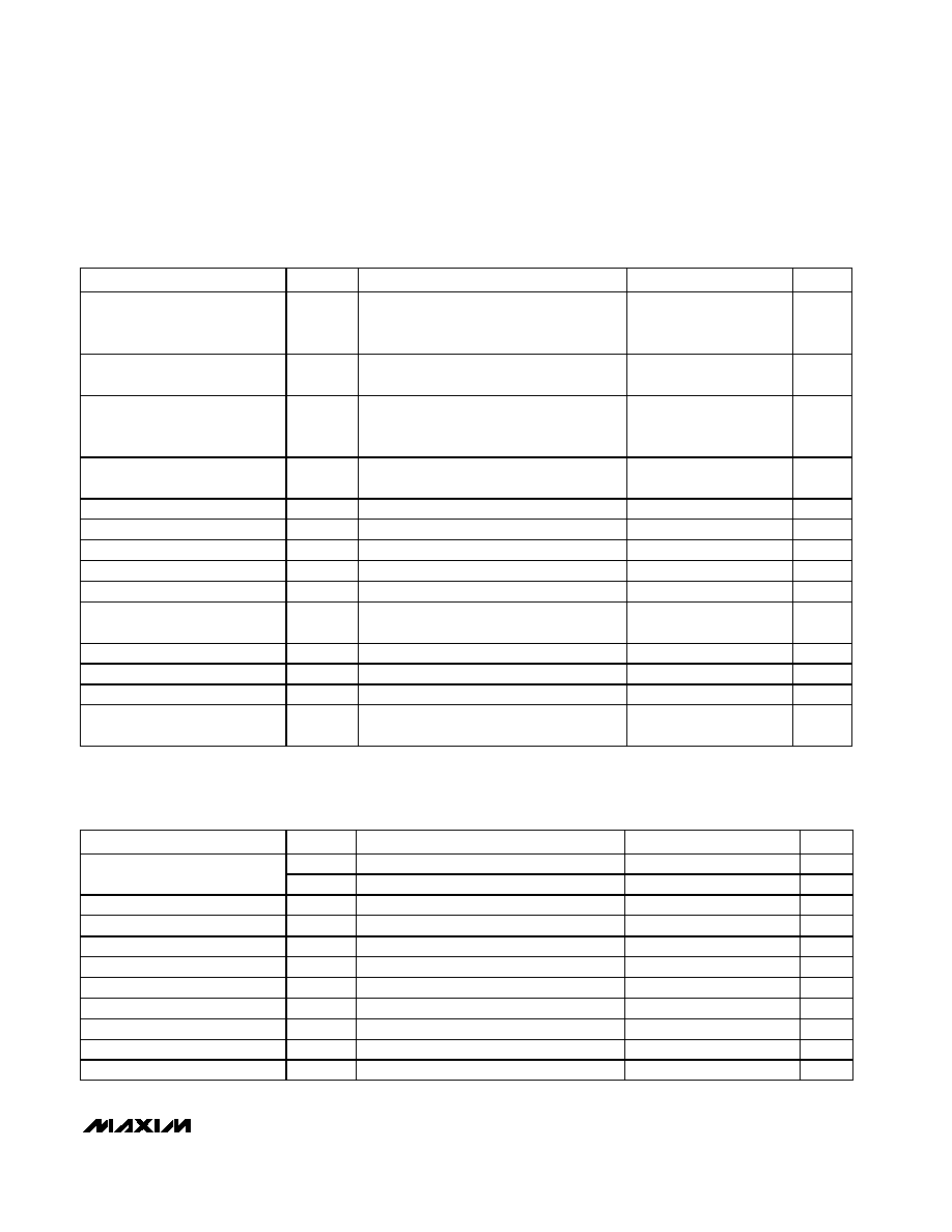
5
0
20
10
40
30
60
50
70
0
2
3
1
4
5
AUX QUIESCENT CURRENT vs. V
AUX
MAX1838 toc01
V
AUX
(V)
AUX QUIESCENT CURRENT (
µ
A)
V
IN
= 4.5V
V
IN
= 5V
V
IN
= 5.5V
SEL = GND
V
IN
= 0
0
10
5
20
15
25
30
0
2
3
1
4
5
IN QUIESCENT CURRENT vs. V
AUX
MAX1838 toc02
V
AUX
(V)
IN QUIESCENT CURRENT (
µ
A)
V
IN
= 4.5V
V
IN
= 5V
V
IN
= 5.5V
SEL = AUX
70
100
IN + AUX QUIESCENT CURRENT
vs. TEMPERATURE
MAX1838 toc03
TEMPERATURE (
∞C)
QUIESCENT CURRENT (
µ
A)
-40
20
40
-20
0
60
80
80
SEL = AUX = IN
90
V
AUX
= 4.5V
V
AUX
= 5V
V
AUX
= 5.5V
70
80
90
100
110
IN + AUX QUIESCENT CURRENT
vs. TEMPERATURE
MAX1838 toc04
TEMPERATURE (
∞C)
QUIESCENT CURRENT (
µ
A)
SEL = GND
V
IN
= V
AUX
= 5.5V
V
IN
= V
AUX
= 4.5V
V
IN
= V
AUX
= 5V
-40
20
40
-20
0
60
80
6.0
6.5
7.0
7.5
8.0
8.5
9.0
9.5
10.0
-40
0
-20
20
40
60
80
MAX1838 toc05
TEMPERATURE (
∞C)
SHUTDOWN CURRENT (
µ
A)
IN + AUX QUIESCENT SHUTDOWN CURRENT
vs. TEMPERATURE
V
IN
= V
AUX
= 5.0V
V
IN
= V
AUX
= 4.5V
V
IN
= V
AUX
= 5.5V
-40
80
TEMPERATURE (
∞C)
SWITCH LEAKAGE CURRENT (nA)
1
10
100
1000
0
20
-20
40
60
MAX1838 toc06
SWITCH LEAKAGE CURRENT
vs. TEMPERATURE, FULL DATA
IN = AUX = SEL = ON = GND
V
OUT_
= 5.5V
V
IN
= V
AUX
= V
ON
= V
SEL
= 5.5V
OUT_ = GND
0.7
0.9
0.8
1.1
1.0
1.2
1.3
-40
20
40
-20
0
60
80
MAX1838 toc07
TEMPERATURE (
∞C)
NORMALIZED ON-RESISTANCE (
)
NORMALIZED SWITCH ON-RESISTANCE
vs. TEMPERATURE
I
OUT_
= 500mA
0.86
0.88
0.90
0.92
0.94
MAX1838 toc08
TEMPERATURE (
∞C)
CONTINUOUS CURRENT LIMIT THRESHOLD (A)
-40
20
-20
0
40
60
80
CONTINUOUS CURRENT LIMIT THRESHOLD
vs. TEMPERATURE
1.8
1.9
2.1
2.0
2.2
2.3
-40
0
-20
20
40
60
80
TURN-ON DELAY vs. TEMPERATURE
MAX1838 toc09
TEMPERATURE (
∞C)
TURN-ON DELAY (ms)
SEL = GND
V
IN
= V
AUX
= 4.5V
V
IN
= V
AUX
= 5.0V
V
IN
= V
AUX
= 5.5V
Typical Operating Characteristics
(Circuit of Figure 2, V
IN_
= 5V, T
A
= +25
∞C, unless otherwise noted.)