 | –≠–ª–µ–∫—Ç—Ä–æ–Ω–Ω—ã–π –∫–æ–º–ø–æ–Ω–µ–Ω—Ç: MAX2247 | –°–∫–∞—á–∞—Ç—å:  PDF PDF  ZIP ZIP |

General Description
The MAX2247 low-voltage, three-stage linear power
amplifier (PA) is optimized for 802.11b/g wireless LAN
(WLAN) applications in the 2.4GHz ISM band. The
device is integrated with an adjustable bias control,
power detector, and shutdown mode. The MAX2247
features 29dB of power gain and delivers up to
+24dBm of linear output power at 24% efficiency from a
single +3.3V supply. It achieves less than -32dBc first-
side lobe suppression and less than -55dBc second-
side lobe suppression under 802.11b modulation. In
addition, the device can be matched for optimum effi-
ciency and performance at output power levels from
+10dBm to +24dBm. Its high +28dBm saturated output
power also allows the device to meet the requirements
of 802.11g OFDM modulation.
The MAX2247 features an external bias-control pin that
allows the supply current of the device to be dynamical-
ly throttled back at lower output power levels, thus
improving efficiency while maintaining sufficient side-
lobe suppression. Proprietary internal bias circuitry
maintains stable device performance over temperature
and voltage-supply variations. An additional power-sav-
ing feature is a logic-level shutdown pin that reduces
supply current to 0.5µA and eliminates the need for an
external supply switch. The integrated shutdown func-
tion also allows guaranteed device ramp-on and ramp-
off times.
The MAX2247 integrates a power detector with 20dB
dynamic range and ±0.8dB accuracy at the highest
output power level. The detector provides a buffered
DC voltage proportional to the output power of the
device, saving cost and space by eliminating a coupler
and op amp usually required to implement a power
detector function. The device is packaged in the tiny
3
4 chip-scale package (UCSPTM), measuring only
1.5mm
2mm, making it the ideal solution for radios built
in small form factors.
Applications
IEEE 802.11b DSSS WLAN
IEEE 802.11g OFDM WLAN
HomeRFTM
2.4GHz Cordless Phones
2.4GHz ISM Radios
Features
2.4GHz to 2.5GHz Operating Range
Up to +24dBm Linear Output Power (ACPR of
Less than -32dBc First-Side Lobe and Less than
-55dBc Second-Side Lobe)
24% PAE at +24dBm Linear Output Power, 3.3V
24% PAE at +21dBm Linear Output Power, 3.0V
29dB Power Gain
On-Chip Power Detector with Buffered Output
Internal 50 Input Matching
External Bias Control for Current Throttleback
Integrated Bias Circuitry
+2.7V to +4.2V Single-Supply Operation
0.5µA Shutdown Mode
Tiny Chip-Scale Package (1.5mm
2mm)
MAX2247
2.4GHz SiGe Linear Power Amplifier
________________________________________________________________
Maxim Integrated Products
1
Ordering Information
19-2520; Rev 4; 8/03
For pricing, delivery, and ordering information, please contact Maxim/Dallas Direct! at
1-888-629-4642, or visit Maxim's website at www.maxim-ic.com.
Typical Operating Circuit appears at end of data sheet.
PART
TEMP RANGE
PIN-
PACKAGE
TOP
MARK
MAX2247EBC-T
-40∞C to +85∞C
3
x
4 UCSP*
AAW
TOP VIEW
BIAS
A1
GND3
B1
RF_
OUT
C1
V
CC
2
A2
C2
GND2
A3
PD_
OUT
B3
V
CC
B
C3
V
CC
1
A4
GND1
B4
RF_IN
C4
MAX2247
SHDN
Pin Configuration
*Requires special solder temperature profile in the Absolute
Maximum Ratings Sections.
UCSP is a trademark of Maxim Integrated Products, Inc.
HomeRF is a trademark of HomeRF Working Group.

MAX2247
2.4GHz SiGe Linear Power Amplifier
2
_______________________________________________________________________________________
ABSOLUTE MAXIMUM RATINGS
DC ELECTRICAL CHARACTERISTICS
(MAX2247 EV kit, V
CC_
= +2.7V to +4.2V, SHDN = V
CC
, RF_IN and RF_OUT terminated to 50, T
A
= -40∞C to +85∞C. Typical values
are at +3V and T
A
= +25∞C, unless otherwise noted.) (Note 2)
Stresses beyond those listed under "Absolute Maximum Ratings" may cause permanent damage to the device. These are stress ratings only, and functional
operation of the device at these or any other conditions beyond those indicated in the operational sections of the specifications is not implied. Exposure to
absolute maximum rating conditions for extended periods may affect device reliability.
V
CC
1, V
CC
2, V
CC
B, RF_OUT to GND....................-0.3V to +4.5V
SHDN, BIAS, PD_OUT ................................-0.3V to V
CC_
+ 0.3V
RF Input Power (50 source)...........................................+5dBm
RF_IN Input Current............................................................±1mA
Maximum VSWR Without Damage ........................................10:1
Maximum VSWR for Stable Operation, P
OUT
< +25dBm........5:1
Continuous Power Dissipation (T
A
= +70∞C)
3
4 UCSP (derate 28.5mW/∞C above +70∞C) ..............1.3W
Thermal Resistance .........................................................35∞C/W
Operating Temperature Range ...........................-40∞C to +85∞C
Junction Temperature ......................................................+150∞C
Storage Temperature Range .............................-65∞C to +125∞C
Bump Temperature (soldering) (Note 1)
Infrared (15s) ...............................................................+220∞C
Vapor Phase (60s) .......................................................+215∞C
Continuous Operating Lifetime.....................10yrs ◊ 0.92
(T
A
- 60∞C)
(For Operating Temperature, T
A
+60∞C)
PARAMETER
CONDITIONS
MIN
TYP
MAX
UNITS
Supply Voltage
2.7
4.2
V
P
OUT
= +24dBm, V
CC_
= 3.3V
317
350
P
OUT
= +25dBm, V
CC_
= 4.2V
345
Idle current = 250mA
with V
CC
= 3.3V
P
OUT
= +23dBm, V
CC_
= 3.0V
305
P
OUT
= +21dBm with optimized output-matching circuit.
Refer to the MAX2247 EV kit for details.
175
P
OUT
= +18dBm with optimized output-matching circuit.
Refer to the MAX2247 EV kit for details.
120
Supply Current (Notes 3, 4)
P
OUT
= +15dBm with optimized output-matching circuit.
Refer to the MAX2247 EV kit for details.
85
mA
Shutdown Supply Current
SHDN = 0, no RF signal applied
0.5
10
µA
Digital Input Logic High
2
V
Digital Input Logic Low
0.8
V
Digital Input Current High
-1
+5
µA
Digital Input Current Low
-1
+1
µA
CAUTION! ESD SENSITIVE DEVICE

MAX2247
2.4GHz SiGe Linear Power Amplifier
_______________________________________________________________________________________
3
Note 1: This device is constructed using a unique set of packaging techniques that impose a limit on the thermal profile the device
can be exposed to during board-level solder attach and rework. This limit permits the use of only the solder profiles recom-
mended in the industry-standard specification, JEDEC 020A, paragraph 7.6, Table 3 for IR/VPR and convection reflow.
Preheating is required. Hand or wave soldering is not recommended.
Note 2: Characteristics are production tested at T
A
= +25∞C. DC specifications over temperature are guaranteed by design
and characterization.
Note 3: Idle current is controlled by external DAC for best efficiency over the entire output power range.
Note 4: Parameter is measured with RF modulation based on IEEE 802.11b standard.
Note 5: Minimum and maximum specifications are guaranteed by design and characterization.
Note 6: Operation outside this range is possible but not guaranteed.
Note 7: The total turn-on time required for PA output power to settle to within 0.5dB of the final value.
Note 8: Specification is corrected for PC board loss of approximately 0.3dB, on the output of the MAX2247 EV kit.
Note 9: Total turn-off time required for PA supply current to fall below 10µA.
Note 10: See the Typical Operating Characteristics for statistical variation.
AC ELECTRICAL CHARACTERISTICS
(MAX2247 EV kit, V
CC_
= +3V, f
RF
= 2.45GHz, SHDN = V
CC
, 50 RF system impedance, T
A
= +25∞C, unless otherwise noted.) (Note 5)
PARAMETER
CONDITIONS
MIN
TYP
MAX
UNITS
RF Frequency Range
(Notes 4, 6)
2.4 to 2.5
GHz
T
A
= +25∞C
26
29.5
V
CC_
= 3V, P
OUT
= +23dBm
T
A
= -40∞C to +85∞C
25
V
CC_
= 3.3V, P
OUT
= +24dBm
29.5
Power Gain (Notes 2, 4, 8)
V
CC_
= 4.2V, P
OUT
= +25dBm
30.5
dB
Gain Variation Over Supply
Voltage (Note 4)
V
CC
= 3.0V to 3.6V
±
0.5
dB
V
CC_
= 3V
22
23
V
CC_
= 3.3V
24
Output Power Over Temperature
(Notes 4, 8)
ACPR: First-side lobe < -32dBc,
second-side lobe < -55dBc
V
CC_
= 4.2V
25
dBm
Saturated Output Power
P
IN
= +5dBm
27.8
dBm
Harmonic Output (2f, 3f, 4f)
-45
dBc
Input VSWR
Over full P
IN
range
1.8:1
2.5:1
Output VSWR
Over full P
OUT
range
2:1
2.5:1
Power Ramp Turn-On Time
(Note 7)
0.8
1.5
µs
Power Ramp Turn-Off Time
(Note 9)
0.8
1.5
µs
RF Output Detector
Response Time
0.9
µs
P
OUT
= +23dBm
1
P
OUT
= +15dBm
0.6
RF Output Detector Voltage
(Note 10)
P
OUT
= +7dBm
0.47
V

MAX2247
2.4GHz SiGe Linear Power Amplifier
4
_______________________________________________________________________________________
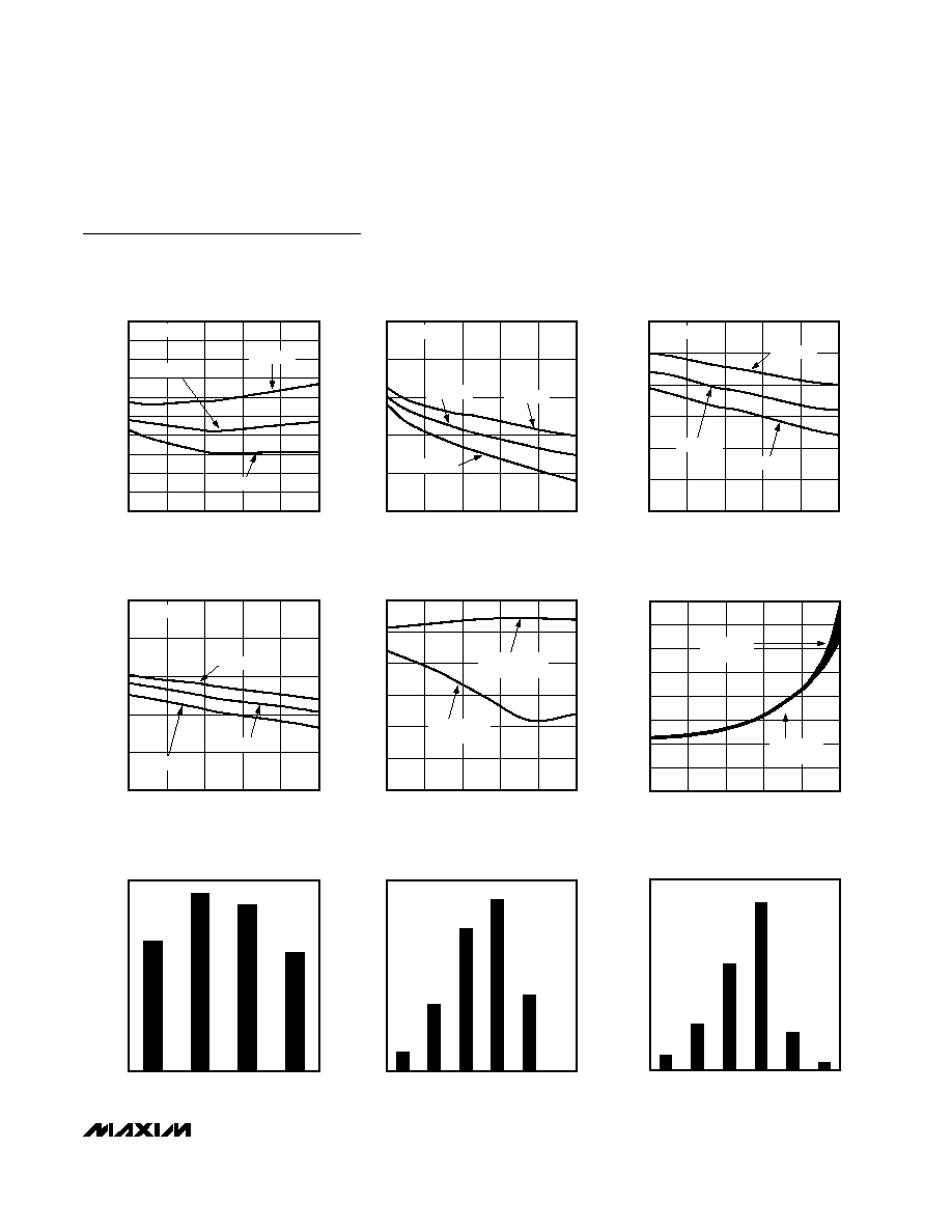
Typical Operating Characteristics
(V
CC_
= 3V, f
RF
= 2.45GHz, with MAX2247 EV kit optimized for P
OUT
= +23dBm. T
A
= +25∞C, unless otherwise noted.)
OUTPUT POWER, SUPPLY CURRENT
vs. SUPPLY VOLTAGE
MAX2247 toc01
SUPPLY VOLTAGE (V)
P
OUT
(dBm)
SUPPLY CURRENT (mA)
3.0
3.3
3.6
3.9
22
20
18
16
28
26
24
30
550
250
300
350
400
450
500
2.7
4.2
INPUT POWER ADJUSTED TO
KEEP ADJ/ALT CPR = -30dBc/-50dBc
T
A
= -40∞C
T
A
= +25∞C
T
A
= +85∞C
P
OUT
I
CC
OUTPUT POWER, SUPPLY CURRENT
vs. SUPPLY VOLTAGE
MAX2247 toc02
SUPPLY VOLTAGE (V)
P
OUT
(dBm)
SUPPLY CURRENT (mA)
3.0
3.3
3.6
3.9
22
20
18
16
28
26
24
14
550
250
300
350
400
450
500
2.7
4.2
T
A
= -40∞C
T
A
= +25∞C
T
A
= +85∞C
P
OUT
INPUT POWER ADJUSTED TO
KEEP ADJ/ALT CPR = -32dBc/-55dBc
I
CC
GAIN vs. SUPPLY VOLTAGE
MAX2247 toc03
SUPPLY VOLTAGE (V)
GAIN (dB)
3.9
3.6
3.3
3.0
26
27
28
29
30
31
32
33
34
35
25
2.7
4.2
P
OUT
= +23dBm
T
A
= -40∞C
T
A
= +25∞C
T
A
= +85∞C
SUPPLY CURRENT
vs. SUPPLY VOLTAGE
MAX2247 toc04
SUPPLY VOLTAGE (V)
SUPPLY CURRENT (mA)
3.9
3.6
3.3
3.0
260
270
280
290
300
310
320
330
340
350
250
2.7
4.2
P
OUT
= +23dBm
T
A
= -40∞C
T
A
= +25∞C
T
A
= +85∞C
ADJ CPR
vs. SUPPLY VOLTAGE
MAX2247 toc05
SUPPLY VOLTAGE (V)
ADJ CPR (dBc)
3.9
3.6
3.3
3.0
-38
-36
-34
-32
-30
-28
-26
-24
-40
2.7
4.2
P
OUT
= +23dBm
T
A
= -40∞C
T
A
= +25∞C
T
A
= +85∞C
ALT CPR
vs. SUPPLY VOLTAGE
MAX2247 toc06
SUPPLY VOLTAGE (V)
ALT CPR (dBc)
3.9
3.6
3.3
3.0
-64
-62
-60
-58
-56
-54
-52
-50
-48
-46
-66
2.7
4.2
P
OUT
= +23dBm
T
A
= -40∞C
T
A
= +25∞C
T
A
= +85∞C
OUTPUT POWER vs. INPUT POWER
MAX2247 toc07
P
IN
(dBm)
P
OUT
(dBm)
0
-5
-15
-10
5
10
15
20
25
30
35
40
0
-20
5
V
CC
= +4.2V
V
CC
= +3.3V
V
CC
= +3.0V
SUPPLY CURRENT vs. OUTPUT POWER
MAX2247 toc08
P
OUT
(dBm)
SUPPLY CURRENT (mA)
22
20
18
16
14
12
50
100
150
200
250
300
0
10
BIAS CURRENT ADJUSTED
TO KEEP ADJ/ALT CPR =
-32dBc/-55dBc
ADJ/ALT CPR vs. OUTPUT POWER
MAX2247 toc09
P
OUT
(dBm)
ADJ/ALT CPR (dBc)
22
20
14
16
18
12
-65
-60
-55
-50
-45
-40
-35
-30
-25
-20
-70
10
24
ADJ CPR
ALT CPR
MAX2247
2.4GHz SiGe Linear Power Amplifier
_______________________________________________________________________________________
5
ADJ CPR vs. FREQUENCY
MAX2247 toc10
FREQUENCY (MHz)
ADJ CPR (dBc)
2480
2460
2440
2420
-36
-35
-34
-33
-32
-31
-30
-29
-28
-27
-37
2400
2500
P
OUT
= +23dBm
T
A
= +25∞C
T
A
= +85∞C
T
A
= -40∞C
ALT CPR vs. FREQUENCY
MAX2247 toc11
FREQUENCY (MHz)
ALT CPR (dBc)
2480
2460
2440
2420
-58
-56
-54
-52
-50
-60
2400
2500
P
OUT
= +23dBm
T
A
= +25∞C
T
A
= +85∞C
T
A
= -40∞C
SUPPLY CURRENT vs. FREQUENCY
MAX2247 toc12
FREQUENCY (MHz)
SUPPLY CURRENT (mA)
2480
2460
2440
2420
270
280
290
300
310
320
260
2400
2500
P
OUT
= +23dBm
T
A
= +85∞C
T
A
= +25∞C
T
A
= -40∞C
GAIN vs. FREQUENCY
MAX2247 toc13
FREQUENCY (MHz)
GAIN (dB)
2480
2460
2440
2420
24
28
32
36
40
20
2400
2500
P
OUT
= +23dBm
T
A
= +85∞C
T
A
= +25∞C
T
A
= -40∞C
INPUT/OUTPUT RETURN LOSS
vs. FREQUENCY
MAX2247 toc14
FREQUENCY (MHz)
RETURN LOSS (dB)
2480
2460
2440
2420
-35
-25
-30
-20
-15
-10
-40
2400
2500
OUTPUT RETURN
LOSS
INPUT RETURN
LOSS
POWER DETECTOR VOLTAGE
vs. OUTPUT POWER
MAX2247 toc15
P
OUT
(dBm)
POWER DETECTOR VOLTAGE (V)
20
15
10
5
0.2
0.4
0.6
0.8
1.4
1.2
1.0
1.6
0
0
25
V
CC
= +2.7V,
T
A
= +85∞C
V
CC
= +4.2V,
T
A
= -40∞C
OUTPUT POWER HISTOGRAM AT FIXED
1V POWER DETECTOR VOLTAGE
MAX2247 toc16
OUTPUT POWER (dBm)
OCCURRENCES
23.375
22.625
22.875
23.125
2
4
6
8
10
12
14
16
0
SIGMA =
0.25dBm
BASED ON
50 PARTS
OUTPUT POWER HISTOGRAM AT FIXED
0.6V POWER DETECTOR VOLTAGE
MAX2247 toc17
OUTPUT POWER (dBm)
OCCURRENCES
15.593
15.356
15.119
14.882
14.645
14.408
5
10
15
20
0
SIGMA = 0.237dBm
BASED ON 50 PARTS
OUTPUT POWER HISTOGRAM AT FIXED
0.47V POWER DETECTOR VOLTAGE
MAX2247 toc18
OUTPUT POWER (dBm)
OCCURRENCES
7.95
7.57
7.19
6.81
6.43
6.05
5
10
15
20
0
SIGMA = 0.38dBm
BASED ON 50 PARTS
25
Typical Operating Characteristics (continued)
(V
CC_
= 3V, f
RF
= 2.45GHz, with MAX2247 EV kit optimized for P
OUT
= +23dBm. T
A
= +25∞C, unless otherwise noted.)