 | ÐлекÑÑоннÑй компоненÑ: MAX2266 | СкаÑаÑÑ:  PDF PDF  ZIP ZIP |
Äîêóìåíòàöèÿ è îïèñàíèÿ www.docs.chipfind.ru
General Description
The MAX2264/MAX2265/MAX2266 power amplifiers are
designed for operation in IS-98-based CDMA, IS-136-
based TDMA, and PDC cellular telephones operating in
the 900MHz range. When matched for CDMA operation
and biased with margin over the adjacent and alternate
channel specification (-45dBc/-56dBc), the amplifiers
achieve 28dBm output power with 37% efficiency
(MAX2265). At +16dBm output--a very common power
level for CDMA phones--the MAX2265 still has 7% effi-
ciency, yielding excellent overall talk time. At the same
power level, the MAX2264/MAX2266 have an unprece-
dented 12%/17% efficiency, while still obtaining
32%/32% efficiency at maximum output power.
The MAX2264/MAX2265/MAX2266 have internally refer-
enced bias ports that are normally terminated with sim-
ple resistors. The bias ports allow customization of
ACPR margin and gain. They can also be used to
"throttle back" bias current when generating low power
levels. The MAX2264/MAX2265/MAX2266 have excel-
lent gain stability over temperature (±0.8dB), so
overdesign of driver stages and excess driver current
are dramatically reduced, further increasing the
phone's talk time. The devices can be operated from
+2.7V to +5V while meeting all ACPR specifications
over the entire temperature range. Nonlinear efficiency
is 48% when matched for linear operation, or 55% when
matched for non-linear-only operation (MAX2265).
The devices are packaged in a 16-pin TSSOP with
exposed pad (EP). For module or direct chip attach
applications, the MAX2264 is also available in die form.
Applications
Cellular-Band CDMA Dual-Mode Phones
Cellular-Band PDC Phones
Cellular-Band TDMA Dual-Mode Phones
Dual-Mode Phones
2-Way Pagers
Power-Amplifier Modules
Features
o Low Average CDMA Current Consumption in
Typical Urban Scenario
55mA (MAX2264)
90mA (MAX2265)
40mA (MAX2266)
o 0.5µA Shutdown Mode Eliminates External
Supply Switch
o ±0.8dB Gain Variation Over Temperature
o No External Reference or Logic Interface
Circuitry Needed
o Supply Current and ACPR Margin
Dynamically Adjustable
o +2.7V to +5V Single-Supply Operation
o 37% Efficiency at +2.7V Operation
PART
For free samples & the latest literature: http://www.maxim-ic.com, or phone 1-800-998-8800.
For small orders, phone 1-800-835-8769.
MAX2264/MAX2265/MAX2266
2.7V, Single-Supply, Cellular-Band
Linear Power Amplifiers
________________________________________________________________ Maxim Integrated Products
1
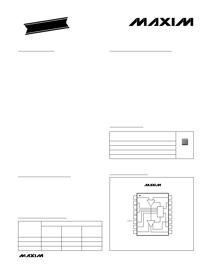
TOP VIEW
MAX2264/MAX2266
IN1
IN0
BIAS2H
V
CC
GND
NFP
OUT0
BIAS1L
OUT1
PWR
V
CC
SHDN
BIAS1H
V
CC
BIAS2L
OUT1
16
15
14
13
12
11
10
9
1
2
3
4
5
6
7
8
BIAS
TSSOP-EP
19-1524; Rev 2; 11/99
EVALUATION KIT MANUAL
FOLLOWS DATA SHEET
Pin Configurations
Ordering Information
Selector Guide
*Contact factory for dice specifications.
Pin Configurations continued at end of data sheet.
POWER-ADDED EFFICIENCY (%)
CDMA AT
+28dBm
CDMA AT
+16dBm
TDMA AT
+30dBm
--
42
7
12
32
37
MAX2265
MAX2264
DEVICE
16 TSSOP-EP
Dice*
16 TSSOP-EP
PIN-
PACKAGE
TEMP. RANGE
-40°C to +85°C
-40°C to +85°C
-40°C to +85°C
MAX2265EUE
MAX2264E/D
MAX2264EUE
16 TSSOP-EP
-40°C to +85°C
MAX2266EUE
--
17
32
MAX2266
TSSOP-EP
5mm x 6.4mm
MAX2264/MAX2265/MAX2266
2.7V, Single-Supply, Cellular-Band
Linear Power Amplifiers
2
_______________________________________________________________________________________
ABSOLUTE MAXIMUM RATINGS
DC ELECTRICAL CHARACTERISTICS
(V
CC
= +2.7V to +5V, T
A
= T
MIN
to T
MAX
, no input signal applied, V
SHDN
= 2.0V. Typical values are at V
CC
= +3.3V and T
A
= +25°C,
unless otherwise noted.)
Stresses beyond those listed under "Absolute Maximum Ratings" may cause permanent damage to the device. These are stress ratings only, and functional
operation of the device at these or any other conditions beyond those indicated in the operational sections of the specifications is not implied. Exposure to
absolute maximum rating conditions for extended periods may affect device reliability.
V
CC
to GND (no RF input) ....................................-0.3V to +6.5V
Logic Inputs to GND...................................-0.3V to (V
CC
+ 0.3V)
BIAS_ _ to GND ..........................................-0.3V to (V
CC
+ 0.3V)
RF Input Power .................................................+13dBm (20mW)
Logic Input Current...........................................................±10mA
Output VSWR with +13dBm Input ........................................2.5:1
Total DC Power Dissipation (T
PADDLE
= +100°C)
16-Pin TSSOP-EP (derate 60mW/°C
above T
PADDLE
= +100°C) ...............................................4W
JA ...............................................................................8°C/W
Operating Temperature Range ...........................-40°C to +85°C
Junction Temperature ......................................................+150°C
Storage Temperature Range .............................-65°C to +150°C
Lead Temperature (soldering, 10sec) .............................+300°C
AC ELECTRICAL CHARACTERISTICS--MAX2264
(MAX2264 EV kit, V
CC
= V
PWR
= V
SHDN
= +3.3V, T
A
= +25°C, f
IN
= 836MHz, CDMA modulation, SHDN = V
CC
, matching networks
tuned for 824MHz to 849MHz operation, 50
system, unless otherwise noted.)
PWR = GND
PWR = V
CC
PARAMETER
SYMBOL
MIN
TYP
MAX
UNITS
Logic Input Current Low
-1
1
µA
Logic Input Current High
-1
5
µA
Shutdown Supply Current
I
CC
0.5
10
µA
83
Logic Threshold High
2.0
V
Logic Threshold Low
0.8
V
Idle Current
Operating Voltage Range
V
CC
2.7
5.0
V
I
CC
95
34
CONDITIONS
Logic = GND
Logic = V
CC
SHDN = PWR = GND
MAX2265
MAX2264/MAX2266
mA
PARAMETER
SYMBOL
MIN
TYP
MAX
UNITS
Output Power
(Low-Power Mode) (Note 1)
P
OUT
15
16.5
dBm
26
27
Output Power
(High-Power Mode) (Note 1)
P
OUT
27
28
dBm
18
21
14
15.5
Power Gain (Note 1)
Frequency Range (Notes 1, 2)
f
IN
824
849
MHz
G
P
23
24.5
dB
22
CONDITIONS
PWR = GND, P
IN
adjusted to meet ACPR
specification, f
IN
= 824MHz to 849MHz
PWR = V
CC
= 2.8V, P
IN
adjusted to meet
ACPR specification, f
IN
= 824MHz to 849MHz
PWR = V
CC
, P
IN
adjusted to meet ACPR
specification, f
IN
= 824MHz to 849MHz
PWR = GND
PWR = GND, V
CC
= 2.8V, P
IN
adjusted to meet
ACPR specification, f
IN
= 824MHz to 849MHz
PWR = V
CC
or GND
PWR = V
CC
T
A
= +25°C
T
A
= T
MIN
to T
MAX
Gain Variation vs. Temperature
(Note 1)
±0.8
dB
T
A
= T
MIN
to T
MAX
, relative to T
A
= +25°C
MAX2264/MAX2265/MAX2266
2.7V, Single-Supply, Cellular-Band
Linear Power Amplifiers
_______________________________________________________________________________________
3
PARAMETER
SYMBOL
MIN
TYP
MAX
UNITS
AMPS Output Power (Note 1)
P
OUT
30.5
31
dBm
Adjacent-Channel Power Ratio
Limit (Notes 1, 2)
ACPR
-44
dBc
Alternate-Channel Power Ratio
Limit (Notes 1, 2)
ACPR
-56
dBc
AMPS Power-Added Efficiency
PAE
44
%
Power-Mode Switching Time
550
ns
Turn-On Time (Notes 1, 4)
1
5
µs
Maximum Input VSWR
VSWR
Nonharmonic Spurious due
to Load Mismatch (Notes 1, 5)
-60
dBc
Noise Power (Note 6)
-139
-136
AMPS Noise Power (Note 6)
-138
dBm/Hz
Harmonic Suppression
32
dBc
CONDITIONS
P
IN
= 8dBm
P
IN
= 8dBm
(Note 4)
V
CC
= 2.8V to 5.0V, offset = 885kHz,
30kHz BW, f
IN
= 824MHz to 849MHz
V
CC
= 2.8V to 5.0V, offset = 1980kHz,
30kHz BW, f
IN
= 824MHz to 849MHz
PWR = V
CC
or GND
f
IN
= 824MHz to 849MHz, PWR = GND or V
CC
P
IN
= 10dBm
Measured at 881MHz
PWR = GND, measured at 881MHz
Measured at 881MHz, P
IN
= 8dBm
(Note 7)
dBm/Hz
PARAMETER
SYMBOL
MIN
TYP
MAX
UNITS
26
26.5
Output Power (Note 1)
P
OUT
27
28
dBm
Gain Variation vs. Temperature
(Note 1)
±0.7
dB
AMPS Output Power (Note 1)
P
OUT
30
31
dBm
Adjacent-Channel Power Ratio
(Notes 1, 2)
ACPR
-44
-45
dBc
Alternate-Channel Power Ratio
(Notes 1, 2)
ACPR
-56
-57
dBc
Frequency Range (Notes 1, 2)
f
IN
824
849
MHz
23
CONDITIONS
V
CC
= 2.8V, P
IN
adjusted to meet ACPR
specification, f
IN
= 824MHz to 849MHz
P
IN
adjusted to meet ACPR specification,
f
IN
= 824MHz to 849MHz
T
A
= T
MIN
to T
MAX
, relative to T
A
= +25°C
P
IN
= 8dBm
V
CC
= 2.8V to 5.0V, offset = 885kHz,
30kHz BW, f
IN
= 824MHz to 849MHz
V
CC
= 2.8V to 5.0V, offset = 1980kHz,
30kHz BW, f
IN
= 824MHz to 849MHz
T
A
= T
MIN
to T
MAX
Power Gain (Note 1)
G
P
24
25.5
dB
T
A
= +25°C
AC ELECTRICAL CHARACTERISTICS--MAX2264 (continued)
(MAX2264 EV kit, V
CC
= V
PWR
= V
SHDN
= +3.3V, T
A
= +25°C, f
IN
= 836MHz, CDMA modulation, SHDN = V
CC
, matching networks
tuned for 824MHz to 849MHz operation, 50
system, unless otherwise noted.)
32
PWR = V
CC
, P
IN
adjusted to meet ACPR
specification
Power-Added Efficiency
(Note 3)
PAE
12
%
PWR = GND, P
IN
adjusted to meet ACPR
specification
AC ELECTRICAL CHARACTERISTICS--MAX2265
(MAX2265 EV kit, V
CC
= V
SHDN
= +3.3V, T
A
= +25°C, f
IN
= 836MHz, CDMA modulation, matching networks tuned for 824MHz to
849MHz operation, 50
system, unless otherwise indicated.)
2.4:1
MAX2264/MAX2265/MAX2266
2.7V, Single-Supply, Cellular-Band
Linear Power Amplifiers
4
_______________________________________________________________________________________
AC ELECTRICAL CHARACTERISTICS--MAX2265 (continued)
(MAX2265 EV kit, V
CC
= V
SHDN
= +3.3V, T
A
= +25°C, f
IN
= 836MHz, CDMA modulation, matching networks tuned for 824MHz to
849MHz operation, 50
system, unless otherwise indicated.)
PARAMETER
SYMBOL
MIN
TYP
MAX
UNITS
Power-Added Efficiency
(Note 3)
PAE
37
%
7
AMPS Power-Added Efficiency
PAE
48
%
Turn-On Time (Notes 1, 4)
1
5
µs
Maximum Input VSWR
VSWR
1.3:1
Nonharmonic Spurious Due
to Load Mismatch (Notes 1, 5)
-60
dBc
Noise Power (Note 6)
-140
dBm/Hz
AMPS Noise Power (Note 6)
-139
dBm/Hz
Harmonic Suppression
47
dBc
CONDITIONS
P
IN
adjusted to give P
OUT
= 28dBm
P
IN
adjusted for P
OUT
= 16dBm
P
IN
= 8dBm
f
IN
= 824MHz to 849MHz
P
IN
= 10dBm
Measured at 881MHz
Measured at 881MHz, P
IN
= 8dBm
(Note 7)
AC ELECTRICAL CHARACTERISTICS--MAX2266
(MAX2266 EV kit, V
CC
= V
SHDN
= +3.3V, T
A
= +25°C, f
IN
= 836MHz, CDMA modulation, matching networks tuned for 824MHz to
849MHz operation, 50
system, unless otherwise indicated.)
PARAMETER
SYMBOL
MIN
TYP
MAX
UNITS
Output Power
(Low-Power Mode) (Note 1)
P
OUT
14
15.5
dBm
26
27
Output Power
(High-Power Mode) (Note 1)
P
OUT
27
28
dBm
25
27.5
13
14
Power Gain (Note 1)
Frequency Range (Notes 1, 2)
f
IN
824
849
MHz
G
P
24.5
26
dB
23
CONDITIONS
PWR = GND, P
IN
adjusted to meet ACPR
specification, f
IN
= 824MHz to 849MHz
PWR = V
CC
= 2.8V, P
IN
adjusted to meet
ACPR specification, f
IN
= 824MHz to 849MHz
PWR = V
CC
, P
IN
adjusted to meet ACPR
specification, f
IN
= 824MHz to 849MHz
PWR = GND
PWR = GND, V
CC
= 2.8V, P
IN
adjusted to meet
ACPR specification, f
IN
= 824MHz to 849MHz
PWR = V
CC
or GND
PWR = V
CC
Gain Variation vs. Temperature
(Note 1)
±0.8
dB
T
A
= T
MIN
to T
MAX
, relative to T
A
= +25°C
T
A
= +25°C
T
A
= T
MIN
to T
MAX
Power-Added Efficiency
(Note 3)
PAE
32
%
17
PWR = V
CC
, P
IN
adjusted to meet ACPR
specification
PWR = GND, P
IN
adjusted to meet ACPR
specification
AMPS Output Power (Note 1)
P
OUT
31
32
dBm
P
IN
= 8dBm
Alternate-Channel Power Ratio
Limit (Notes 1, 2)
ACPR
-56
dBc
V
CC
= 2.8V to 5.0V, offset = 1980kHz,
30kHz BW, f
IN
= 824MHz to 849MHz
Adjacent-Channel Power Ratio
Limit (Notes 1, 2)
ACPR
-44
dBc
V
CC
= 2.8V to 5.0V, offset = 885kHz,
30kHz BW, f
IN
= 824MHz to 849MHz
MAX2264/MAX2265/MAX2266
2.7V, Single-Supply, Cellular-Band
Linear Power Amplifiers
_______________________________________________________________________________________
5
Note 1: Minimum and maximum values are guaranteed by design and characterization, not production tested.
Note 2: P
MAX
is met over this frequency range at the ACPR limit with a single matching network. For optimum performance at other
frequencies, the output matching network must be properly designed. See the Applications Information section. Operation
between 750MHz and 1000MHz is possible but has not been characterized.
Note 3: PAE is specified into a 50
load, while meeting ACPR requirements.
Note 4: Time from logic transition until P
OUT
is within 1dB of its final mean power.
Note 5: Murata isolator as load with 20:1 VSWR any phase angle after isolator.
Note 6: Noise power can be improved by using the circuit in Figures 1, 2, and 3.
Note 7: Harmonics measured on evaluation kit, which provides some harmonic attenuation in addition to the rejection provided by
the IC. The combined suppression is specified.
PARAMETER
SYMBOL
MIN
TYP
MAX
UNITS
AMPS Power-Added Efficiency
PAE
48
%
Power-Mode Switching Time
550
ns
Turn-On Time (Notes 1, 4)
1
5
µs
Maximum Input VSWR
VSWR
2.4:1
Nonharmonic Spurious due
to Load Mismatch (Notes 1, 5)
-60
dBc
Noise Power (Note 6)
-137
-130
AMPS Noise Power (Note 6)
-136
dBm/Hz
Harmonic Suppression
32
dBc
CONDITIONS
P
IN
= 8dBm
(Note 4)
PWR = V
CC
or GND
f
IN
= 824MHz to 849MHz, PWR = GND or V
CC
P
IN
= 10dBm
Measured at 881MHz
PWR = GND, measured at 881MHz
Measured at 881MHz, P
IN
= 8dBm
(Note 7)
dBm/Hz
AC ELECTRICAL CHARACTERISTICS--MAX2266 (continued)
(MAX2266 EV kit, V
CC
= V
PWR
= V
SHDN
= +3.3V, T
A
= +25°C, f
IN
= 836MHz, CDMA modulation, SHDN = V
CC
, matching networks
tuned for 824MHz to 849MHz operation, 50
system, unless otherwise noted.)
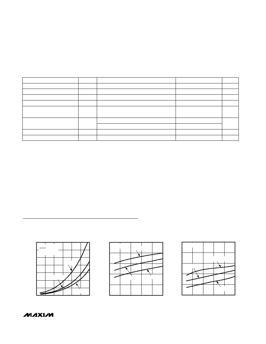
Typical Operating Characteristics
(MAX2264/MAX2265/MAX2266 EV kits, V
CC
= +3.3V, SHDN = V
CC
, CDMA modulation, T
A
= +25°C, unless otherwise noted.)
0
20
40
60
80
100
120
140
2.5
3.5
3.0
4.0
4.5
5.0
5.5
MAX2264
SHUTDOWN CURRENT vs. SUPPLY VOLTAGE
MAX2264-01
SUPPLY VOLTAGE (V)
SUPPLY CURRENT (nA)
T
A
= +85°C
T
A
= -40°C
T
A
= +25°C
PWR = GND
SHDN = GND
NO INPUT DRIVE
20
22
26
24
28
30
2.5
3.5
3.0
4.0
4.5
5.0
MAX2264
GAIN vs. SUPPLY VOLTAGE
MAX2264-02
SUPPLY VOLTAGE (V)
GAIN (dB)
PWR = V
CC
T
A
= -40°C
T
A
= +85°C
T
A
= +25°C
18
20
24
22
26
28
2.5
4.0
3.0
3.5
4.5
5.0
MAX2264
GAIN vs. SUPPLY VOLTAGE
MAX2264-03
SUPPLY VOLTAGE (V)
GAIN (dB)
PWR = GND
T
A
= -40°C
T
A
= +85°C
T
A
= +25°C