MAX2306/8/9EV Kit
General Description
The MAX2306/MAX2308/MAX2309 evaluation kits (EV
kits) simplify testing of the MAX2306/MAX2308/
MAX2309 IF receivers. These kits allow evaluation of
the devices' variable-gain amplifier (VGA), I/Q demodu-
lator, dual-band voltage-controlled oscillators (VCOs),
synthesizer, 3-wire programming interface, and power-
management features.
The EV kits provide 50
SMA connectors for all signal
inputs and outputs. A varactor-based tank circuit is pro-
vided for the on-chip VCO and can be tuned by a
potentiometer or an external voltage or phase-locked
with the on-chip phase-locked loop (PLL).
Features
o Dual Oscillators (MAX2306)
o On-Board PLL Synthesizer
o 3-Wire Interface
o Single-Ended or Differential Baseband Outputs
o +2.7V to +5.5V Single-Supply Operation
o SMA Connectors on All Signal Ports
o PC Control Software (available at
www.maxim-ic.com)
Evaluate: MAX2306/MAX2308/MAX2309
MAX2306/MAX2308/MAX2309 Evaluation Kits
________________________________________________________________ Maxim Integrated Products
1
19-2109; Rev 0; 7/01
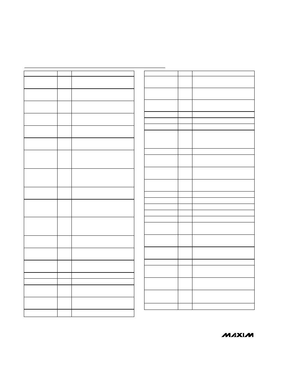
Component List
Ordering Information
PART
TEMP. RANGE
IC PACKAGE
MAX2306EVKIT
-40°C to +85°C
28 QSOP-EP*
MAX2308EVKIT
-40°C to +85°C
28 QSOP-EP*
MAX2309EVKIT
-40°C to +85°C
28 QSOP-EP*
*Exposed pad
For pricing, delivery, and ordering information, please contact Maxim/Dallas Direct! at
1-888-629-4642, or visit Maxim's website at www.maxim-ic.com.
DESIGNATION
QTY
DESCRIPTION
C1, C33, C34
3
47pF
±10%, 25V min ceramic
capacitors (0402)
C2
1
2pF
±0.1pF, 25V min ceramic
capacitor (0402) (MAX2306)
C3
1
33pF
±10%, 25V min ceramic
capacitor (0402) (MAX2306)
C4
1
33pF
±10%, 25V min ceramic
capacitor (0402)
(MAX2306/MAX2309)
C5
1
2pF
±0.1pF, 25V min ceramic
capacitor (0402)
(MAX2306/MAX2308)
C6
1
33pF
±10%, 25V min ceramic
capacitor (0402)
C7
1
33pF
±10%, 25V min ceramic
capacitor (0402)
(MAX2306/MAX2308)
C8, C12, C23,
C24, C25, C31
6
330pF
±10%, 25V min ceramic
capacitors (0402)
DESIGNATION
QTY
DESCRIPTION
C9, C10, C11,
C13, C14, C15,
C21, C22, C28,
C30, C35, C37,
C38, C42, C46,
C57, C59
15
0.01µF
±10%, 25V min ceramic
capacitors (0402)
C16
1
3.0pF
±0.1pF, 25V min ceramic
capacitor (0402)
(MAX2306/MAX2308)
C18
1
0.01µF
±1%, 25V min ceramic
capacitor (0402)
(MAX2306/MAX2308)
C19, C20
2
10pF
±10%, 25V min ceramic
capacitors (0402)
C27, C56, C58
3
10µF
±10%, 16V min tantalum
capacitors
AVX TAJC106K016
C29
1
0.068µF
±10%, 25V min ceramic
capacitor (0402)
C36
0
Open
C43
1
1000pF
±10% capacitor (0402)
(MAX2309)
DESIGNATION
QTY
DESCRIPTION
R5
10k
±5% resistor (0402)
(MAX2306/MAX2308)
R6
1
100
±5% resistor (0402)
(MAX2306/MAX2309)
R8, R14, R16,
R18
4
100
±5% resistors (0402)
R7
1
49.9
±1% resistor (0402)
R9
1
681
±1% resistor (0402)
R10
1
4.7k
±5% resistor (0402)
R11, R19, R31,
R32, R33, R34,
R40, R81
8
5k
±5% resistors (0402)
R12, R22
2
47k
±5% resistors (0402)
R13, R24
2
10k
Bourns variable resistors,
Digi-Key 3296W-104-ND
R15, R17
2
100
±5% resistors (0402)
(MAX2309)
R20, R21, R25,
R35
0
Open
R23
1
2.4k
±5% resistor (0402)
R26
1
47k
±5% resistor (0402)
R41
1
0
resistor (0402) (MAX2306)
R44
1
0
resistor (0402) (MAX2309)
J18
1
20-pin header
JU3, JU9,
JU10, JU11
4
Two-pin headers
T1
1
Balun transformer,
Toko DB458-1011
U1
1
MAX2306EGI, MAX2308EGI, or
MAX2309EGI IC
U2, U3
2
MAX4108ESA
None
1
MAX2306/MAX2308/MAX2309
circuit board
None
1
MAX2306/MAX2308/MAX2309
data sheet
INTF2300
Interface Board
1
3-wire programming and
interface board
None
1
20-pin ribbon cable
DESIGNATION
QTY
DESCRIPTION
C44, C47C53
8
0.1µF
±10%, 25V min ceramic
capacitors (0402)
C54, C55
2
0.1µF
±10%, 25V min ceramic
capacitors (0805)
C60
1
0
resistor (0402)
(MAX2309)
C61
1
2pF
±0.1pF, 25V min ceramic
capacitor (0402) (MAX2309)
D2
1
Varactor diode (MAX2306)
Alpha SMV1763-079
D3
1
Varactor diode
Alpha SMV1763-079
D4
1
Varactor diode
(MAX2306/MAX2308)
Alpha SMV1763-079
D5
1
Varactor diode
(MAX2306/MAX2309)
Alpha SMV1763-079
L1
1
33nH inductor (MAX2306)
Coilcraft 0603CS-33NXGBC
L2
1
33nH inductor
(MAX2306/MAX2308)
Coilcraft 0603CS-33NXGBC
L3
1
120nH inductor
(MAX2306/MAX2308)
Coilcraft 0603CS-33NXGBC
L4
1
220nH inductor
Coilcraft 0603CS-R22TKBC
L5
1
33nH inductor (MAX2309)
Coilcraft 0603CS-33NXGBC
L6
1
270nH inductor
Toko LL1608-PSR275
Q1
1
Open
R1, R38, R39
3
0
resistors (0402)
R2
1
10k
±5% resistor (0402)
(MAX2306)
R3
1
10k
±5% resistor (0402)
(MAX2306/MAX2309)
R4
1
10k
±5% resistor (0402)
Evaluate: MAX2306/MAX2308/MAX2309
MAX2306/MAX2308/MAX2309 Evaluation Kits
2
_______________________________________________________________________________________
Component List (continued)
Quick Start
The MAX2306/MAX2308/MAX2309 EV kits are fully
assembled and factory tested. Follow the instructions in
the Connections and Setup section.
Recommended Test Equipment
The test equipment recommended to verify MAX2306/
MAX2308/MAX2309 operation is listed in Table 1. This list
is intended as a guide only; substitutions may be possible.
Connections and Setup
The following sections provide instructions for getting
the EV kit running in CDMA mode.
CDMA Mode
Perform the following steps to evaluate the MAX2306/
MAX2308/MAX2309 in CDMA mode:
1) Verify that shunts JU3, JU10, and JU11 are in place.
2) Connect the INTF2300 interface cable as shown in
Figure 11. (Pin 1 of the interface cable corresponds
to the red wire; pin 1 is designated in silkscreen on
each of the PC boards.)
3) Connect a +2.75V power supply to the VCC and
GND terminals. Set the other two supplies to +5V
and -5V and then connect to the appropriate +5V,
-5V, and GND terminals on the EV board.
4) Install and run Maxim's CDMA control software
(available at www.maxim-ic.com). Under the
Technical Support heading, click on SOFTWARE.
Select the correct software to download and install.
5) With the MAX2306, MAX2308, or MAX2309 screen
active, set the control pins. Set SHDN to "H". On the
MAX2306, set the MODE to "H". On the MAX2309,
set STBY, BUF_EN, and DIVSEL to "H". Turn on the
power supplies. Under Preset Modes select CDMA
mode. Under Program Dividers set M1 and M2 to
306. Set R1 and R2 to 16 and then click Send Data
for M1, M2, R1, and R2. Under Control Register,
click on Send Data.
6) Connect a signal generator to the REF port, config-
ured for a sine wave with a 19.2MHz frequency and a
-10dBm amplitude. (The REF port is 50
terminated.)
7) Connect a signal generator with 183.72MHz at
-66dBm and apply it to the CDMA differential port.
8) Set VGC to 2.5VDC by rotating potentiometer R13.
Optionally, an external VGC voltage may be used
by removing jumper JU3 and applying a DC volt-
age to JU3 at the pin labeled VGC.
9) Configure an oscilloscope to measure a high-
impedance, 1Vp-p, 100kHz waveform. Connect it to
the I or Q output.
Voltage gain can be calculated by:
Gain = approximately 60dB
Note: The balun loss is not taken into account. This loss
is typically less than 0.5dB. There may also be some
loss through the MAX4108 op amp.
V (RMS)
5
10
P (dBm) - 30
10
IN
=
×
IN
00
Gain
20log
V
2 2
OUTp-p
=
V
IN
Evaluate: MAX2306/MAX2308/MAX2309
MAX2306/MAX2308/MAX2309 Evaluation Kits
_______________________________________________________________________________________
3
Component Suppliers
Windows95 and Windows are registered trademarks
of Microsoft Corp.
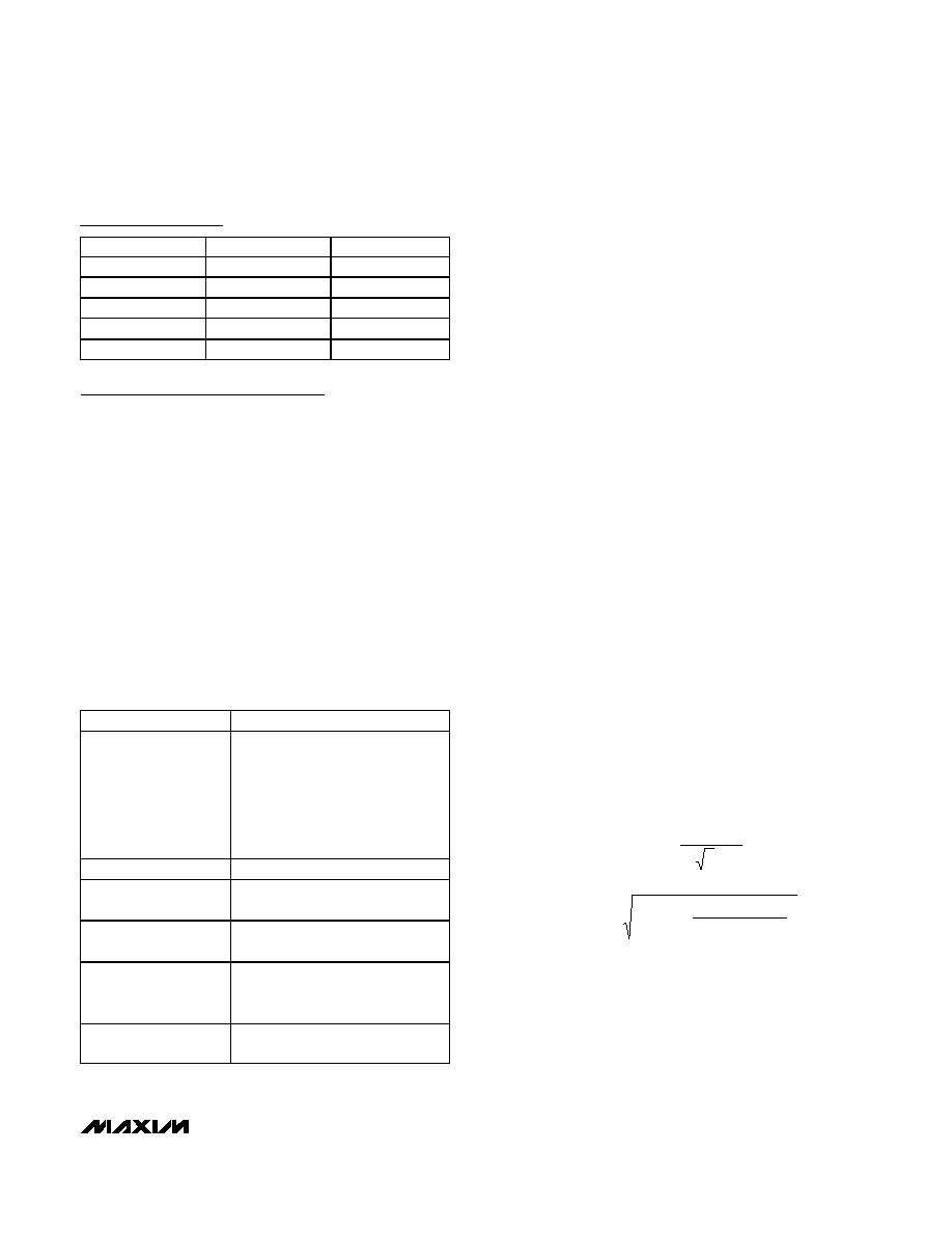
Table 1. Recommended Equipment
SUPPLIER
PHONE
FAX
Alpha Industries
617-935-5150
617-933-2359
AVX
803-946-0690
803-626-3123
Coilcraft
847-639-6400
847-639-1469
Murata
770-436-1300
770-436-3030
Toko
708-297-0070
708-699-1194
EQUIPMENT
DESCRIPTION
RF Signal
Generators (2)
HP 8648A or equivalent. Capable of
delivering -70dBm to -10dBm of
output power in the 10MHz to
500MHz frequency range. One
generator is required to test the
receive signal path and the other is
for the reference frequency.
Oscilloscope
For viewing the demodulator outputs.
Power Supply (3)
Capable of providing at least 100mA
at +2.7V to +5.5V.
Additional Voltage
Source
For external control of VGA (optional).
Personal Computer
486DX33 or better, with Windows95
®
or later version of Windows
®
operating system and a parallel port.
INTF2300 Interface
Board
Provided with EV kit.

Evaluate: MAX2306/MAX2308/MAX2309
Adjustments and Control
VGC Adjust
The MAX2306/MAX2308/MAX2309 EV kits are config-
ured with a 10k
trim pot for setting and adjusting the
VGA gain. An external supply can be used by removing
the 2-pin shunt (JU3) and by directly connecting the sup-
ply to JU3 at pin labeled VGC. The VGC voltage must be
clean to minimize undesired amplitude modulation.
Interface Control
The interface port is designed to use a 20-pin ribbon
cable. Ten pins are signal lines, and the other ten pins
are digital grounds. Pin 1 of the interface cable is red.
Pin 1 is also designated in silkscreen on each of the PC
boards.
Detailed Description
The following sections cover the EV kits' circuit blocks
in detail. (Refer to the MAX2306/MAX2308/MAX2309
data sheet for additional information.)
CDMA Inputs
The on-board balun converts the CDMA DIFF input to a
differential signal for the MAX2306/MAX2308/MAX2309.
The 50
source impedance is transformed to 500 by
the combination of L4, R9, C19, C20, and the 4:1
impedance ratio of the input balun.
FM Inputs
The EV kit is configured for single-ended (50
) opera-
tion at the FM connector. The matching network trans-
forms 50
to 850.
REF Inputs
The REF port is AC-coupled and terminated for use
with a 50
signal source.
I/Q Outputs
The I/Q outputs are self-biased baseband outputs. The
differential I/Q outputs are converted to single-ended
outputs with MAX4108 op amps.
PC Board Layout/
Construction
The MAX2306/MAX2308/MAX2309 EV kits can serve as
board layout guides. Keep PC board trace lengths as
short as possible to minimize parasitics. Keep decou-
pling capacitors close to the device, with a low-induc-
tance through connection to the ground plane.
INTF2300
Interface Board
The INTF2300 interface board is used to control the 3-
wire interface of a device under test from the parallel
port of a PC. This board level translates 5V logic from
the PC to VCC of the device under test. The INTF2300
also provides buffering and EMI filtering. The recom-
mended operating supply voltage range is +2.7V to
+3.6V. For operation of the MAX2306/MAX2309 above
+3.6V, jumper JU1 may be removed and an external
supply voltage of +3.6V may be applied between VCC
(pin 2) and GND (pin 1) (Figure 11).
MAX2306/MAX2308/MAX2309 Evaluation Kits
4
_______________________________________________________________________________________
Evaluate: MAX2306/MAX2308/MAX2309
MAX2306/MAX2308/MAX2309 Evaluation Kits
_______________________________________________________________________________________
5
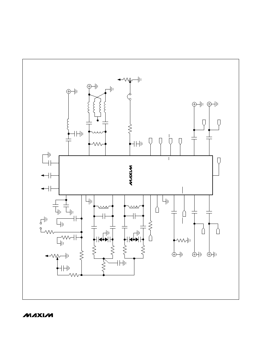
Figure 1. MAX2306EV Kit Schematic
MAX2306
BYP
FM+
BYP
R10
4.7k
R1
0
R3
10k
R2
10k
C4
33pF
C3
33pF
C1
47pF
C46
0.01
µ
F
L1
33nH
L2
33nH
C2
2pF
C29
0.068
µ
F
C30
0.01
µ
F
R23
2.4k
CP_OUT
GND
TANKL+
TANKL-
MODE
V
CC
VGC
CDMA-
CDMA+
VCC
DATA
CLK
GND
REF
R5
10k
D3
D4
R4
10k
C7
33pF
C6
33pF
C5
2pF
TANKH+
TANKH-
D3
D4
D2
D5
V
CC
VCCD
MODE/DIVSEL
5
6
7
4
3
2
1
28
25
26
27
SHDN
J3
C10
0.01
µ
F
REF
J15
IOUT+
J12
IOUT-
R7
49.9
C9
0.01
µ
F
RXI-
C11
0.01
µ
F
14
15
16
18
19
20
21
24
C13
0.01
µ
F
C14
0.01
µ
F
C15
0.01
µ
F
23
22
R13
10k
JU3
R12
47k
TOKO
4458D8-1011
C18
0.01
µ
F
L3
120nH
C19
10pF
C20
10pF
C16
3.0pF
R9
681
L4
220nH
J4
CDMA DIFF
FM
J5
T1
C21
0.01
µ
F
13
12
11
LOCK
J14
QOUT-
CLK
LOCK
RXQ-
DATA
VCCA
VCCA
VCCA
J13
QOUT+
C22
0.01
µ
F
C35
0.01
µ
F
8
IOUT+
9
IOUT-
QOUT-
10
QOUT+
BYP
FM-
SHDN
R35
OPEN
JU9
VCC
R24
10k
C36
OPEN
R25
OPEN
17
RXI+
RXQ+
EN
EN
C31
330pF
R41
0
U1