
General Description
The MAX2310/MAX2314 evaluation kits (EV kits) simpli-
fy testing of the MAX2310/MAX2314 IF receivers. These
kits allow evaluation of the devices' variable-gain ampli-
fier (VGA), I/Q demodulator, dual-band voltage-con-
trolled oscillators (VCOs), synthesizer, 3-wire program-
ming interface and power-management features.
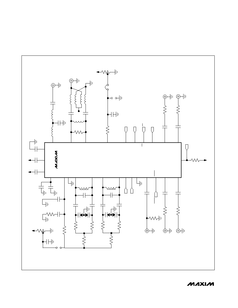
Figures 1 and 2 show MAX2310 and MAX2314 kit
schematics, respectively.
The EV kits provide 50
SMA connectors for all signal
inputs and outputs. A varactor-based tank circuit is pro-
vided for the on-chip VCO and can be tuned by a
potentiometer or an external voltage or phase locked
with the on-chip phase-locked loop (PLL). PC board
pads (J12, J13, J14, J15) are available for installing
low-inductance oscilloscope probe points, if desired.
Features
o 3-Wire Interface
o Differential Baseband Outputs
o +2.7V to +5.5V Single-Supply Operation
o SMA Connectors on All Signal Ports
o Low-Power Shutdown Mode
o PC Control Software (available at
www.maxim-ic.com)
Evaluate: MAX2310/MAX2314
MAX2310/MAX2314 Evaluation Kits
________________________________________________________________ Maxim Integrated Products
1
19-1507; Rev 1; 12/00
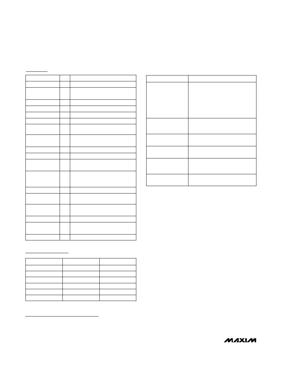
Component List
PART
MAX2310EVKIT
MAX2314EVKIT
-40∞C to +85∞C
-40∞C to +85∞C
TEMP. RANGE
IC PACKAGE
28 QSOP
28 QSOP
Ordering Information
8pF ±10%, 25V min ceramic
capacitors (0402)
2
C19, C20
0.01µF ±10%, 25V min ceramic
capacitors (0402)
15
C9, C10, C11,
C13, C14, C15,
C18, C21, C22,
C28, C35, C37,
C38, C42, C46
330pF ±10%, 25V min ceramic
capacitors (0402)
5
C8, C12, C23,
C24, C25
12pF ±10%, 25V min ceramic
capacitors (0402) (MAX2310)
2
C6, C7
Open
9
C16, C26, C31,
C32, C36, C39,
C40, C41, C45
1.5pF ±0.1pF, 25V min ceramic
capacitor (0402) (MAX2310)
1
C5
18pF ±10%, 25V min ceramic
capacitors (0402)
2
C3, C4
DESIGNATION
5pF ±0.1pF, 25V min ceramic
capacitor (0402)
1
C2
47pF ±10%, 25V min ceramic
capacitors (0402)
3
C1, C33, C34
DESCRIPTION
QTY
10pF ±10%, 25V min ceramic
capacitor (0402)
1
C17
Note: To evaluate the MAX2312 or MAX2316, order the
MAX2312EVKIT or MAX2316EVKIT.
0.033µF ±10%, 25V min ceramic
capacitor (0402)
1
C29
Varactor diode
Alpha SMV1255-003
1
D3
Open
1
D1
Varactor diode (MAX2310)
Alpha SMV1255-003
1
D4
3300pF ±10%, 25V min ceramic
capacitor (0402)
1
C30
DESIGNATION
DESCRIPTION
QTY
10µF ±10%, 16V min tantalum cap
AVX TAJC106K016
1
C27
270nH inductor
Coilcraft 0805CS-271 XKBC
1
L5
180nH inductor
Coilcraft 0805CS-181TKBC (MAX2310)
1
L4
1µH inductor
Coilcraft 1008CS-102 XKBC
1
L3
18nH inductor (MAX2310)
Coilcraft 0805CS-220 XJBC
1
L2
68nH inductor
Coilcraft 0805CS-680 XJBC
1
L1
3-wire programming and interface
board
1
INTF2300
Interface Board
680nH inductor
Coilcraft 0805CS-681TKBC (MAX2314)
For pricing, delivery, and ordering information, please contact Maxim/Dallas Direct! at
1-888-629-4642, or visit Maxim's website at www.maxim-ic.com.
Evaluate: MAX2310/MAX2314
MAX2310/MAX2314 Evaluation Kits
2
_______________________________________________________________________________________
Quick Start
The MAX2310/MAX2314 EV kits are fully assembled
and factory tested. Follow the instructions in the
Connections and Setup section.
Recommended Test Equipment
The test equipment recommended to verify MAX2310/
MAX2314 operation is listed in Table 1. This list is
intended as a guide only; substitutions may be possi-
ble.
Connections and Setup
The following sections provide instructions for getting
the EV kit running in both the CDMA and FM modes.
CDMA Mode
Perform the following steps to evaluate the MAX2310/
MAX2314 in CDMA mode:
1) Verify that shunts JU3, JU10, and JU11 are in place.
2) Connect the INTF2300 interface cable as shown in
Figure 8. (Pin 1 of the interface cable corresponds
to the red wire; pin 1 is designated in silk screen on
each of the PC boards.)
3) Connect a +2.75V power supply to the V
CC
and
GND terminals.
4) Install and run Maxim's CDMA control software
(available at www.maxim-ic.com). Click on the
Maxim CDMA software on the Windows task bar.
On the IC selection form, click on the MAX2310/
MAX2314 control button.
EQUIPMENT
DESCRIPTION
RF Signal
Generators (2)
HP 8648A or equivalent. Capable of
delivering -70dBm to -10dBm of out-
put power in the 10MHz to 500MHz
frequency range. One generator is
required to test the receive signal
path and the other is for the refer-
ence frequency.
Component List (continued)
Oscilloscope
For viewing the demodulator out-
puts, 3-wire serial interface, and
other functions
Power Supply
Capable of providing at least 100mA
at +2.7V to +5.5V
Additional Voltage
Source
For external control of VGA functions
(optional)
Personal Computer
486DX33 or better, with Windows95
Æ
or Windows98
Æ
operating system and
a functional parallel port.
INTF2300 Interface
Board
Provided with EV kit
SUPPLIER
PHONE
FAX
Alpha Industries
617-935-5150
617-933-2359
AVX
803-946-0690
803-626-3123
Coilcraft
847-639-6400
847-639-1469
Digi-Key
218-681-6674
218-681-3380
Murata
949-852-2001
949-852-2002
Toko
708-297-0070
708-699-1194
Component Suppliers
Windows95 and Windows98 are registered trademarks
of Microsoft Corp.
Open
1
Q1
0
resistors (0402)
6
R1, R10, R12,
R31≠R34
47k
±5% resistors (0402)
2
R22, R26
10k
Bourns variable resistors
Digi-Key 3296W-104-ND
2
R13, R24
680
±1% resistor (0402)
1
R9
49.9
±1% resistor (0402)
1
R7
100
±5% resistors (0402)
4
R8, R14, R16,
R18
10k
±5% resistors (0402)
3
R2, R3, R23
DESIGNATION
DESCRIPTION
QTY
Open
11
R15, R17, R19,
R20, R21, R25,
R27≠R30, R35
Maxim MAX2310EEI or
MAX2314EEI IC
1
U1
MAX2310/MAX2314 circuit board
1
None
MAX2310/MAX2312/MAX2314/
MAX2316 data sheet
1
None
20-pin ribbon cable
1
None
Balun transformer
Toko DB458-1011
1
T1
Table 1. Recommended Equipment
0
resistors (0402) (MAX2310)
1
R11
10k
±5% (0402) (MAX2310)
2
R4, R5
1000pF ±10% (0402) (MAX2314)
1
C43
100
±5% resistor (0402)
(MAX2310)
1
R6

Evaluate: MAX2310/MAX2314
MAX2310/MAX2314 Evaluation Kits
_______________________________________________________________________________________
3
5) With the MAX2310/MAX2314 control screen active,
bring the SHDN pin high by clicking on the "H" con-
trol button located near the middle of the screen.
6) (MAX2310 only) With the MAX2310/MAX2314 con-
trol screen active, bring the MODE pin high by
clicking on the "H" control button located near the
middle of the screen. The mode pin is floated on
the MAX2314 board. In the control register set the
DIV_SEL bit and the VCO_SEL bit to "0." Click on
the "send data" button.
7) Connect a function generator to the REF port, con-
figured for a sine wave with a 19.68MHz frequency
and a -10dBm amplitude. (The REF port is 50
ter-
minated.)
8) Connect a signal generator with 210.48MHz
(MAX2310) or 85.48MHz (MAX2314) at -66dBm and
apply it to the CDMA differential port.
9) Set VGC to 2.5VDC by rotating potentiometer R13.
Optionally, an external VGC voltage may be used
by removing jumper JU3 and applying a DC volt-
age to JU2.
10) Configure an oscilloscope to measure a high-
impedance (10k
), 1Vp-p, 100kHz differential
waveform. Connect it to the I or Q output.
Voltage gain can be calculated by:
Gain = approximately 60dB
Note: The balun loss is not taken into account. This loss
is typically less than 0.5dB.
FM Mode
Perform the following steps to change to FM mode:
1) With the MAX2310/MAX2314 control screen active,
bring the MODE pin low by clicking on the "L" con-
trol button located near the middle of the screen
(MAX2310). Set the IN_SEL bit to "0." Click on the
"send data" button (MAX2314).
2) Connect a signal generator with 85.48MHz at -66dBm
and apply it to the FM port.
3) Configure an oscilloscope to measure a high-
impedance (10k
), 1Vp-p, 100kHz, differential
waveform. Connect it to the I or Q output.
Adjustments and Control
VGC Adjust
The MAX2310/MAX2314 EV kits are configured with a
10k
trim pot for setting and adjusting the VGA gain.
An external supply can be used by removing the 2-pin
shunt (JU3) and by directly connecting the supply to
JU2. The VGC voltage must be clean to minimize unde-
sired amplitude modulation.
Interface Control
The interface port is designed to use a 20-pin ribbon
cable. Ten pins are signal lines, and the other 10 pins
are digital grounds. Pin 1 of the interface cable is red.
Pin 1 is also designated in silk screen on each of the
PC boards.
Detailed Description
The following sections cover the EV kits' circuit blocks
in detail. (Refer to the MAX2310/MAX2312/MAX2314/
MAX2316 data sheet for additional information.)
CDMA Inputs
The CDMA+ and CDMA- pins are differential inputs to
the VGAs of the MAX2310/MAX2314. The EV kit is con-
figured for single-ended (50
) operation at the CDMA
differential input connector. The on-board balun con-
verts this input to a differential signal for the
MAX2310/MAX2314. The impedance is set by the com-
bination of L4, R9, C19, C20, and the 4:1 impedance
ratio of the input balun.
FM Inputs
The FM+ and FM- pins are differential inputs to the
VGAs of the MAX2310/MAX2314. The EV kit is config-
ured for single-ended (50
) operation at the FM con-
nector. The matching network transforms 50
to 850.
REF Inputs
The REF port is AC-coupled and terminated for use
with a 50
signal source.
I/Q Outputs
The I/Q outputs are self-biased baseband outputs.
PC Board Layout/Construction
The MAX2310/MAX2314 EV kits can serve as board
layout guides. Keep PC board trace lengths as short as
possible to minimize parasitics. Keep decoupling
capacitors close to the device, with a low-inductance
via connection to the ground plane.
The MAX2310/MAX2314 EV kits' PC boards use 14mil-
wide traces for 50
traces. The PC board has an 8mil-
layer profile on FR4, with a 4.5 dielectric and 75mil
trace-to-ground-plane spacing.
V (RMS)
1/2 10
IN
PIN(dBm)
10
=
◊
Gain
20log
V
2 2
OUTp p
=
-
V
IN
Evaluate: MAX2310/MAX2314
MAX2310/MAX2314 Evaluation Kits
4
_______________________________________________________________________________________
Figure 1. MAX2310EV Kit Schematic
MAX2310
DR
FM+
BYP
R10
0
R1
0
R3
10k
D3
R2
10k
C4
18pF
C3
18pF
C1
47pF
C46
0.01
µ
F
L1
68nH
L2
18nH
C2
5pF
C29
0.033
µ
F
C30
3300pF
R23
10k
CP_OUT
GND
TANK_L+
TANK_L-
MODE
V
CC
VGC
CDMA-
CDMA+
VGC
V
CC
DATA
EN
CLK
GND
REF
R11
0
R5
10k
D4
R4
10k
C7
12pF
C6
12pF
C5
1.5pF
TANK_H+
TANK_H-
V
CC
V
CC
V
CC
D
MODE
9
10
11
8
7
6
5
4
1
2
3
SHDN
J3
C10
0.01
µ
F
REF
J1
IOUT+
J2
IOUT-
R7
49.9
R31
0
R32
0
C9
0.01
µ
F
C11
0.01
µ
F
18
19
20
22
23
24
25
28
C13
0.01
µ
F
C14
0.01
µ
F
C15
0.01
µ
F
27
26
JU2
R13
10k
JU3
R12
0
TOKO
DB458-1011
L3
1
µ
H
L5
270nH
8pF
C19
C20
8pF
C17
10pF
R9
680
L4
180nH
C18
0.01
µ
F
J4
CDMA DIFF
FM
J5
T1
C21
0.01
µ
F
17
16
15
LOCK
R22
47k
R33
0
J8
QOUT-
CLK
LOCK
EN
DATA
V
CC
A
V
CC
AV
CC
A
J7
QOUT+
R34
0
C35
0.01
µ
F
C22
0.01
µ
F
12
IOUT+
13
IOUT-
QOUT-
14
QOUT+
BYP
FM-
SHDN
V
CC
R24
10k
JU1
C36
OPEN
21
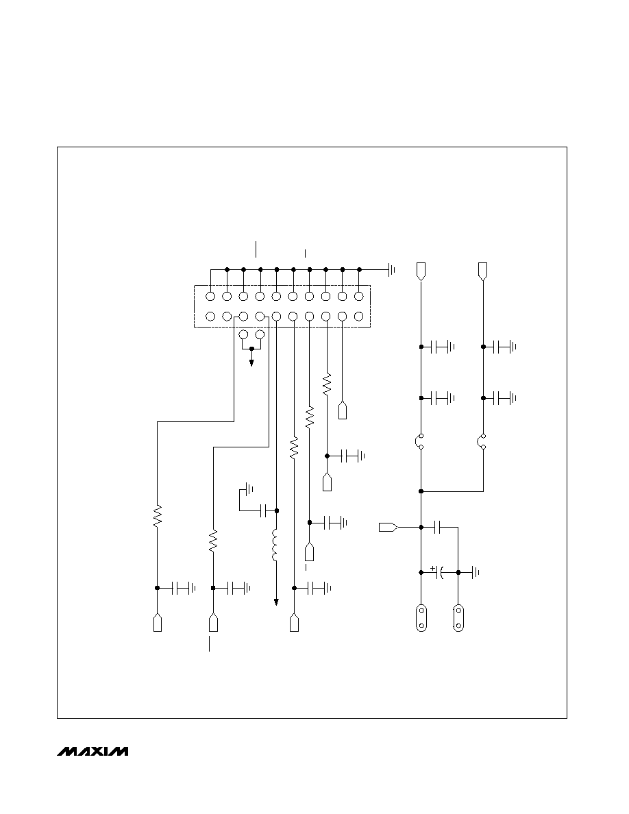
Evaluate: MAX2310/MAX2314
MAX2310/MAX2314 Evaluation Kits
_______________________________________________________________________________________
5
Figure 1. MAX2310EV Kit Schematic (continued)
R6
100
10
9
OPEN
OPEN
8
MODE
7
SHDN
6
FILTERED V
CC
5
DATA
4E
N
3
CLK
2
LOCK
1
C8
330pF
C12
330pF
C23
330pF
C24
330pF
C25
330pF
C37
0.01
µ
F
C27
10
µ
F
C28
0.01
µ
F
C38
0.01
µ
F
C33
47pF
C34
47pF
EN
CLK
R14
100
R16
100
R18
100
LOCK
C42
0.01
µ
F
L6
270nH
V
CC
DATA
SHDN
MODE
V
CC
A
V
CC
V
CC
V
CC
GND
V
CC
D
I
CC
D
I
CC
A
JU10
JU11
R8
100